EP1593955A2 - Wellenlängenabgestimmte Intensitätsmessung mit einem Oberflächenplasmonenresonanz-Sensor - Google Patents
Wellenlängenabgestimmte Intensitätsmessung mit einem Oberflächenplasmonenresonanz-Sensor Download PDFInfo
- Publication number
- EP1593955A2 EP1593955A2 EP05252740A EP05252740A EP1593955A2 EP 1593955 A2 EP1593955 A2 EP 1593955A2 EP 05252740 A EP05252740 A EP 05252740A EP 05252740 A EP05252740 A EP 05252740A EP 1593955 A2 EP1593955 A2 EP 1593955A2
- Authority
- EP
- European Patent Office
- Prior art keywords
- spr sensor
- wavelength
- optical system
- signal
- optical
- Prior art date
- Legal status (The legal status is an assumption and is not a legal conclusion. Google has not performed a legal analysis and makes no representation as to the accuracy of the status listed.)
- Withdrawn
Links
Images


Classifications
-
- G—PHYSICS
- G01—MEASURING; TESTING
- G01N—INVESTIGATING OR ANALYSING MATERIALS BY DETERMINING THEIR CHEMICAL OR PHYSICAL PROPERTIES
- G01N21/00—Investigating or analysing materials by the use of optical means, i.e. using sub-millimetre waves, infrared, visible or ultraviolet light
- G01N21/17—Systems in which incident light is modified in accordance with the properties of the material investigated
- G01N21/55—Specular reflectivity
- G01N21/552—Attenuated total reflection
- G01N21/553—Attenuated total reflection and using surface plasmons
Definitions
- the present invention relates in general to an optical system and to a related method, and in particular to an optical system comprising an SPR sensor.
- SPR Surface Plasmon Resonance
- the optical wavelength at which the dip occurs referred to as the resonant wavelength, is sensitive to changes in the refractive index of the dielectric that is adjacent to the conductive film. This sensitivity to changes in refractive index enables the dielectric to be used as a sensing medium, for example to detect and identify biological analytes, or for biophysical analysis of biomolecular interactions.
- measurement schemes that increase the accuracy with which changes in refractive index can be detected.
- measurement schemes that are scalable for use with analytical systems that include arrays of samples for biochemical sensing.
- an incident signal illuminates an SPR sensor over a wavelength range.
- Intensity of a reflected signal from the SPR sensor is detected with wavelength discrimination imposed on the incident signal or the reflected signal.
- the wavelength discrimination is imposed at a predesignated tuning rate within the wavelength range.
- the detected intensity is then sampled at a sampling rate and an intensity profile associated with the SPR sensor is established from the sampling with a wavelength resolution determined by the tuning rate and the sampling rate.
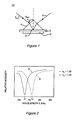
- Figure 1 shows an SPR sensor 10 that includes a conductive film 1 adjacent to a dielectric 2.
- the dielectric 2 is a sensing medium, and a linker layer (not shown) is interposed between the conductive film 1 and the dielectric 2 to provide a site for bio-molecular receptors to attach.
- the conductive film 1 in Figure 1 is shown adjacent to the dielectric 2 without the linker layer.
- a prism 4 is positioned adjacent to a side of the conductive film 1 that is opposite the dielectric 2.
- the conductive film 1 is a gold layer having an appropriate thickness for an incident optical signal, hereafter signal I INC , at a designated angle of incidence ⁇ INC and wavelength, to excite a surface plasmon wave, or surface plasmon, along the conductive film 1.
- signal I INC incident optical signal
- ⁇ INC angle of incidence
- ⁇ INC surface plasmon wave
- evanescent tail not shown
- Energy in the signal I INC that is not coupled into the surface plasmon is reflected at the conductive film 1 to provide a reflected optical signal, hereafter signal Ir.
- Coupling between the signal I INC and the surface plasmon results in a decrease, or dip, in the intensity of the signal Ir.
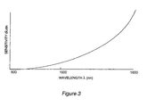
- the optical wavelength at which the dip occurs referred to as the resonant wavelength ⁇ R , is indicated in Figure 2 which shows exemplary intensity profiles. These intensity profiles show the relative intensity of the signal Ir versus the wavelength ⁇ of the signals I INC , Ir and indicate that the intensity of the signal Ir is sensitive to the wavelength ⁇ of the signals I INC , Ir in the vicinity of the resonant wavelength ⁇ R .
- the resonant wavelength ⁇ R is sensitive to changes ⁇ n in refractive index n S of the dielectric 2, due to the penetration of the evanescent tail into the dielectric 2.
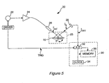
- Figure 3 shows that at longer optical wavelengths, the resonant wavelength ⁇ R has higher sensitivity to changes ⁇ n in the refractive index n S of the dielectric 2.
- the sensitivity of resonant wavelength ⁇ R to refractive index n S (indicated by the derivative d ⁇ /dn) correspondingly increases, which results in a larger shift ⁇ in resonant wavelength ⁇ R for each given change ⁇ n in refractive index n S .
- Figure 4 shows exemplary intensity profiles that indicate the relative intensity of the signal Ir versus the optical wavelength ⁇ of the signals I INC , Ir at designated angles of incidence of signals ⁇ INC of the signal I INC .
- larger shifts ⁇ in resonant wavelength ⁇ R result for a given change ⁇ n in refractive index n S .
- shifts ⁇ in resonant wavelength ⁇ R get progressively larger, from a shift ⁇ 1 to a shift ⁇ 3 , as wavelength ⁇ of the signals I INC , Ir increases.
- Figure 4 also indicates that while the sensitivity d ⁇ /dn increases at longer wavelength ⁇ , the dips in relative intensity become broader and less pronounced at the longer wavelengths, which makes it more difficult to accurately detect the resonant wavelength ⁇ R of the SPR sensor 10 using conventional techniques.
- Surface Plasmon Resonance Biosensors by Homola et al., in Optical Biosensors: Present and Future, edited by F. S. Ligler and C. A. Rowe Taitt, ISBN 0444509747, page 244, reports that narrow dips in intensity provide higher accuracy and resolution for SPR-based sensors.
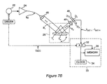
- Figure 5 shows an optical system 20 according to embodiments of the present invention.
- the optical system 20 is suitable for establishing intensity profiles associated with the SPR sensor 10, for detecting the resonant wavelength ⁇ R of an SPR sensor 10, or for detecting shifts ⁇ in resonant wavelength ⁇ R , such as shifts ⁇ induced by changes ⁇ n in refractive index n S of the dielectric 2 in an SPR sensor 10.
- shifts ⁇ in the resonant wavelength ⁇ R are detected and mapped to the changes ⁇ n in refractive index n S of the dielectric 2 that induce the shifts ⁇ .
- the optical system 20 includes a tunable optical source 22, typically a tunable laser such as an AGILENT TECHNOLOGIES, INC. model 81680B, that can be tuned at a tuning rate ⁇ within a wavelength range ⁇ 1 - ⁇ 2 .
- the wavelength range ⁇ 1 - ⁇ 2 in this example spans from at least 1492-1640 nanometers.
- Spectral bandwidth of the signal I INC provided by the tunable optical source 22 in the optical system is typically less than 100kHz, which is typically narrower than the shifts ⁇ in the resonant wavelength ⁇ R detected or measured by the optical system 20.
- the tunable optical source 22 is alternatively implemented with a tunable optical filter (not shown) cascaded with a white light or other broadband optical source (not shown) to provide a signal I INC that is spectrally narrow and tunable over the wavelength range ⁇ 1 - ⁇ 2 .
- tunable optical filters suitable for use in this type of tunable optical source 22 are available from MICRON OPTICS, Inc., Atlanta, GA., USA.
- An erbium-doped fiber amplifier (EDFA), or other type of optical amplifier 24, is optionally cascaded with the tunable optical source 22 to increase the power of the signal I INC that illuminates a region, or target T, of the SPR sensor 10.
- a collimator 26, or other beam-conditioning element, coupled to the tunable optical source 22 directs the signal I INC to the target T.
- the signal I INC includes a p-polarized lightwave and an s polarized lightwave that is orthogonal to the p polarized lightwave, where p, s refer to the conventionally defined polarizations p, s.
- the signal I INC can also be designated to be p polarized by including a polarization controller (not shown) in the signal path between the tunable optical source 22 and the collimator 26.
- a polarization controller (not shown) in the signal path between the tunable optical source 22 and the collimator 26.
- the signal I INC couples to the surface plasmon and causes the signal Ir to undergo the dip in intensity at the resonant wavelength ⁇ R , shown for example in the intensity profiles of Figure 2 and Figure 4.
- the optical system 20 is shown implemented using optical fiber in the optical path between the tunable optical source 22 and the collimator 26, free-space optics are alternatively used in this optical path to illuminate the target T of the SPR sensor 10.
- spatially separated quarter-wave plates and half-wave plates interposed between the tunable optical source 22 and the target T can be used to provide polarization adjustment to achieve a p polarized signal I INC .
- Polarization adjustment is alternatively provided via a polarization controller (not shown) interposed in the fiber optic signal path at the output of the tunable optical source 22.
- a detector 28 intercepts the signal I R as the wavelength ⁇ of the tunable optical source 22 is tuned within a wavelength range ⁇ 1 - ⁇ 2 that includes the resonant wavelength ⁇ R of the SPR sensor 10.
- the angle of incidence ⁇ INC can be adjusted so that at an adjusted angle of incidence, the resonant wavelength ⁇ R falls within the wavelength range ⁇ 1 - ⁇ 2 .
- Adjusting the angle of incidence ⁇ INC is typically enabled by mounting the SPR sensor 10 on a rotation stage 25.
- the detector 28 is typically a photodiode, photosensor or other transducer suitable for converting an intercepted optical signal into a corresponding electrical signal, hereinafter referred to as detected signal I DET .
- the detected signal I DET is provided to a processing unit 30 that in this example includes an analog to digital converter 32 that acquires samples of the detected signal I DET .
- This acquisition of the samples is triggered by a trigger signal TRIG provided by the tunable optical source 22, which indicates initiation of the tuning or sweeping of the tunable optical source 22.
- the rate of the sample acquisitions, or sample rate is determined by a clock rate f CLOCK established by a clock 34.
- the acquisitions result in a set S of samples of the detected signal I DET that is stored in a memory 36.
- Samples Si in the set S represent the detected intensity of the signal Ir at the wavelengths ⁇ i of the tunable optical source 22.
- Each integer sample number i corresponds to a wavelength ⁇ i within the wavelength range ⁇ 1 - ⁇ 2 .
- the detector 28 is typically a broadband detector, to accommodate the wavelength range ⁇ 1 - ⁇ 2 of the tunable optical source, the signal Ir intercepted by the detector is spectrally narrow at the wavelengths of the samples Si, so that wavelength resolution of the acquired samples Si in the set S is not compromised by the spectral width of the signal Ir.
- the wavelength ⁇ of the tunable optical source 22 being swept or tuned at the tuning rate ⁇ , the wavelength resolution with which the samples Si in the set S are acquired is based on the ratio of the clock rate f CLOCK and the tuning rate ⁇ .
- the intensity profile enables an accurate determination of the resonant wavelength ⁇ R of the SPR sensor 10, which can be used to accurately determine the resonant wavelength ⁇ R of the SPR sensor 10, or shifts ⁇ in the resonant wavelength ⁇ R , such as those shifts ⁇ induced by changes ⁇ n in the refractive index n S of the dielectric 2 of the SPR sensor 10.
- resonant wavelength ⁇ R can be determined from derivatives of the intensity profile to find the minimum of the intensity profile that corresponds to the resonant wavelength ⁇ R , or from any other suitable technique for identifying the resonant wavelength ⁇ R at the dip in the intensity profile.
- Shifts ⁇ in the resonant wavelength ⁇ R between two or more intensity profiles can be detected and quantified by determining the difference in resonant wavelengths ⁇ R of the two or more intensity profiles. Shifts in the intensity profile can also be associated with a change in one or more attributes of the SPR sensor such as a change in refractive index in a sensing medium of the SPR sensor 10.
- mapping between the shifts ⁇ and the changes ⁇ n is established from computer simulation of the SPR sensor 10 using MATLAB or other suitable program or environment that solves the Fresnel reflections at the interface between the conductive film 1 and the dielectric 2.
- the computer simulation models the sensitivity d ⁇ /dn S of the resonant wavelength ⁇ R to refractive index n S .
- each shift ⁇ in resonant wavelength ⁇ R can be mapped to a corresponding change ⁇ n in refractive index n S .
- multiple targets T having dielectrics 2 with different known refractive indices n S1 , n S2 ...n SX are illuminated sequentially or simultaneously by optical signals I INC1 , I INC2 ...I INC3 at wavelengths ⁇ in the vicinity of the resonant wavelength ⁇ R .
- resonant wavelengths ⁇ R1 , ⁇ R2 ... ⁇ RX corresponding to each of the refractive indices n S1 , n S2 ...n SX are determined. Curve-fitting of the resonant wavelengths ⁇ R1 , ⁇ R2 ... ⁇ RX to refractive indices n S1 , n S2 ...n SX , interpolation, or other suitable techniques are then used to establish a mapping between shifts ⁇ in resonant wavelength ⁇ R and changes ⁇ n in refractive index n S .
- the change ⁇ n in refractive index n S can be derived from the equation of the wave vectors k SPR , kx, as equation (1), where the imaginary component of the dielectric constant ⁇ 1 of the conductive film 1 is set to zero.
- ⁇ n ⁇ ( n 4 n 3 S ⁇ ( 1 ⁇ 1 -1)+ dn 4 d ⁇ n S (n 2 S + ⁇ 1 )) n 4 ⁇ 1
- mapping detected shifts in the resonant wavelength to changes ⁇ n in refractive index n S are exemplary. It is appreciated that any suitable scheme is alternatively used to establish this mapping.
- a white light or other spectrally broad optical source 42 within an optical system provides a signal IW INC that illuminates the SPR sensor 10.
- a signal IWr is reflected at the target T of the SPR sensor 10 and then filtered by a tunable optical filter 44 interposed between the SPR sensor 10 and the detector 28.
- the tunable optical filter 44 such as a diffraction grating or filters available from OMEGA OPTICAL, Inc., Brattleboro, VT., USA, has a spectrally narrow passband and is tunable within the wavelength range ⁇ 1 - ⁇ 2 .
- the detector 28 intercepts a resulting filtered signal I F from the tunable optical filter 44 as the passband of the tunable optical filter 44 is tuned within a wavelength range ⁇ 1 - ⁇ 2 that includes the resonant wavelength ⁇ R of the SPR sensor 10.
- the angle of incidence ⁇ INC of the signal IW INC can be adjusted via the rotational stage 25 so that at an adjusted angle of incidence, the resonant wavelength ⁇ R falls within the wavelength range ⁇ 1 - ⁇ 2 .
- the detector 28 produces the signal I DET .
- the detected signal I DET is then provided to the processing unit 30, which acquires the set S of samples.
- the set S of samples is processed to establish an intensity profile associated with the SPR sensor 10 to detect the resonant wavelength ⁇ R of the SPR sensor 10, or to detect shifts ⁇ in the resonant wavelength ⁇ R of the SPR sensor 10 resulting from changes ⁇ n in refractive index n S .
- the shifts ⁇ in the resonant wavelength ⁇ R can then be mapped to changes ⁇ n in refractive index n S .
- FIGS 7A-7B Alternative embodiments of the present invention, shown in Figures 7A-7B, enable simultaneous or sequential detection of induced shifts ⁇ in resonant wavelength ⁇ R from an array of targets T 1 -T N included in one or more SPR sensors 10.
- the targets T 1 -T N are illuminated by optical signals I INC1 -I INCN provided from an optical signal I INC by an optical splitter 46 and directed via collimators 26 1 -26 N .
- An imaging element such as a lens (not shown) is optionally interposed between the array of targets T 1 -T N and an array of detector elements D 1 -D N in the detector 28, such as a photodiode array.
- the imaging element provides a mapping or other correspondence between the physical locations of the targets T 1 -T N and physical locations of detector elements D 1 -D N in the detector array, so that optical signals Ir 1 -Ir N reflected from the array of targets T 1 -T N are intercepted by corresponding detector elements D 1 -D N in the detector array to provide detected signals I DET1 -I DETN .
- the beams of the optical signals Ir 1 -Ir N reflected from the array of targets T 1 -T N are spatially distinct, a correspondence between the array of targets T 1 -T N and the array of detector elements D 1 -D N is provided via the optical signals Ir 1 -Ir N .
- a physical mapping or other correspondence between the array of targets T 1 -T N and the array of detector elements D 1 -D N can be provided by interposing the imaging element between the array of targets T 1 -T N and the array of detector elements D 1 -D N .
- the detected signals I DET1 -I DETN from the array of detector elements D 1 -D N are then provided to the processing unit 30, which acquires sets S 1 -S N of samples that correspond to each of the targets T 1 -T N .
- the sets S 1 -S N of samples are processed to determine the resonant wavelengths ⁇ R , or shifts ⁇ in the resonant wavelengths ⁇ R of the targets T 1 -T N resulting from changes in refractive indices of the targets T 1 -T N .
- the shifts ⁇ in the resonant wavelength ⁇ R can then be mapped to changes ⁇ n in refractive index n S .
- a collimating element 48 such as a lens forms a beam B1 from the optical signal I INC that is suitably wide to illuminate an array of targets T 1 -T N .
- spatially separated quarter-wave plates and half-wave plates can be interposed between the tunable optical source and the array of targets T 1 -T N to provide polarization adjustment to achieve a p polarization of the beam B1.
- Polarization adjustment is alternatively provided via a polarization controller (not shown) interposed in the fiber optic signal path at the output of the tunable optical source 22.
- a beam B2 is reflected.
- An imaging element 49 positioned in the optical path between the array of targets T 1 -T N and the detector 28, provides a correspondence between the physical locations of the targets T 1 -T N and physical locations of detector elements D 1 -D N in the detector 28, so that portions of the beam B2 reflected from the corresponding targets positioned within the array of targets T 1 -T N are intercepted by corresponding detector elements D 1 -D N in the detector 28 to provide detected signals I DETI -I DETN .
- the sets S 1 -S N of samples are processed to determine the resonant wavelengths ⁇ R , or shifts ⁇ in the resonant wavelengths ⁇ R of the targets T 1 -T N resulting from changes ⁇ n 1 - ⁇ n N in refractive indices of the targets T 1 -T N .
- the shifts ⁇ in the resonant wavelength ⁇ R can then be mapped to changes ⁇ n in refractive index n S .
- shifts ⁇ in resonant wavelength ⁇ R have been mapped to changes ⁇ n in refractive index n S of the dielectric 2. These changes ⁇ n in refractive index n S can then be used to detect and identify biological analytes, or for biophysical analysis of biomolecular interactions.
- the shifts ⁇ in the resonant wavelength ⁇ R are mapped to the presence or identity of biological analytes, to biophysical analyses of biomolecular interactions, or to any suitable attributes or features of the SPR sensor 10 that induce the shifts ⁇ in the resonant wavelength ⁇ R .
- the resonant wavelength associated with the SPR sensor 10 is typically the wavelength at which the dip in the intensity profile occurs, as shown for example in Figures 2 and 4.
- the resonant wavelength ⁇ R associated with the SPR sensor 10 is alternatively any other designated measurement wavelength, such as one or more wavelengths ⁇ offset from the actual resonant wavelength at which the dip in the intensity profile occurs.
- These measurement wavelengths can be used to detect shifts ⁇ in the resonant wavelength ⁇ R , such as those shifts ⁇ due to changes in the refractive index n S of the dielectric 2.
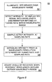
- FIG 8 shows a measurement method 50 according to alternative embodiments of the present invention.
- the measurement method 50 includes illuminating the SPR sensor 10 over the wavelength range ⁇ 1 - ⁇ 2 with an incident optical signal, such as the signals I INC , IW INC (step 52).
- the intensity of the reflected signal from the SPR sensor is detected with wavelength discrimination imposed, at a pre-established tuning rate within the wavelength range ⁇ 1 - ⁇ 2 , on the incident signal or the reflected signal.
- Wavelength discrimination is imposed on the incident signal I INC by generating the incident signal with the tunable optical source 22.
- wavelength discrimination is imposed on the incident signal I INC via a tunable optical filter interposed between an optical source generating the incident signal and the SPR sensor 10.
- Wavelength discrimination is imposed on the reflected signal via the tunable optical filter 44 interposed between the SPR sensor 10 and the detector 28 detecting the intensity of the reflected signal from the SPR sensor 10.
- Step 56 of the measurement method 50 includes sampling the detected intensity at a sampling rate.
- Step 58 includes establishing an intensity profile associated with the SPR sensor from the sampling of step 56, where the intensity profile has a wavelength resolution determined by the tuning rate ⁇ and the sampling rate.
- the measurement method 60 optionally comprises step 59, which includes adjusting the angle of incidence of the incident signal on the SPR sensor 10 when an identified resonant wavelength ⁇ R associated with the SPR sensor 10 occurs outside the wavelength range ⁇ 1 - ⁇ 2 , so that at an adjusted angle of incidence, the resonant wavelength ⁇ R of the SPR sensor 10 falls within the designated wavelength range ⁇ 1 - ⁇ 2 .
- SPR sensors in these embodiments are meant to include resonant mirror transducers, or any other type of transducer providing reflected optical signals Ir having associated intensity profiles dependent on attributes of a sensing medium that are sensed by penetration of an evanescent wave into the sensing medium.
Applications Claiming Priority (2)
| Application Number | Priority Date | Filing Date | Title |
|---|---|---|---|
| US10/838,790 US20050244093A1 (en) | 2004-05-03 | 2004-05-03 | Wavelength-tuned intensity measurement of surface plasmon resonance sensor |
| US838790 | 2004-05-03 |
Publications (2)
| Publication Number | Publication Date |
|---|---|
| EP1593955A2 true EP1593955A2 (de) | 2005-11-09 |
| EP1593955A3 EP1593955A3 (de) | 2006-05-17 |
Family
ID=34941138
Family Applications (1)
| Application Number | Title | Priority Date | Filing Date |
|---|---|---|---|
| EP05252740A Withdrawn EP1593955A3 (de) | 2004-05-03 | 2005-05-03 | Wellenlängenabgestimmte Intensitätsmessung mit einem Oberflächenplasmonenresonanz-Sensor |
Country Status (3)
| Country | Link |
|---|---|
| US (1) | US20050244093A1 (de) |
| EP (1) | EP1593955A3 (de) |
| JP (1) | JP2005321385A (de) |
Cited By (2)
| Publication number | Priority date | Publication date | Assignee | Title |
|---|---|---|---|---|
| WO2009082353A1 (en) * | 2007-12-20 | 2009-07-02 | Knut Johansen | Spr apparatus and method |
| CN105699335A (zh) * | 2016-04-12 | 2016-06-22 | 岭南师范学院 | 一种多功能spr检测仪 |
Families Citing this family (7)
| Publication number | Priority date | Publication date | Assignee | Title |
|---|---|---|---|---|
| US7473916B2 (en) * | 2005-12-16 | 2009-01-06 | Asml Netherlands B.V. | Apparatus and method for detecting contamination within a lithographic apparatus |
| JP4898263B2 (ja) * | 2006-04-07 | 2012-03-14 | サンテック株式会社 | 光干渉断層画像表示システム |
| EP2335050A4 (de) * | 2008-09-30 | 2014-01-15 | Univ Montreal | Hochauflösendes oberflächenplasmonen-resonanzinstrument mit einem dove-prisma |
| US8384905B2 (en) * | 2009-11-10 | 2013-02-26 | Corning Incorporated | Tunable light source for label-independent optical reader |
| ES2363955B1 (es) * | 2010-02-09 | 2012-09-04 | Consejo Superior de Invetigaciones Cientificas | Metodo para el analisis del indice de refraccion de un medio dielectrico adyacente a un medio plasmonico, y dispositivo correspondiente |
| CN111368480B (zh) * | 2020-03-11 | 2023-12-22 | 深圳大学 | Spr传感器灵敏度检测分析的方法及系统 |
| CN113466178A (zh) * | 2021-06-30 | 2021-10-01 | 南京品傲光电科技有限公司 | 一种基于spw的在线型微腔光纤传感器及其制作方法 |
Citations (5)
| Publication number | Priority date | Publication date | Assignee | Title |
|---|---|---|---|---|
| WO1996002823A1 (en) * | 1994-07-20 | 1996-02-01 | Scientific Generics Limited | Surface plasmon resonance sensors and methods of operation |
| WO1999030135A1 (en) * | 1997-12-12 | 1999-06-17 | The Perkin-Elmer Corporation | Optical resonance analysis system |
| US5999262A (en) * | 1996-04-19 | 1999-12-07 | Carl Zeiss Jena Gmbh | Process and apparatus for detecting structural changes of specimens |
| US6542241B1 (en) * | 1999-03-25 | 2003-04-01 | Jena-Optronik Gmbh | Arrangement for optically reading out the information from substrates having a multiplicity of individual samples |
| US20030081875A1 (en) * | 2001-10-26 | 2003-05-01 | Vladimir Kochergin | System and method for measuring physical, chemical and biological stimuli using vertical cavity surface emitting lasers with integrated tuner |
-
2004
- 2004-05-03 US US10/838,790 patent/US20050244093A1/en not_active Abandoned
-
2005
- 2005-04-15 JP JP2005118388A patent/JP2005321385A/ja active Pending
- 2005-05-03 EP EP05252740A patent/EP1593955A3/de not_active Withdrawn
Patent Citations (5)
| Publication number | Priority date | Publication date | Assignee | Title |
|---|---|---|---|---|
| WO1996002823A1 (en) * | 1994-07-20 | 1996-02-01 | Scientific Generics Limited | Surface plasmon resonance sensors and methods of operation |
| US5999262A (en) * | 1996-04-19 | 1999-12-07 | Carl Zeiss Jena Gmbh | Process and apparatus for detecting structural changes of specimens |
| WO1999030135A1 (en) * | 1997-12-12 | 1999-06-17 | The Perkin-Elmer Corporation | Optical resonance analysis system |
| US6542241B1 (en) * | 1999-03-25 | 2003-04-01 | Jena-Optronik Gmbh | Arrangement for optically reading out the information from substrates having a multiplicity of individual samples |
| US20030081875A1 (en) * | 2001-10-26 | 2003-05-01 | Vladimir Kochergin | System and method for measuring physical, chemical and biological stimuli using vertical cavity surface emitting lasers with integrated tuner |
Non-Patent Citations (5)
| Title |
|---|
| HOMOLA J ET AL: "Surface plasmon resonance sensors based on diffraction gratings and prism couplers: sensitivity comparison" SENSORS AND ACTUATORS B, ELSEVIER SEQUOIA S.A., LAUSANNE, CH, vol. 54, no. 1-2, 25 January 1999 (1999-01-25), pages 16-24, XP004163208 ISSN: 0925-4005 * |
| HOMOLA J ET AL: "Surface plasmon resonance sensors: review" SENSORS AND ACTUATORS B, ELSEVIER SEQUOIA S.A., LAUSANNE, CH, vol. 54, no. 1-2, 25 January 1999 (1999-01-25), pages 3-15, XP004163207 ISSN: 0925-4005 * |
| HOMOLA JIRÍ: "Present and future of surface plasmon resonance biosensors." ANALYTICAL AND BIOANALYTICAL CHEMISTRY. OCT 2003, vol. 377, no. 3, October 2003 (2003-10), pages 528-539, XP002372993 ISSN: 1618-2642 * |
| WU C-M ET AL: "High-sensitivity sensor based on surface plasmon resonance and heterodyne interferometry" SENSORS AND ACTUATORS B, ELSEVIER SEQUOIA S.A., LAUSANNE, CH, vol. 92, no. 1-2, 1 July 2003 (2003-07-01), pages 133-136, XP004424468 ISSN: 0925-4005 * |
| YEATMAN E M: "Resolution and sensitivity in surface plasmon microscopy and sensing" BIOSENSORS & BIOELECTRONICS ELSEVIER UK, vol. 11, no. 6-7, 1996, pages 635-649, XP002372994 ISSN: 0956-5663 * |
Cited By (4)
| Publication number | Priority date | Publication date | Assignee | Title |
|---|---|---|---|---|
| WO2009082353A1 (en) * | 2007-12-20 | 2009-07-02 | Knut Johansen | Spr apparatus and method |
| US8462344B2 (en) | 2007-12-20 | 2013-06-11 | Knut Johansen | SPR apparatus and method |
| CN105699335A (zh) * | 2016-04-12 | 2016-06-22 | 岭南师范学院 | 一种多功能spr检测仪 |
| CN105699335B (zh) * | 2016-04-12 | 2019-01-04 | 岭南师范学院 | 一种多功能spr检测仪 |
Also Published As
| Publication number | Publication date |
|---|---|
| US20050244093A1 (en) | 2005-11-03 |
| JP2005321385A (ja) | 2005-11-17 |
| EP1593955A3 (de) | 2006-05-17 |
Similar Documents
| Publication | Publication Date | Title |
|---|---|---|
| EP1574832A2 (de) | Messung der optischen Phase eines Ziels | |
| US5255075A (en) | Optical sensor | |
| EP1593955A2 (de) | Wellenlängenabgestimmte Intensitätsmessung mit einem Oberflächenplasmonenresonanz-Sensor | |
| JP3076604B2 (ja) | 表面プラズモン共鳴装置 | |
| US10365163B2 (en) | Optical critical dimension metrology | |
| US5991048A (en) | Surface plasmon resonance light pipe sensor | |
| US5581350A (en) | Method and system for calibrating an ellipsometer | |
| US4999014A (en) | Method and apparatus for measuring thickness of thin films | |
| KR100484377B1 (ko) | 분광 엘립소미터 | |
| CN101371129B (zh) | 表面等离子体共振传感器以及利用其检测样品的方法 | |
| US7619725B1 (en) | Optically amplified critical wavelength refractometer | |
| US7889339B1 (en) | Complementary waveplate rotating compensator ellipsometer | |
| US7812955B2 (en) | Sample analysis apparatus and analysis method | |
| US6885454B2 (en) | Measuring apparatus | |
| CN110927121B (zh) | 一种基于白光干涉光谱的相位型spr检测装置及方法 | |
| JP2004509351A (ja) | 光学信号の波長を検出する波長検出器及び方法 | |
| CN110927122B (zh) | 一种基于干涉光谱的相位型spr检测装置及方法 | |
| KR101987402B1 (ko) | 편광픽셀어레이를 이용한 박막과 후막의 두께 및 삼차원 표면 형상 측정 광학 장치 | |
| WO2004064969A1 (en) | Crystal grating apparatus | |
| EP1394532A2 (de) | Messvorrichtung | |
| US6654123B2 (en) | Sensor utilizing attenuated total reflection | |
| US20070216901A1 (en) | Ellipsometry Device Provided With A Resonance Platform | |
| GB2268800A (en) | Optical sensor | |
| JP2004085487A (ja) | 全反射減衰を利用したセンサー | |
| JP2003227792A (ja) | 全反射減衰を利用したセンサー |
Legal Events
| Date | Code | Title | Description |
|---|---|---|---|
| PUAI | Public reference made under article 153(3) epc to a published international application that has entered the european phase |
Free format text: ORIGINAL CODE: 0009012 |
|
| AK | Designated contracting states |
Kind code of ref document: A2 Designated state(s): AT BE BG CH CY CZ DE DK EE ES FI FR GB GR HU IE IS IT LI LT LU MC NL PL PT RO SE SI SK TR |
|
| AX | Request for extension of the european patent |
Extension state: AL BA HR LV MK YU |
|
| PUAL | Search report despatched |
Free format text: ORIGINAL CODE: 0009013 |
|
| AK | Designated contracting states |
Kind code of ref document: A3 Designated state(s): AT BE BG CH CY CZ DE DK EE ES FI FR GB GR HU IE IS IT LI LT LU MC NL PL PT RO SE SI SK TR |
|
| AX | Request for extension of the european patent |
Extension state: AL BA HR LV MK YU |
|
| AKX | Designation fees paid | ||
| RAP1 | Party data changed (applicant data changed or rights of an application transferred) |
Owner name: AGILENT TECHNOLOGIES, INC. |
|
| REG | Reference to a national code |
Ref country code: DE Ref legal event code: 8566 |
|
| STAA | Information on the status of an ep patent application or granted ep patent |
Free format text: STATUS: THE APPLICATION IS DEEMED TO BE WITHDRAWN |
|
| 18D | Application deemed to be withdrawn |
Effective date: 20061201 |