EP1590727B1 - Asynchrone hüllschaltung für eine global asynchrone, lokal synchrone (gals) schaltung - Google Patents
Asynchrone hüllschaltung für eine global asynchrone, lokal synchrone (gals) schaltung Download PDFInfo
- Publication number
- EP1590727B1 EP1590727B1 EP03785953A EP03785953A EP1590727B1 EP 1590727 B1 EP1590727 B1 EP 1590727B1 EP 03785953 A EP03785953 A EP 03785953A EP 03785953 A EP03785953 A EP 03785953A EP 1590727 B1 EP1590727 B1 EP 1590727B1
- Authority
- EP
- European Patent Office
- Prior art keywords
- signal
- asynchronous
- timing
- unit
- clock
- Prior art date
- Legal status (The legal status is an assumption and is not a legal conclusion. Google has not performed a legal analysis and makes no representation as to the accuracy of the status listed.)
- Expired - Lifetime
Links
Images



Classifications
-
- G—PHYSICS
- G06—COMPUTING OR CALCULATING; COUNTING
- G06F—ELECTRIC DIGITAL DATA PROCESSING
- G06F1/00—Details not covered by groups G06F3/00 - G06F13/00 and G06F21/00
- G06F1/04—Generating or distributing clock signals or signals derived directly therefrom
- G06F1/08—Clock generators with changeable or programmable clock frequency
-
- G—PHYSICS
- G06—COMPUTING OR CALCULATING; COUNTING
- G06F—ELECTRIC DIGITAL DATA PROCESSING
- G06F1/00—Details not covered by groups G06F3/00 - G06F13/00 and G06F21/00
- G06F1/04—Generating or distributing clock signals or signals derived directly therefrom
- G06F1/12—Synchronisation of different clock signals provided by a plurality of clock generators
Definitions
- the invention relates to an asynchronous envelope circuit for a globally asynchronous, locally synchronous (GALS) circuit. It further relates to a GALS circuit and a method of clocking an internally synchronous circuit block.
- GALS globally asynchronous, locally synchronous
- a data path architecture system typically includes complex circuit blocks that perform expensive arithmetic or trigonometric operations.
- FFT / IFFT fast Fourier transform / invertide FFT
- An essential technical problem of modern ASICs is the synchronization of the different function blocks integrated on a chip.
- the use of a global time clock for all function blocks can be realized in the design only with great effort.
- a synchronous, global clock generates increased electromagnetic interference (EMI). This complicates the integration of analog and digital circuits on a chip.
- EMI electromagnetic interference
- GALS global asynchronous locally synchronous
- Asynchronous circuits dispense with a time frame with discrete time steps.
- the function of asynchronous circuits is based on the occurrence of events.
- the current state of the circuit is completely determined by the polarity of signal changes and their order.
- GALS circuits have circuit blocks which operate internally synchronously. These locally synchronous circuit blocks communicate with each other in asynchronous, that is, using a handshake protocol. Therefore, there is no need to synchronize the individual locally synchronized circuit blocks with each other globally. As long as each individual locally synchronous block follows the handshake protocol, these circuit blocks can be combined with each other in any manner.
- a GALS architecture is characterized by a modular structure that allows high flexibility of the circuit design. Because the interface to each locally synchronous circuit module is asynchronous, any synchronous circuits can be integrated with each other. Each locally synchronous circuit block may have a time frame with individual clock signal frequency.
- asynchronous wrapper To implement the asynchronous communication between the locally synchronous circuit blocks, these each have an asynchronous wrapper, which is also referred to as an "asynchronous wrapper".
- An asynchronous wrapper has input and output ports and a local clock signal generator.
- Each port of the wrapper that is, each input and each output has an associated port controller responsible for implementing the handshake protocol. Port and control together form an input or output unit.
- the clock signal generator of an asynchronous envelope circuit is designed to generate the clock signal with a tunable in a certain frequency range signal frequency.
- An important feature of asynchronous envelope clock signal generators is that the generation of the clock signal is pausable.
- Tormod Njolstad et al. "A Socket Interface for GALS Using Locally Dynamic Voltage Scaling for Rate-Adaptive Energy Saving," IEEE, September 2001, provides an envelope circuit that adjusts the local clock to the required data processing rate and exposes the local clock a "timer" known.
- circuit blocks can be clocked individually internally synchronously and at the same time exchange data asynchronously with circuit blocks of the environment.
- this asynchronous wrapper is designed for unspecified applications and therefore is not adapted to given in individual cases circuit environments. This applies in particular with regard to the power consumption required for a GALS block. Mechanisms for reducing the power consumption are difficult to realize with the known asynchronous envelopes.
- the technical problem underlying the present invention is to provide an asynchronous wrapper that allows the realization of a GALS block with low power consumption.
- an asynchronous wrapper is provided with at least one input unit configured to externally receive a request signal and to externally indicate receipt of the request signal by issuing an associated acknowledge signal, a suspendable clock unit is configured to repeatedly generate a first clock signal and deliver it to an internally synchronous circuit block associated with the asynchronous envelope circuit, wherein the input unit is formed in that, upon receipt of a request signal, generate and deliver to the internally synchronous circuit block a timed signal associated with the request signal, and wherein a timeout unit connected to the input unit is provided and adapted to deliver the first one Suppress clock signal.
- the invention is based on the recognition that a GALS block for processing a continuous data stream operates most effectively in quasi-synchronous operation.
- a quasi-synchronous operation can be realized according to the invention, in which a GALS block is operated in a request-driven operating module.
- the internally synchronous circuit block is thus always clocked when data actually arrive at its input.
- Request signals are received externally, i.e., from an adjacent asynchronous wrapper preceding in the data flow in an asynchronous wrapper, when data is present for input to the local, internally synchronous circuit block.
- the device according to the invention can also operate without exposable clock unit and without time-out unit. This has the consequence that it is clocked alone with the help of the second clock signals. In the absence of request signals, the locally synchronous circuit would not be clocked in this case. Although this has the disadvantage that remaining in the pipeline of the synchronous circuit data are not output. But with a renewed arrival of request signals, the output would continue.
- the internally synchronous circuit is clocked to avoid this disadvantage according to claim 1 by means of two alternative sources, either by means of the clock unit, or by means of the input unit due to request signals.
- the synchronized with incoming request signals Clocking by the "second" clock signals has priority over clocking with the aid of "first" clock signals from the clock unit. However, it is ensured that one clock period of a "first" clock signal is terminated before a "second” clock signal is delivered to the internally synchronous circuit block.
- a second clock signal is synchronized with a currently received request signal by generating the second clock signal in a defined temporal relationship to the request signal.
- the defined temporal relationship may mean, for example, that rising edge and falling edge of the second clock signal are generated at a fixed time interval to the rising edge and falling edge of the request signal.
- the arrangement according to the invention has various advantages. It initially allows for a renunciation of a global clock tree. If there are no request signals from the outside, the arrangement according to the invention allows a clocking with the aid of the first clock signals only when needed, that is, for example, as long as there are data for delivery to the outside in the pipeline of internally synchronous circuit.
- the asynchronous wrapper according to the invention therefore enables a low power consumption of a GALS block oriented on the actual data processing requirement.
- due to the dependent of request signals timing only a few boundary conditions for the clock frequency of the local clock generator, which generates the "first" clock signals.
- the clock frequency of a local clock generator does not have to be adapted to the data rate. This allows a simple design of the ring oscillator of the local clock generator.
- the timeout unit is designed to emit a control signal for enabling the delivery of the first clock signal when a predetermined period of time has elapsed after the last second clock signal has been output.
- a so-called time-out period is awaited after the last request signal, before the timing by the local clock generator replaces the timing with incoming request signals.
- this has the advantage that the clock does not unintentionally jump back and forth between the first and second clock signal if only a request signal is not present for a short time.
- the release of the first clock signal it is possible, independently of the presence of a request signal, to empty the pipeline of the local, internally synchronous circuit and thus to obtain a coherent data flow over several GALS blocks as such.
- a second embodiment which is alternative to the first embodiment, is based on the idea of providing a supplement to the communication protocol between the asynchronous envelopes of adjacent GALS blocks instead of waiting for a certain period of time with the aid of the time-out unit.
- the asynchronous wrapper of the previous GALS block indicates that a current request signal is the last request signal for the time being.
- the signal may be a modified request signal or a separate signal to be sent in parallel with a request signal.
- the output unit of the asynchronous envelope circuit can be formed.
- the corresponding circuit implementation is known per se to the person skilled in the art.
- the input unit is designed to receive the signal. It may also perceive the function of outputting the enable signal for the first clock signal performed by the TimP-Out unit in the first embodiment.
- clocking with the aid of the first clock signal should only take place in the first and second embodiments take place as data is present in the pipeline.
- a clock control unit coupled to the clock unit and to the input unit and configured to drive the clock unit to output a number of clock pulses, the number of clock pulses being less than or equal to the depth of a pipeline of the associated internally synchronous circuit block.
- the clock control unit is preferably designed to send the clock unit a control signal for stopping after the said number of clock pulses has been output.
- the input unit is preferably designed to output a control signal to the internally synchronous circuit block for activating a data input when a request signal is present.
- Several input units can be provided. This is useful, for example, if the GALS block is connected on the input side to several other GALS blocks.
- one or more output units may be provided, which are configured to send a request signal to the outside and to emit a control signal to the internally synchronous circuit block for enabling a data output upon receiving an acknowledgment signal from the outside.
- communication takes place between an output unit of a first GALS block on the one hand and a connected input unit of a second GALS block via a four-phase handshake protocol known per se to the person skilled in the art.
- the input unit and the output unit are preferably each designed to communicate with the aid of the four-phase handshake protocol.
- GALS blocks can be realized with an internally synchronous circuit block and an asynchronous wrapper. From various such GALS blocks can be realized in highly integrated circuits GALS architectures comprising at least one internally synchronous circuit block and each associated asynchronous envelope.
- a data latch of the internally synchronous circuit block is preceded by a data latch whose operation is controlled by the input unit.
- a data latch whose operation is controlled by the input unit.
- the data latch prevents the occurrence of metastable states at the input of the internally synchronous circuit block.
- the method according to the invention breaks with the asynchronous clock method common in connection with GALS architectures, in which the local clock signal can be delayed as required. Instead, it proposes a timing oriented to the presence of a request signal.
- the local (first) clock signal is suspended or the local clock signal generator is turned off.
- a clock signal referred to as the "second clock signal" in the context of the present application, is directly derived for the locally synchronous block.
- the local clock generator is used exclusively to empty internal pipeline stages of the locally synchronous circuit when no external request signal is present for a certain period of time.
- An exemplary embodiment of the method according to the invention includes a switchover to the output of the first clock signal generated with the aid of the local clock signal generator in the absence of a request signal over a predeterminable period of time.
- the local clock signal generator is preferably switched off again after emptying a pipeline of the internally synchronous circuit block or after the arrival of a new request signal.
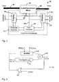
- FIG. 1 shows a simplified block diagram of a circuit 10 having a locally synchronous block 12 and an asynchronous wrapper 14.
- the locally synchronous block 12 has inputs and unspecified here Outputs for data exchanged with adjacent circuit blocks. This is symbolized by arrows 16 and 18.
- the asynchronous wrapper of the circuit 10 has an input 20 for receiving and transmitting handshake signals.
- the input communicates with the aid of the handshake signals, for example, with an output of a preceding in the data flow, adjacent, similar asynchronous wrapper, which is not shown.
- Connected to the input 20 is an output 22 which exchanges handshake signals in an analogous manner with the environment.
- the output 22 communicates with an input of an adjacent, similar, asynchronous wrapper, which is also not shown in the data flow.
- a time-out detector 24 is connected on the one hand to the input 20 and on the other hand to a clock signal generator 26. The connection of the clock signal generator 26 with the time-out detector 24 via control inputs. Similarly, the clock signal generator 26 is connected to the output 22 via control inputs and outputs.
- the local synchronous block 12 is a clock signal of the clock signal generator 26th or request signals of external circuits supplied from the input 20 ago.
- the locally synchronous circuit 12 is thus driven by both incoming request signals from external circuits and the local clock signal.
- a request signal which is passed through the input 20, comes from an asynchronous wrapper of an adjacent circuit block. It is synchronized with data reaching the locally synchronous block 12 via the data line 16.
- Each locally synchronous block 12 of different circuits 10 combined in one system has its own asynchronous wrapper.
- This asynchronous wrapper additionally sends signals to neighboring wrappers that provide information about the current state of the wrapper.
- a token is the combination of a data unit with information on the validity of this data unit.
- the adjacent envelopes operate their respective locally synchronous block 12 in response to this signal.
- the modules belonging to a locally synchronous block generate another signal for transmission to the functionally succeeding module indicating the end of operation. Depending on this signal, the module accepts the data from the previous module and processes it.
- the envelope circuit 14 changes to another state in which it generates internal clock signals with the aid of a local ring oscillator described in more detail below.
- the number of internally generated clock signals is set equal to the number of clock cycles needed to empty the pipeline of the locally synchronous circuit 12. As soon as valid data is no longer in the synchronous block, the clock signal generator 26 stops. The locally synchronous block 12 is then inactive until a next request signal arrives.
- the arrival of a request signal is detected at a change of state at the input 20.
- the detection of a rising signal edge is interpreted as the arrival of a new request signal.
- the current clock cycle must first be terminated to prevent metastability at the data inputs of the locally synchronous block 12. Subsequently, the clock signal generation can be transferred from the local ring oscillator of the clock signal generator 26 to the input line 30. To avoid metastability in the handling of this situation, further circuits are required, which are described in more detail below.
- the circuit architecture proposed here has numerous advantages. As in any GALS system, no global clock tree is required initially.
- the clock signal is generated by "multiplexing" the local clock signal and the request signals. Due to the operation driven by request signals, the frequency of the local clock signal generator need not precisely match the frequency of a global clock signal generator or the data rate. This reduces the number of constraints on the design of the ring oscillator:
- the present implementation also does not require large input data register capacity in the locally synchronous block 12. This avoids unwanted delay while simplifying the hardware structure of the system.
- the locally synchronous block 12 responds directly to request signals in the concept provided here, thus avoiding delays.
- Another advantage of using a data flow approach in the circuit design proposed herein is that instead of locally synchronous pipelines, asynchronous circuits can be used as completely as desired.
- a respective synchronous block 12 is always driven only when data is present at its input or when it is necessary to drive out the data still remaining in the local pipeline. At all other times, the locally synchronous block 12 is out of service.
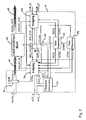
- FIG. 2 shows a detailed block diagram of the GALS block of FIG. 1.
- the asynchronous wrapper 14 has a clock controller 32 and a transparent latch 34 in addition to the elements shown in FIG.
- the function of the asynchronous envelope circuit 14 will be explained in more detail below with reference to FIGS. 2 to 9.
- the connecting lines indicate the transmission direction of the signals by the direction of the arrow.
- the clocking of the locally synchronous module 12 takes place with a signal IN T CLK.
- the signal INT_CLK is the output signal of an OR gate 36 at the inputs of which a signal REQ_INT and on the other hand a signal LCLKM is present.
- the signal REQ_INT is generated by the input 20, when a request signal REQ_A over the time-out generator 24 in the form of another signal has been received at the input REQ_A1 externally. Details of the structure and function of the time-out generator 24 are explained below in connection with FIG.
- the signal LCLKM is the output signal of an AND gate 38, whose two inputs are connected to the one with the clock generator 26 and the other with the time-out generator 24.
- the function of the AND gate 38 is to allow the time-out generator 24 by a signal ST, a control of the transfer of the output signal LCLK of the clock generator 26 to the OR gate 36.
- External data signals DATA_IN are buffered in the transparent latch 34 via the data line 16. This is required to get one metastable state at the input of the locally synchronous block to avoid.
- the operation of the latch 34 is controlled by a signal DLE, the register being transparent when the signal DLE is present.
- the signal DLE is present after a signal change of the clock generator 26 when previously stored in the latch data has already been written to the register stage of the locally synchronous module 12. It is not necessary for the locally synchronous module 12 to have further registers.
- the incoming data may be fed directly to a logic block (not shown) preceding the first register stage (also not shown).
- suspendable clock generator 26 The structure and the function of the suspendable clock generator 26 will be explained in more detail below with reference to FIG.
- the local clock signal generator 26 has a ring oscillator 39 comprising a Muller-C element 40, a delay line 44 and an OR gate (with downstream inverter) 46.
- the ring oscillator 29 receives signals, on the one hand from an arbiter 42 and the other via a second input of the OR gate 46.
- the OR gate 46 To the OR gate 46, on the one hand, the output signal LCLK of the ring oscillator is returned.
- the OR gate 46 is connected to an output of the clock controller 32, via which a signal STOPI can be applied.
- the STOPI signal is present in two cases: on the one hand immediately after a reset, in order to prevent the activation of the oscillator before the arrival of the first request signal at the local block. On the other hand, after a time-out, that is, when the number of local clock cycles equals the number of cycles necessary to output all valid data within the pipeline. In this situation, the local clock signal is blocked to prevent unnecessary power consumption.
- the ring oscillator 39 can assume three basic modes: sleep mode, time-out measurement mode and clock-merger mode.
- sleep mode a blocked Stop signal STOPI operation of the clock generator 26.
- time-out measuring mode the input handshake is enabled and the input waits for the occurrence of a time-out event.
- a time-out event is the absence of a request signal at the input for a predetermined time (T time-out ).
- the input handshake also waits for a signal change on the request signal line.
- the clock generator is also designed to generate a time-out signal. The clock generator mode is activated when a time-out has occurred. That is, the locally synchronous block 12 is then clocked to output all valid data in the pipeline.
- FIG 4 shows a block diagram of the clock controller 32.
- the task of the clock controller 32 is the control of the clock generator 26.
- the clock controller 32 generates two output signals: STOPI and STOP.
- the signal STOP is a control signal for an asynchronous finite state machine (AFSM) of an input control, which is assigned to the input 20. This will be discussed below in the context of Figures 6 and 7 in more detail.
- AFSM asynchronous finite state machine
- the STOP signal is asserted when a counter 48 clocked with the local clock signal reaches a number equal to the depth of the synchronous pipeline.
- the signal STOPI is derived from the signal STOP with the aid of an additional D flip-flop 50. This signal is used directly as a control signal for the ring oscillator 39 of the clock generator.
- the D flip-flop is used to hold this signal in the activated state until a new request signal arrives.
- FIG. 5 shows a block diagram of the time-out detector 24.
- the time-out detector 24 has a counter 52.
- the counter 52 counts the number of negative, ie falling, edges of the local clock signal.
- This counter is designed as a standard synchronous counter. When it reaches its last value, it generates a time-out signal.
- the reset signal RST is activated once during each handshake on the input port.
- the RST signal and the clock signal are not mutually exclusive. This fact guarantees that Risk of metastable behavior of the counter 52.
- an exclusion element 54 (Mutual Exclusion Element MUTEX) is connected upstream of the input of the counter 52.
- the MUTEX element triggers the simultaneous occurrence of a rising edge of the clock signal and a falling edge of the reset signal.
- a flip-flop 60 connected upstream of the mutex element 54 also serves for mutually exclusive occurrence of a reset and an LCLK signal at the input of the counter 52.
- Another problematic situation is the simultaneous occurrence of an external request signal REQ_A and a time-out signal. Such a condition could violate the underlying burst mode operation and cause erroneous operation of the AFSM.
- another MUTEX element 56 is provided.
- the time-out signal on the input side of the MUTEX element 56 should only be active for a very short period of time. This behavior is achieved by means of two flip-flops 62 and 63.
- the first flip-flop 62 is set to a logical "high" signal ("1") when a time-out occurs, that is, when the output of the counter 52 is "1". If a time-out is initiated after the arbitration, the second flip-flop 63 is clocked. The clocking of the second flip-flop 63 activates the signal ST. This in turn leads to the resetting of the first flip-flop 62, which allows a fast forwarding of an external request signal REQ_A to the asynchronous fine state machine (AFSM) in the input 20.
- AFSM asynchronous fine state machine
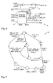
- FIG. 6 shows a block diagram of the input 20.
- the input 20 has an input control 70 whose ports are specified in more detail in FIG.
- the task of the input controller 70 is to guarantee a data transfer.
- the input controller 70 is implemented as an AFSM operating in burst mode.
- the input controller responds to incoming request signals and, by means of a signal REQ_INT, initiates the delivery of a clock signal for each incoming request signal.
- a signal ST is activated (time-out).
- the input controller is configured to respond to two possible events: the first possible event is the termination of the expected number of internal clock cycles, indicated by a STOP signal. Thereby, the input controller 70 is reset in its initial state.
- the second possible event is the arrival of a request signal during the output of remaining data in the pipeline. In this case, an already started local clock cycle must be safely terminated and the control of the clock signal must be passed to the request signal.
- the input controller 70 is connected to a circuit that follows a "wide" four-phase handshake protocol.
- the input controller 70 does not transition to a clock using the request signal until one-half of a clock cycle after the previous transition of the request signal.
- the further circuit elements shown in FIG. 6 serve to suppress an acknowledgment signal ACK_INT generated by the output 22 during local clock equalization with the aid of the clock generator 26.
- ACK _ INT is enabled when transitioning from local timing to the mode driven by the request signal. This is done by activating a signal ACK_EN.
- a flip-flop 72 is provided to generate a signal DATAV_IN intended for delivery to the locally synchronous module 12, which indicates that currently valid data is present at the input of the locally synchronous module 12.
- Z0 and Z1 are internal signals ensuring error-free operation of the input controller 70.
- FIG. 8 shows a block diagram of the output 22.
- the output 22 has an output controller 80 in the form of an asynchronous fine state machine (AFSM) and two flip-flops 82 and 84.
- the flip-flops 82 and 84 serve to condition the signals indicating that output data is valid ( DOV ) or non-valid (DONV) in order to continue to use these signals in the output controller 80.
- DOV asynchronous fine state machine
- DONV non-valid
- the output control can be excited by two mutually exclusive sources: with the aid of the internal request signal REQ_INT and with the aid of the local clock signal LCLKM. If there is no valid data at output 20, that is, DONV is activated , any request signal that is indicated either by activation of the REQ_INT or LCLKM will be activated immediately by activating the signal ACK_INT . If output data needs to be transferred to the next GALS block, that is, the DOV is enabled, an output handshake must be performed using the REQ_B and ACK_B signals. In this case, the internal handshake (signals REQ_INT and ACK_INT) must be coupled to the output handshake (signals REQ_B and ACK_B) .
- the local clock generator When both DOV is asserted and the LCKLM signal is present, the local clock generator must be delayed by means of the REQl 2 and ACKl 2 signals until an output handshake is performed. This prevents a new clock cycle from breaking before the data transfer at the output is completed.
- Z0 is an internal signal added for safe operation of the AFSM .
- the output port 22 described here is of the "push” type.
- the structure of a "pull” type output port would be very similar.
- FIG. 10 shows the result of a simulation of the operation of the asynchronous envelope circuit of FIG. 2 for different operating modes.
- a 21-stage FIFO register was selected as locally synchronous module 12.
- the simulated overall system consists of three GALS blocks connected in series.
- FIG. 10 shows the time profiles of various signals. In the top row of the timing of the signal CLK INT _ is illustrated by way of a temporal waveform 90th
- the signal INT_CLK occurs within a respective asynchronous envelope circuit. It can be seen here that the signal INT_CLK arises from the signals LCLKM and REQ_A , as has already been explained in connection with FIG. In normal operating mode, a handshake takes place on the lines REQ_A and ACK_A.
- Each request signal is interpreted as a new clock cycle.
- the envelope waits for a time-out to occur. During the wait, the internal clock signal generation is turned off. The occurrence of a time-out is activated with a signal ST . This causes the activation of the local clock signal LCLKM, which in turn drives the signal INT_CLK . If the signal REQ_A 94 indicates the arrival of new data before disabling LCLKM , a transition is initiated. In this mode, a local clock cycle is completely terminated, and then control of the internal clock signal is applied to request line REQ_A 94. Finally, it goes to normal operation, which prevailed at the beginning.
- FIG. 11 shows as an exemplary embodiment of a GALS system a baseband processor for a chip-integrated wireless broadband communication system in the 5 GHz band according to the standard IEEE 802.11a.
- This standard specifies a broadband communication system using OFDM (Ortho-Frequency Division Multiplexing) with data rates in the range of 6 to 54 Mbit / s.
- the baseband transmitter shown in FIG. 11 has three GALS blocks 100, 102 and 104. Each of the GLS blocks 100, 102 and 104 is assigned an asynchronous wrapper, which is not shown here in the functional representation of the baseband transmitter. The division of the blocks follows considerations regarding the functionality and complexity of the functional blocks of the baseband transmitter.
- the first GALS block 100 includes an input buffer 106, a scrambler 108, a signal field generator 110, an encoder 112, an interleaver 114, and a QAM mapper 116. Said blocks 106 to 116 are known per se to the person skilled in the art. The most extensive blocks of the GALS block 100 are the interleaver 114 and the mapper 116.
- the second GALS block includes a pilot channel insertion unit 118 and a pilot scrambler 120.
- the third GALS block 104 includes a block 122 for performing the inverse fast Fourier transform, a gard interval insertion unit 124, and a preamble insertion unit 126.
- the IFFT unit 122 consumes about 85% of the circuitry overhead of GALS block 3.
- the described synchronous blocks 100, 102 and 104 with their sub-blocks 106 to 126 are constructed in a data flow style (token flow).
- One problem is that the third block 104 must provide output data at a fixed speed for forwarding to a digital-to-analog converter (not shown). This is accomplished by tuning the local oscillator of block 104 to a frequency slightly greater than the fixed clock frequency of the digital-to-analog converter. The output data is then practically extracted from the locally synchronous block 104 at the desired frequency of the digital-to-analog converter by means of the ACK signal.
- a test revealed a data throughput of about 100 Msps between GALS block 104 and external synchronous environment 128.
Landscapes
- Engineering & Computer Science (AREA)
- Theoretical Computer Science (AREA)
- Physics & Mathematics (AREA)
- General Engineering & Computer Science (AREA)
- General Physics & Mathematics (AREA)
- Information Transfer Systems (AREA)
- Synchronisation In Digital Transmission Systems (AREA)
- Data Exchanges In Wide-Area Networks (AREA)
- Stabilization Of Oscillater, Synchronisation, Frequency Synthesizers (AREA)
Description
- Die Erfindung betrifft eine asynchrone Hüllschaltung für eine global asynchrone, lokal synchrone (GALS) Schaltung. Sie betrifft weiterhin eine GALS-Schaltung und ein Verfahren zum Takten eines intern synchronen Schaltungsblocks.
- Hochintegrierte Halbleiterbauelemente für die drahtlose Kommunikation beinhalten heute digitale wie analoge Schaltkreise zur Daten- und Signalverarbeitung auf einem Chip. Digitale signalverarbeitende Schaltungen werden mit Hilfe dezidieter datenpfad-orientierter Schaltungen implementiert. Alternativ ist eine Implementierung mit einem DSP (Digitaler Signal-Prozessor) möglich. Ein System mit Datenpfad-Architektur weist typischerweise komplexe Schaltkreisblöcke auf, die aufwendige arithmetische oder trigonometrische Operationen durchführen. In einem 5 GHz-Modem für den drahtlosen Betrieb in einem LAN (local area network) entsprechend dem Standart IEEE 802.11a sind beispielsweise ein FFT/IFFT (fast fourier transform/ invertide FFT)-Prozessor, ein Viterbi-Dekodierer, ein CORDIC-Prozessor sowie Kreuz- und Autokorrelatoren enthalten. Die Kommunikation zwischen diesen Blöcken erfolgt mit hohen Datenraten. Dabei folgen häufig Perioden langer Inaktivität auf Zeitabschnitte mit hohem Datendurchsatz.
- Ein wesentliches technisches Problem moderner ASICs (application specific integrated circuits) ist die Synchronisierung der unterschiedlichen, auf einem Chip integrierten Funktionsblöcke. Die Verwendung eines globalen Zeittaktes für alle Funktionsblöcke ist im Design nur mit großem Aufwand zu verwirklichen. Darüber hinaus erzeugt ein synchroner, globaler Zeittakt erhöhte elektromagnetische Interferenz (EMI). Dies erschwert die Integration analoger und digitaler Schaltungen auf einem Chip.
- Zur Lösung der oben genannten Probleme wurden in jüngerer Zeit so genannte global asynchrone lokal synchrone (GALS) Schaltungsarchitekturen vorgeschlagen. Synchron arbeitende Schaltungen triggem alle Speicheroperationen gemäß einem gemeinsamen Zeitraster, das durch den Status eines globalen Signals definiert wird. Dieses Signal wird als Takt bezeichnet. Üblicherweise wird die Anstiegsflanke des Takt-Signals zum Triggern von Speicheroperationen verwendet. Der Nachteil synchron arbeitender Schaltungen besteht darin, dass die Grundannahme, dass das Takt-Signal allen Schaltungsteilen zum selben Zeitpunkt - also synchron - zur Verfügung steht, in der Realität nicht zutrifft. Dies ist durch die Signal-Ausbreitungszeit bedingt.
- Asynchrone Schaltungen verzichten auf ein Zeitraster mit diskreten Zeitschritten. Die Funktion asynchroner Schaltungen basiert auf dem Eintreten von Ereignissen. Der momentane Zustand der Schaltung wird vollständig durch die Polarität von Signaländerungen und deren Reihenfolge bestimmt.
- GALS-Schaltungen weisen Schaltungsblöcke auf, die intern synchron arbeiten. Diese lokal synchronen Schaltungsblöcke kommunizieren miteinander in asynchroner Weise, das heißt, mit Hilfe eines Handshake-Protokolls. Daher entfällt die Notwendigkeit, die einzelnen lokal synchronisierten Schaltungsblöcke auch global miteinander zu synchronisieren. Solange jeder einzelne lokal synchrone Block dem Handshake-Protokoll folgt, können diese Schaltungsblöcke in beliebiger Weise mit einander kombiniert werden.
- Eine GALS-Architektur zeichnet sich durch eine modulare Struktur aus, die eine hohe Flexibilität des Schaltungsdesigns ermöglicht. Denn da die Schnittstelle zu jedem lokal synchronen Schaltungsmodul asynchron ist, können beliebige synchrone Schaltungen miteinander integriert werden. Jeder lokal synchrone Schaltungsblock kann ein Zeitraster mit individueller TaktSignalfrequenz aufweisen.
- Zur Umsetzung der asynchronen Kommunikation zwischen den lokal synchronen Schaltungsblöcken weisen diese jeweils eine asynchrone Hüllschaltung auf, die auch als "asynchronous wrapper" bezeichnet wird. Eine asynchrone Hüllschaltung weist Eingangs- und Ausgangsports sowie einen lokalen Takt-Signalgenerator auf. Jeder Port der Hüllschaltung, das heißt, jeder Eingang und jeder Ausgang weist eine zugehörige Port-Steuerung auf, die für die Umsetzung des Handshake-Protokolls zuständig ist. Port und Steuerung bilden zusammen eine Eingangs- bzw. Ausgangseinheit.
- Der Taktsignal-Generator einer asynchronen Hüllschaltung ist zur Erzeugung des Takt-Signals mit einer in einem bestimmten Frequenzbereich abstimmbaren Signalfrequenz ausgebildet. Ein wichtiges Merkmal von Takt-Signal-Generatoren für asynchrone Hüllschaltungen ist, dass die Erzeugung des Takt-Signals aussetzbar (pausable) ist.
- In der Schrift Jens Muttersbach et al, "Practical Design of Globally-Asychronous Locally-Synchronous Systems", Advanced Research in Asynchronous Circuits and Systems, IEEE, April 2000 wird der Entwurf von GAL-Schaltungen mit aussetzbaren Takten beschrieben.
- Shengxian Zhuang et al, beschreiben in ihrem Artikel "Asychronous Data Communication with Low Power for GALS Systems", IEEE, September 2002 eine Hüllschaltung mit "stretchable" intemem Takt und die Verlustleistungsoptimierung mit einem "low-swing" bus.
- Aus der Schrift Tormod Njolstad et al, "A Socket Interface for GALS using Locally Dynamic Voltage Scaling for Rate-Adaptive Energy Saving", IEEE, September 2001 ist eine Hüllschaltung mit Anpassung des lokalen Taktes an die erforderliche Datenverarbeitungsrate und das Aussetzen des lokalen Taktes mit einem "timer" bekannt.
- Aus der Schrift David S. Bormann, Peter Y. K. Cheoung, Asynchronous Wrapper for Heterogeneous Systems, In Proc. International Conf. Computer Design (ICCD), October 1997, Seiten 307 bis 314 ist eine asynchrone Hüllschaltung mit einer Eingangseinheit, einer Ausgangseinheit und einem Taktsignalgenerator bekannt. Gleichzeitig beschreibt diese Schrift ein Verfahren zum Takten eines intern synchronen Schaltungsblocks einer integrierten Schaltung mit Hilfe einer asynchronen Hüllschaltung. Eingangseinheit oder Ausgangseinheit erzeugen und senden ein "Stretch"-Signal an den Taktsignalgenerator, wenn am Eingang ein Anforderungssignal eines benachbarten vorangehenden Schaltungsblocks empfangen wurde bzw. am Ausgang ein Anforderungssignal an einen benachbarten nachfolgenden Schaltungblock gesendet wurde. Das "Stretch"-Signal liegt an einem Steuereingang des Taktsignalgenerators an, bis ein Handshake zum Datenaustausch mit einer benachbarten Schaltung erfolgt ist. Solange das Stretch-Signal anliegt, wird die Abgabe des nächsten Taktsignals vom Taktsignalgenerator an den synchronen Schaltungsblock verzögert. Auf diese Weise können Schaltungsblöcke individuell intern synchron getaktet werden und zugleich asynchron mit Schaltungsblöcken der Umgebung Daten austauschen.
- Nachteilig ist, dass diese asynchrone Hüllschaltung für nicht näher spezifizierte Anwendungen ausgelegt ist und daher nicht an im Einzelfall vorgegebene Schaltungs-Umgebungen angepasst ist. Dies gilt insbesondere mit Blick auf für einen GALS-Block erforderliche Leistungsaufnahme. Mechanismen zum Verringern der Leistungsaufnahme sind mit den bekannten asynchronen Hüllschaltungen nur schwer zu realisieren.
- Das der vorliegenden Erfindung zugrunde liegende technische Problem ist es, eine asynchrone Hüllschaltung anzugeben, die die Realisierung eines GALS-Blocks mit geringer Leistungsaufnahme ermöglicht.
- Gemäß einem ersten Aspekt der Erfindung wird als Lösung des technischen Problems eine asynchrone Hüllschaltung angegeben mit mindestens einer Eingangseinheit, die ausgebildet ist, ein Anforderungssignal von extern zu empfangen und den Empfang des Anforderungssignals durch Abgabe eines zugeordneten Bestätigungssignals nach extern anzuzeigen, einer aussetzbaren Takteinheit, die ausgebildet ist, ein erstes Taktsignal wiederholt zu erzeugen und an einen der asynchronen Hüllschaltung zugeordneten, intern synchronen Schaltungsblock abzugeben, wobei die Eingangseinheit ausgebildet ist, auf den Empfang eines Anforderungssignals hin ein mit dem Anforderungssignal in definierter zeitlicher Beziehung stehendes zweites Taktsignal zu erzeugen und an den intern synchronen Schaltungsblock abzugeben, und wobei eine mit der Eingangseinheit verbundene Timeout-Einheit vorgesehen ist, die ausgebildet ist, die Abgabe des ersten Taktsignals zu unterdrücken.
- Die Erfindung beruht auf der Erkenntnis, dass ein GALS-Block zur Verarbeitung eines kontinuierlichen Datenstroms in einem quasi-synchronen Betrieb am effektivsten arbeitet. Ein quasi-synchroner Betrieb lässt sich erfindungsgemäß realisieren, in dem ein GALS-Block in einem von Anforderungssignalen angetriebenen ("request driven") Betriebsmoduls betrieben wird. Der intern synchrone Schaltungsblock wird demnach immer dann getaktet, wenn tatsächlich Daten an seinem Eingang eintreffen. Anforderungssignale gehen bei einer asynchronen Hüllschaltung von extern, d.h., von einer benachbarten, im Datenfluss vorangehenden asynchronen Hüllschaltung ein, wenn Daten zur Eingabe an den lokalen, intern synchronen Schaltungsblock vorliegen.
- Der Grundgedanke der erfindungsgemäßen Vorrichtung ist demnach in der Eingangseinheit verwirklicht, die zur Abgabe eines (im Anspruchswortlaut nur zur Unterscheidung als "zweites" benanntes) Taktsignals in definierter zeitlicher Beziehung zum eingegangenen Anforderungssignal ausgebildet ist. Die erfindungsgemäße Vorrichtung kann grundsätzlich auch ohne aussetzbare Takteinheit und ohne Time-out Einheit arbeiten. Dies hat zur Folge, dass sie allein mit Hilfe der zweiten Taktsignale getaktet wird. In Abwesenheit von Anforderungssignalen würde die lokal synchrone Schaltung in diesem Fall nicht getaktet. Dies hat zwar den Nachteil, dass in der Pipeline der synchronen Schaltung verbliebene Daten nicht ausgegeben werden. Doch mit einem erneuten Eintreffen von Anforderungssignalen würde die Ausgabe fortgesetzt. Die intern synchrone Schaltung wird zur Vermeidung dieses Nachteils gemäß Anspruch 1 mit Hilfe zweier alternativer Quellen getaktet, entweder mit Hilfe der Takteinheit, oder mit Hilfe der Eingangseinheit aufgrund von Anforderungssignalen. Man könnte auch von einem "Multiplexen" der ersten und zweiten Taktsignale sprechen. Die mit eingehenden Anforderungssignalen synchronisierte Taktung durch die "zweiten" Taktsignale hat grundsätzlich Priorität gegenüber der Taktung mit Hilfe "erster" Taktsignale von der Takteinheit. Dabei wird jedoch gewährleistet, dass eine Taktperiode eines "ersten" Taktsignals beendet wird, bevor ein "zweites" Taktsignal an den intern synchronen Schaltungsblock abgegeben wird.
- Erfindungsgemäß wird ein zweites Taktsignal mit einem aktuell empfangenen Anforderungssignal synchronisiert, indem das zweite Taktsignal in definierter zeitlicher Beziehung zum Anforderungssignal erzeugt wird. Die definierte zeitliche Beziehung kann beispielsweise bedeuten, dass Anstiegsflanke und abfallende Flanke des zweiten Taktsignals in festem zeitlichen Abstand zur Anstiegsflanke und abfallenden Flanke des Anforderungssignals erzeugt werden. Bei Eintreffen eines Anforderungssignals, das im Rahmen eines kontinuierlichen Datenstroms eingeht, wird auf eine Taktung mit einem Taktsignal durch einen eigens vorgesehenen Taktgenerator verzichtet. Ein solcher Taktgenerator ist dennoch Bestandteil der asynchronen Hüllschaltung nach Anspruch 1, um bei Bedarf auch ohne anliegendes Anforderungssignal den intern synchronen Schaltungsblock antreiben zu können.
- Die erfindungsgemäße Anordnung hat verschiedene Vorteile. Sie ermöglicht zunächst einen Verzicht auf einen globalen Taktbaum. Liegen keine Anforderungssignale von extern vor, ermöglicht die erfindungsgemäße Anordnung eine Taktung mit Hilfe der ersten Taktsignale nur bei Bedarf, also beispielsweise solang Daten zur Abgabe nach extern in der Pipeline der intern synchronen Schaltung vorhanden sind. Die erfindungsgemäße asynchrone Hüllschaltung ermöglicht daher eine geringe, am tatsächlichen Datenverarbeitungsbedarf orientierte Leistungsaufnahme eines GALS-Blocks. Weiterhin bestehen bei der Anordnung nach Anspruch 1 aufgrund der von Anforderungssignalen abhängigen Taktung nur wenige Randbedingungen für die Taktfrequenz des lokalen Taktgenerators, der die "ersten" Taktsignale erzeugt. Die Taktfrequenz eines lokalen Taktgenerators muss insbesondere nicht der Datenrate angepasst sein. Dies erlaubt eine einfache Gestaltung des Ringoszillators des lokalen Taktgenerators.
- Bei einer ersten Ausführungsform der Erfindung ist die Timeout-Einheit ausgebildet, mit Ablauf einer vorbestimmten Zeitspanne nach Abgabe des letzten zweiten Taktsignals ein Steuersignal zum Freischalten der Abgabe des ersten Taktsignals abzugeben. Bei dieser Ausführungsform wird nach dem letzten Anforderungssignal eine so genannte Time-Out-Zeitspanne abgewartet, bevor die Taktung durch den lokalen Taktgenerator die Taktung durch eingehende Anforderungssignate ersetzt. Dies hat zum einen den Vorteil, dass die Tak- ' tung nicht unkontrolliert zwischen dem ersten und zweiten Taktsignal hin- und herspringt, wenn nur kurzzeitig kein Anforderungssignal anliegt. Zum anderen wird mit der Freischaltung des ersten Taktsignals ermöglicht, unabhängig vom Vorliegen eines Anforderungssignals die Pipeline der lokalen, intern synchronen Schaltung zu leeren und damit einen zusammenhängenden Datenfluss über mehrere GALS-Blöcke als solchen zu erhalten.
- Eine zur ersten Ausführungsform alternative, zweite Ausführungsform beruht auf dem Gedanken, anstelle des Abwartens einer bestimmten Zeitspanne mit Hilfe der Time-Out-Einheit eine Ergänzung des Kommunikationsprotokolls zwischen den asynchronen Hüllschaltungen benachbarter GALS-Blöcken vorzusehen. Mit einem entsprechenden Signal zeigt bei dieser alternativen Ausführungsform die asynchrone Hüllschaltung des vorangehende GALS-Blocks an, dass ein aktuelles Anforderungssignal das vorerst letzte Anforderungssignal ist. Bei dem Signal kann es sich um ein modifiziertes Anforderungssignal oder um ein separates, parallel mit einem Anforderungssignal zu übersendendes Signal handeln. Zum Aussenden des Signals kann beispielsweise die Ausgangseinheit der asynchronen Hüllschaltung ausgebildet sein. Die entsprechende schaltungstechnische Umsetzung ist dem Fachmann an sich bekannt. Die Eingangseinheit ist entsprechend zum Empfang des Signals ausgebildet. Sie kann auch die in der ersten Ausführungsform von der TimP-Out-Einheit ausgeübte Funktion der Abgabe des Freischaltsignals für das erste Taktsignal wahrnehmen.
- Zur Optimierung der Leistungsaufnahme sollte in der ersten wie der zweiten Ausführungsform eine Taktung mit Hilfe des ersten Taktsignals nur so lange erfolgen, wie Daten in der Pipeline vorhanden sind. Bevorzugt ist daher eine mit der Takteinheit und mit der Eingangseinheit verbundene Taktsteuereinheit vorgesehen, welche ausgebildet ist, die Takteinheit zur Abgabe einer Anzahl von Taktimpulsen anzutreiben, wobei die Anzahl der Taktimpulse kleiner oder gleich der Tiefe einer Pipeline des zugeordneten, intern synchronen Schaltungsblockes ist. Auf diese Weise kann die Taktung der intern synchronen Schaltung nach Leeren der Pipeline unterbrochen werden, bis erneut Anforderungssignale vorliegen.
- Zum Aussetzen oder Unterbrechen der Taktung mit Hilfe des ersten Taktsignals ist die Taktsteuereinheit bevorzugt ausgebildet, der Takteinheit nach Abgabe der genannten Anzahl von Taktimpulsen ein Steuersignal zum Anhalten zu senden.
- Die Eingangseinheit ist bei der erfindungsgemäßen asynchronen Hüllschaltung vorzugsweise ausgebildet, bei Anliegen eines Anforderungssignals ein Steuersignal an den intern synchronen Schaltungsblock zum Freischalten einer Dateneingabe abzugeben. Es können mehrere Eingangseinheiten vorgesehen sein. Dies ist beispielsweise sinnvoll, wenn der GALS-Block eingangsseitig mit mehreren anderen GALS-Blöcken verbunden ist.
- Ebenso können eine oder mehrere Ausgangseinheiten vorgesehen sein, die ausgebildet sind, ein Anforderungssignal nach extern zu senden und auf den Empfang eines Bestätigungssignals von extern hin ein Steuersignal an den intern synchronen Schaltungsblock zum Freischalten einer Datenausgabe abzugeben.
- Bevorzugt erfolgt die Kommunikation zwischen einer Ausgangseinheit eines ersten GALS-Blocks einerseits und einer verbundenen Eingangseinheit eines zweiten GALS-Blocks über ein dem Fachmann an sich bekanntes vierphasiges Handshake-Protokoll. Die Eingangseinheit und die Ausgangseinheit sind bevorzugt jeweils ausgebildet, mit Hilfe des vierphasen Handshake-Protokolls zu kommunizieren.
- Mit Hilfe der erfindungsgemäßen asynchronen Hüllschaltung lassen sich GALS-Blöcke mit einem intern synchronen Schaltungsblock und einer asynchronen Hüllschaltung realisieren. Aus verschiedenen solcher GALS-Blöcke lassen sich in hochintegrierten Schaltungen GALS-Architekturen realisieren, umfassend mindestens einen intern synchronen Schaltungsblock und je eine zugeordnete asynchrone Hüllschaltung.
- In einem erfindungsgemäßen GALS-Block ist vorzugsweise einem Dateneingang des intern synchronen Schaltungsblocks ein Daten-Latch vorgeschaltet ist, dessen Betrieb von der Eingangseinheit gesteuert wird. Dieser dient zum einen in bekannter Weise zum Puffern eingehender Daten. Zum andern verhindert der Daten-Latch das Auftreten metastabiler Zustände am Eingang des intern synchronen Schaltungsblocks.
- Gemäß einem zweiten Aspekt der Erfindung wird zur Lösung des oben genannten Problems ein Verfahren zum Takten eines intern synchronen Schaltungsblocks einer integrierten Schaltung mit Hilfe einer asynchronen Hüllschaltung vorgeschlagen, wobei der intern synchrone Schaltungsblock mit Hilfe eines ersten Taktsignals getaktet werden kann, das ein lokaler Taktsignalgenerator erzeugen kann. Das erfindungsgemäße Verfahren hat folgende Schritte:
- a) Aussetzen der Abgabe des ersten Taktsignals oder Abschalten des lokalen Taktgenerators
- b) Warten auf den Empfang eines Anforderungssignals von extern am Eingang der asynchronen Hüllschaltung
- c) Abgabe eines zweiten Taktsignals von der asynchronen Hüllschaltung an den intern synchronen Schaltungsblock in definierter zeitlicher Beziehung zum Empfang des Anforderungssignals und ohne Hilfe des lokalen Taktsignalgenerators,
- d) Warten auf den Empfang eines nächsten Anforderungssignals von extern und gegebenenfalls Wiederholen des vorangegangenen Schrittes.
- Das erfindungsgemäße Verfahren bricht mit dem im Zusammenhang mit GALS-Architekturen gängigen asynchronen Taktverfahren, bei dem das lokale Taktsignal bedarfsweise verzögert werden kann. Es schlägt an Stelle dessen eine am Vorliegen eines Anforderungssignals orientierte Taktung vor. Das lokale (erste) Taktsignal wird ausgesetzt oder der lokale Taktsignalgenerator wird abgeschaltet. Aus einem eintreffenden externen Anforderungssignal wird ein Taktsignal, das im Kontext der vorliegenden Anmeldung als "zweites Taktsignal" bezeichnet wird, für den lokal synchronen Block direkt abgeleitet.
- Der lokale Taktgenerator dient ausschließlich dazu, interne Pipelinestufen der lokal synchronen Schaltung zu leeren, wenn über einen bestimmten Zeitraum kein externes Anforderungssignal anliegt. Die Vorteile des Verfahrens ergeben sich unmittelbar aus dem zur erfindungsgemäßen asynchronen Hüllschaltung Gesagten.
- Ein Ausführungsbeispiel des erfindungsgemäßen Verfahrens beinhaltet bei Ausbleiben eines Anforderungssignals über eine vorbestimmbare Zeitspanne ein Umschalten auf die Abgabe des mit Hilfe des lokalen Taktsignalgenerators erzeugten ersten Taktsignals. Bei diesem Ausführungsbeispiels wird der lokale Taktsignalgenerator bevorzugt nach Leeren einer Pipeline des intern synchronen Schaltungsblocks oder nach dem Eintreffen eines neuen Anforderungssignals wieder abgeschaltet. Die Vorteile dieser Ausführungsbeispiele des erfindungsgemäßen Verfahrens ergeben sich ebenfalls aus der Beschreibung der erfindungsgemäßen Vorrichtung.
- Weitere Merkmale und Vorteile der Erfindung werden nachfolgend anhand der Beschreibung von Ausführungsbeispielen anhand der beiliegenden Figuren verdeutlicht. Es zeigen:
- Figur 1
- ein Blockschaltbild eines Ausführungsbeispieles einer asynchronen Hüllschaltung,
- Figur 2
- ein detailliertes Blockschaltbild der asynchronen Hüllschaltung aus Figur 1,
- Figur 3
- ein Schaltbild des Takt-Signal-Generators aus Figur 2,
- Figur 4
- ein Schaltdiagramm der Takt-Steuerung aus Figur 2,
- Figur 5
- ein Blockschaltbild des Time-Out-Detektors aus Figur 2,
- Figur 6
- ein Blockdiagramm des Eingangs der Hüllschaltung aus Figur 2,
- Figur 7
- eine Spezifizierung einer Eingangssteuerung des Eingangs der Hüllschaltung aus Figur 2,
- Figur 8
- ein Blockdiagramm des Ausgangs der Hüllschaltung der Figur 2,
- Figur 9
- eine Spezifizierung einer Ausgangssteuerung des Ausgangs der Figur 8,
- Figur 10
- ein Diagramm mit einer Darstellung des zeitlichen Verlaufs verschiedener Signale in unterschiedlichen Betriebsarten der asynchronen Hüllschaltung und
- Figur 11
- ein Blockschaltbild eines Anwendungsbeispiels in Form eines Basisband-Senders für die drahtlose Kommunikation
- Figur 1 zeigt ein vereinfachtes Blockdiagramm einer Schaltung 10, die einen lokal synchronen Block 12 und eine asynchrone Hüllschaltung 14 aufweist. Der lokal synchrone Block 12 hat hier nicht näher beschriebene Eingänge und Ausgänge für Daten, die mit benachbarten Schaltungsblöcken ausgetauscht werden. Dies ist durch Pfeile 16 und 18 symbolisiert.
- Die asynchrone Hüllschaltung der Schaltung 10 hat einen Eingang 20 zum Empfangen und Aussenden von Handshake-Signalen. Der Eingang kommuniniziert mit Hilfe der Handshake-Signale beispielsweise mit einem Ausgang einer im Datenfluss vorangehenden, benachbarten, gleichartigen asynchronen Hüllschaltung, die nicht dargestellt ist. Mit dem Eingang 20 verbunden ist ein Ausgang 22, der in analoger Weise Handshake-Signale mit der Umgebung austauscht. Beispielsweise kommuniziert der Ausgang 22 mit einem Eingang einer im Datenfluss nachfolgenden, benachbarten, gleichartigen asynchronen Hüllschaltung, die ebenfalls nicht dargestellt ist. Ein Time-Out-Detektor 24 ist einerseits mit dem Eingang 20 und andererseits mit einem Takt-Signalgenerator 26 verbunden. Die Verbindung des Takt-Signalsgenerators 26 mit dem Time-Out-Detektor 24 erfolgt über Steuereingänge. Ebenso ist der Takt-Signalgenerator 26 mit dem Ausgang 22 über Steuerein- und -ausgänge verbunden.
- Die Verbindung des lokal synchronen (in dieser Anmeldung auch als intern synchron bezeichneten) Blocks 12 mit der asynchronen Hüllschaltung 14 erfolgt über Steuerleitungen 28 und 30. Über die Steuerleitungen 28 und 30 werden dem lokal synchronen Block 12 ein Takt-Signal des Takt-Signalgenerators 26 bzw. Anforderungssignale externer Schaltungen vom Eingang 20 her zugeleitet.
- Die lokal synchrone Schaltung 12 wird demnach sowohl von eingehenden Anforderungssignalen externer Schaltungen als auch durch das lokale Takt-Signal angetrieben. Ein Anforderungssignal, das über den Eingang 20 geleitet wird, stammt von einer asynchronen Hüllschaltung eines benachbarten Schaltungsblockes. Es ist mit Daten synchronisiert, die den lokal synchronen Block 12 über die Datenleitung 16 erreichen.
- Das hinter dem vorliegenden Ausführungsbeispiel stehende Konzept beruht auf einem verteilten Steuerungsmechanismus, der als Datenfluss-Ansatz (Token Flow Approach) bezeichnet wird. Jeder lokal synchrone Block 12 verschiedener in einem System zusammengefasster Schaltungen 10 weist eine eigene asynchrone Hüllschaltung auf. Diese asynchrone Hüllschaltung sendet zusätzlich Signale an benachbarte Hüllschaltungen, die über den momentanen Zustand der Hüllschaltung Auskunft geben. Als Token wird in diesem Zusammenhang die Kombination einer Dateneinheit mit einer Information zur Gültigkeit dieser Dateneinheit bezeichnet. Die benachbarten Hüllschaltungen betreiben ihren jeweiligen lokal synchronen Block 12 in Abhängigkeit von diesem Signal. Zusätzlich erzeugen die Module, die zu einem lokal synchronen Block gehören, ein weiteres Signal zur Übersendung an das funktionell nachfolgende Modul, das das Betriebsende anzeigt. In Abhängigkeit von diesem Signal akzeptiert das Modul die Daten des vorhergehenden Moduls und verarbeitet sie.
- Liegt für eine vorbestimmte Zeitspanne kein Anforderungssignal am Eingang 20 an, wechselt die Hüllschaltung 14 in einen anderen Zustand, in dem sie interne Takt-Signale mit Hilfe eines weiter unten näher beschriebenen lokalen Ringoszillators erzeugt. Die Anzahl der intern erzeugten Takt-Signale wird so festgesetzt, dass sie gleich der Anzahl der Taktzyklen ist, die benötigt werden, um die Pipeline der lokal synchronen Schaltung 12 zu leeren. Sobald keine gültigen Daten mehr im synchronen Block sind, hält der Takt-Signalgenerator 26 an. Der lokal synchrone Block 12 ist anschließend inaktiv, bis ein nächstes Anforderungssignal eintrifft.
- Das Eintreffen eines Anforderungssignals wird an einer Änderung des Zustandes am Eingang 20 detektiert. Üblicherweise wird hierbei der Nachweis einer ansteigenden Signalflanke als Eintreffen eines neuen Anforderungssignals interpretiert.
- Wird am Eingang 20 ein Anforderungssignal detektiert, während der lokal synchrone Block nach Detektion eines Time-Outs vom lokalen Takt-Signalgenerator angetrieben wird, muss zunächst der aktuelle Takt-Zyklus beendet werden, um Metastabilität an den Dateneingängen des lokal synchronen Blocks 12 zu verhindern. Anschließend kann die Takt-Signalerzeugung vom lokalen Ringoszillator des Takt-Signalgenerators 26 auf die Eingangsleitung 30 übergeben werden. Zur Vermeidung von Metastabilität in der Handhabung dieser Situation sind weitere Schaltungen erforderlich, die weiter unten näher beschrieben werden.
- Die hier vorgeschlagene Schaltungsarchitektur hat zahlreiche Vorteile. Wie in jedem GALS-System ist zunächst kein globaler Takt-Baum erforderlich. Das Takt-Signal wird durch ein "Multiplexen" des lokalen Takt-Signals und der Anforderungssignale erzeugt. Auf Grund des von Anforderungssignalen angetriebenen Betriebs muss die Frequenz des lokalen Takt-Signalgenerators nicht präzise mit der Frequenz eines globalen Takt-Signalgenerators oder mit der Datenrate übereinstimmen. Dies verringert die Zahl der Randbedingungen für das Design des Ringoszillators: Die vorliegende Implementierung erfordert weiterhin keine große Registerkapazität für Eingangsdaten im lokal synchronen Block 12. Dadurch wird eine unerwünschte Verzögerung vermieden und zugleich die Hardwarestruktur des Systems vereinfacht. Der lokal synchrone Block 12 antwortet bei dem hier vorgesehenen Konzept unmittelbar auf Anforderungssignale und vermeidet so Verzögerungen.
- Ein weiterer Vorteil der Verwendung eines Datenfluss-Ansatzes in dem hier vorgeschlagenen Schaltungskonzept besteht darin, dass anstelle lokal synchroner Pipelines ebenso vollkommen asynchrone Schaltungen verwendet werden können, wenn dies gewünscht ist.
- Schließlich bietet die vorliegende Architelctur einen effizienten Energiesparmechanismus. Ein jeweiliger synchroner Block 12 wird immer nur dann angetrieben, wenn an seinem Eingang Daten anliegen oder wenn das Austreiben der noch in der lokalen Pipeline verbliebenen Daten erforderlich ist. Zu allen anderen Zeitpunkten ist der lokal synchrone Block 12 außer Betrieb.
- Figur 2 zeigt ein detailliertes Blockdiagramm des GALS-Blocks aus Figur 1. Die asynchrone Hüllschaltung 14 weist zusätzlich zu den in Figur 1 gezeigten Elementen eine Takt-Steuerung 32 und ein transparentes Latch 34 auf.
- Die Funktion der asynchronen Hüllschaltung 14 wird nachfolgend anhand der Figuren 2 bis 9 in näheren Details erläutert. In Figur 2 sind neben den funktionellen Blöcken auch ihre Verbindungen sowie die auf den Verbindungen übertragenen Signale dargestellt. Die Verbindungslinien zeigen durch die Pfeilrichtung die Übertragungsrichtung der Signale an.
- Die Taktung des lokal synchronen Moduls 12 erfolgt mit einem Signal INT CLK. Das Signal INT_CLK ist das Ausgangssignal eines ODER-Gatters 36 an dessen Eingängen zum einen ein Signal REQ_INT und zum anderen ein Signal LCLKM anliegt. Das Signal REQ_INT wird vom Eingang 20 erzeugt, wenn von extern ein Anforderungssignal REQ_A über den Time-Out-Generator 24 in Form eines weiteren Signals REQ_A1 am Eingang empfangen wurde. Einzelheiten zur Struktur und Funktion des Time-Out-Generators 24 werden unten im Zusammenhang mit Figur 5 erläutert. Das Signal LCLKM ist das Ausgangssignal eines UND-Gatters 38, dessen zwei Eingänge zum einen mit dem Takt-Generator 26 und zum anderen mit dem Time-Out-Generator 24 verbunden sind. Die Funktion des UND-Gatters 38 besteht darin, dem Time-Out-Generator 24 durch ein Signal ST eine Steuerung der Weitergabe des Ausgangssignals LCLK des Takt-Generators 26 an das ODER-Gatter 36 zu ermöglichen.
- Die Signale REQ_INT und INT_CLK schließen einander wechselseitig aus. Aus diesem Grunde ist das INT_CLK-Signal, das das lokal synchrone Modul 12 erreicht, stets eindeutig entweder auf Grund eines Anforderungssignals von extern oder auf Grund einer vom Time-Out-Generator 24 gesteuerten Taktung durch den Takt-Generator 26 erzeugt.
- Über die Datenleitung 16 von extern eingehende Daten-Signale DATA_IN werden im transparenten Latch 34 gepuffert. Dies ist erforderlich, um einen metastabilen Zustand am Eingang des lokal synchronen Blocks zu vermeiden. Der Betrieb des Latch 34 wird mit einem Signal DLE gesteuert, wobei das Register transparent ist, wenn das Signal DLE anliegt. Das Signal DLE liegt an nach einer Signaländerung des Takt-Generators 26 wenn zuvor im Latch gespeicherte Daten schon in die Registerstufe des lokal synchronen Moduls 12 geschrieben wurden. Es ist nicht erforderlich, dass das lokal synchrone Modul 12 weitere Register aufweist. Die eingehenden Daten können direkt einem Logikblock (nicht gezeigt) zugeführt werden, der der ersten Registerstufe (ebenfalls nicht gezeigt) vorgeschaltet ist.
- Nachfolgend wird die Struktur und die Funktion des aussetzbaren Takt-Generators 26 anhand der Figur 3 näher erläutert.
- Der lokale Takt-Signalgenerator 26 hat einen Ringoszillator 39, der ein Müller-C-Element 40, eine Verzögerungsstrecke 44 und ein Oder-Gatter (mit nachgeschaltetem Inverter) 46 aufweist. Über zwei Steuereingänge erhält der Ringoszillator 29 Signale, zum einen von einem Arbiter 42 und zum anderen über einen zweiten Eingang des ODER-Gatters 46. An das ODER-Gatter 46 wird zum einen das Ausgangssignal LCLK des Ringoszillators rückgeführt. Zum anderen ist das ODER-Gatter 46 mit einem Ausgang der Takt-Steuerung 32 verbunden, über den ein Signal STOPI angelegt werden kann.
- Mit Hilfe des Signals STOPI kann der Ringoszillator 39 angehalten werden. Das STOPI-Signal liegt in zwei Fällen an: Zum einen unmittelbar nach einem Reset, um das Aktivieren des Oszillators vor dem Eintreffen des ersten Anforderungssignals bei dem lokalen Block zu verhindern. Zum anderen, nach einem Time-Out, das heißt, wenn die Anzahl der lokalen Takt-Zyklen gleich der Anzahl von Zyklen ist, die notwendig ist, alle gültigen Daten innerhalb der Pipeline auszugeben. In dieser Situation wird das lokale Takt-Signal abgeblockt, um einen unnötigen Energieverbrauch zu verhindern.
- Der Ringoszillator 39 kann drei Grund-Moden annehmen: Schlafmodus, Time-Out-Messmodus und Takt-Gemeratormodus. Im Schlafmodus blockiert ein Stopsignal STOPI den Betrieb des Takt-Generators 26. Im Time-Out-Messmodus ist der Eingangs-Handshake freigeschaltet und der Eingang wartet auf das Eintreten eines Time-Out-Ereignisses. Ein Time-Out-Ereignis ist das Fehlen eines Anfordernungssignals am Eingang für eine vorgegebene Zeitspanne (TTime-out). Der Eingangs-Handshake wartet auch auf eine Signaländerung auf der Anforderungs-Signal-Leitung. Im vorliegenden Ausführungsbeispiel ist der Takt-Generator auch zur Erzeugung eines Time-Out-Signals ausgebildet. Der Takt-Generatormodus wird aktiviert, wenn ein Time-Out eingetreten ist. Das heißt, dass der lokal synchrone Block 12 dann getaktet wird, um alle gültigen Daten in der Pipeline auszugeben.
- Figur 4 zeigt ein Blockdiagramm der Takt-Steuerung 32. Die Aufgabe der Takt-Steuerung 32 ist die Steuerung des Takt-Generators 26. Die Takt-Steuerung 32 erzeugt zwei Ausgangssignale: STOPI und STOP. Das Signal STOP ist ein Steuersignal für eine asynchrone Finite State Maschine (AFSM) einer Eingangssteuerung, die dem Eingang 20 zugeordnet ist. Hierauf wird weiter unten im Kontext der Figuren 6 und 7 näher eingegangen. Wenn das STOP-Signal anliegt, wird das lokale Takt-Signal angehalten. Das STOP-Signal wird aktiviert, wenn ein Zähler 48, der mit dem lokalen Takt-Signal getaktet wird eine Zahl erreicht, die gleich der Tiefe der synchronen Pipeline ist. Das Signal STOPI wird vom Signal STOP mit Hilfe eines zusätzlichen D-Flipflop 50 abgeleitet. Dieses Signal wird unmittelbar als Steuersignal für den Ringoszillator 39 des Takt-Generators verwendet. Das D-Flipflop dient dazu, dieses Signal im aktivierten Zustand zu halten, bis ein neues Anforderungssignal eintrifft.
- Figur 5 zeigt ein Blockschaltbild des Time-Out-Detektors 24. Der Time-Out-Detektor 24. weist einen Zähler 52 auf. Der Zähler 52 zählt die Anzahl negativer, also abfallender Flanken des lokalen Takt-Signals. Dieser Zähler ist als ein Standard-Synchronzähler ausgelegt. Wenn er seinen letzten Wert erreicht, erzeugt er ein Time-Out-Signal. Das Reset-Signal RST wird während jedes Handshakes am Input-Port einmal aktiviert. Das RST-Signal und das Takt-Signal schließen einander nicht grundsätzlich aus. Diese Tatsache bürgt das Risiko eines metastabilen Verhaltens des Zählers 52. Zur Vermeidung von Metastabilität wird ein Ausschlusselement 54 (Mutual Exclusion Element MUTEX) dem Eingang des Zählers 52 vorgeschaltet. Das MUTEX-Element löst das gleichzeitige Auftreten einer ansteigenden Flanke des Takt-Signals und einer abfallenden Flanke des Reset-Signals. Auch ein dem Mutex-Element 54 vorgeschaltetes Flipflop 60 dient dem wechselseitig ausschließenden Auftreten eines Reset und eines LCLK-Signals am Eingang des Zählers 52.
- Eine weitere problematische Situation ist das gleichzeitige Auftreten eines externen Anforderungssignals REQ_A und eines Time-Out-Signals. Ein solcher Zustand könnte den zu Grunde gelegten Burst-Modus-Betrieb verletzen und eine fehlerhafte Arbeitsweise der AFSM bewirken. Zur Lösung dieses möglichen Problems ist ein weiteres MUTEX-Element 56 vorgesehen. Um die Leitung für das Anforderungssignal REQ_A1, in Figur 5 mit dem Bezugszeichen 58 gekennzeichnet, die meiste Zeit verfügbar zu halten, sollte das Time-Out-Signal auf der Eingangsseite des MUTEX-Elementes 56 lediglich für eine sehr kurze Zeitspanne aktiv sein. Dieses Verhalten wird mit Hilfe zweier Flip-flops 62 und 63 erreicht. Der erste Flipflop 62 wird auf ein logisches "Hoch"-Signal ("1") gesetzt, wenn ein Time-Out auftritt, das heißt, wenn der Ausgang des Zählers 52 "1" ist. Wenn im Anschluss an die Arbitrierung ein Time-Out eingeleitet ist, wird der zweite Flipflop 63 getaktet. Das Takten des zweiten Flipflops 63 aktiviert das Signal ST. Dies wiederum führt zum Zurücksetzen des ersten Flipflops 62, was eine schnelle Weiterleitung eines externen Anforderungssignals REQ_A an die asynchrone Fine State Maschine (AFSM) im Eingang 20 ermöglicht.
- Figur 6 zeigt ein Blockschaltbild des Eingangs 20. Der Eingang 20 weist eine Eingangssteuerung 70 auf, deren Ports in Figur 7 näher spezifiziert sind. Aufgabe der Eingangssteuerung 70 ist es, einen sicherein Datentransfer zu garantieren. Die Eingangssteuerung 70 ist als AFSM ausgebildet, die im Burst-Modus arbeitet.
- Im normalen Betriebsmodus reagiert die Eingangssteuerung auf eingehende Anforderungssignale und initiiert mit Hilfe eines Signals REQ_INT die Abgabe eines Taktsignals für jedes eingehende Anforderungssignal.
- Wenn auf den Eingangsleitungen für eine bestimmte Zeitspanne kein Anforderungssignal anliegt, wird ein Signal ST aktiviert (Time-Out). In diesem Zustand ist die Eingangssteuerung ausgebildet, auf zwei mögliche Ereignisse zu reagieren: Das erste mögliche Ereignis ist die Beendigung der erwarteten Anzahl interner Taktzyklen, die durch ein Signal STOP angezeigt wird. Dadurch wird die Eingangssteuerung 70 in ihrem anfänglichen Zustand zurückversetzt. Das zweite mögliche Ereignis ist das Eintreffen eines Anforderungssignals während der Ausgabe restlicher Daten in der Pipeline. In diesem Fall muss ein bereits begonnener lokaler Taktzyklus sicher beendet werden und die Steuerung des Taktsignals muss an das Anforderungssignal übergeben werden. Im vorliegenden Ausführungsbeispiel ist die Eingangssteuerung 70 mit einer Schaltung verbunden, die einem "breiten" Vier-Phasen Handshake-Protokoll folgt.
- Die Eingangssteuerung 70 erzeugt einen Übergang auf eine Taktung mit Hilfe des Anforderungssignals nicht bevor die Hälfte eines Takt-Zyklus nach dem vorangehenden Übergang des Anforderungssignals.
- Die weiteren Schaltungselemente, die in Figur 6 dargestellt sind, dienen dazu, während der lokalen Taktereugung mit Hilfe des Takt-Generators 26 ein vom Ausgang 22 erzeugtes Bestätigungssignal ACK_INT zu unterdrücken. ACK_INT wird freigeschaltet, wenn von der lokalen Taktereugung wieder auf die durch das Anforderungssignal angetriebene betriebsweise übergegangen wird. Dies geschieht durch Aktivieren eines Signals ACK_EN.
- Ein Flipflop 72 ist vorgesehen, um ein für die Abgabe an das lokal synchrone Modul 12 vorgesehenes Signal DATAV_IN zu erzeugen, das anzeigt, dass aktuell gültige Daten am Eingang des lokal synchronen Moduls 12 anliegen.
- Bei dem hier beschriebenen Eingang handelt es sich um einen Eingang vom "Pull-Typ". Auf ähnliche Weise kann ein Eingang vom "Push" konstruiert werden mit nur geringfügigen, dem Fachmann bekannten Modifikationen.
- Zur ergänzenden Erläuterung des Graphs der Figur 7 ("Signal-Transition-Graph") sind nachfolgend sind die logischen Gleichungen aufgeführt, die den Ausgangssignalen der Eingangssteuerung 70 zu Grunde liegen. Dabei bezeichnet ein Hochstrich am Ende eines Signals die Inversion dieses Signals, ein Plus-Zeichen ein logisches "Oder" und ein Multiplikationszeichen ein logisches "Und".
- REQ_INT =
- REQ_A1·REQ_INT+ACKC'·REQ_INT+ REQ_A1·ACKC'·ST'·Z0'
- ACK_A =
- ACKC'·REQ_INT + ST·ACK_A + REQ_A1·RST + REQ_A 1·A CKC'·Z0 + REQ_A1·ACKC'-ST'·Z0'
- ACKEN =
- ACKI 1 + ACKC·ACKEN + ACKEN·Z0'
- RST =
- STOP + ACKC'·REQ_INT + REQ_A1·RST + ACKC'·ST·Z0 + REQ_A1·ACKC'·ST·Z0'
- REQI1 =
- REQ_A1·ST·ACKI1'·ACKEN'·Z0'
- Z0 =
- STOP+REQ_A1·Z0+ST·Z0+ACKC·ACKI1'·ACKEN
- Z1 =
- REQ_A1'·ACKC + ACKC·Z1 +REQ_A1'·ST'·Z1
- Z0 und Z1 sind interne Signale, die einen fehlerfreien Betrieb der Eingangssteuerung 70 sicherstellen.
- Nachfolgend wird anhand der Figuren 8 und 9 Struktur und Funktion des Ausgangs 22 erläutert. Figur 8 zeigt ein Blockdiagramm des Ausgangs 22. Der Ausgang 22 weist eine Ausgangssteuerung 80 in Form einer asynchronen Fine State Maschine (AFSM) und zwei Flip-Flops 82 und 84 auf. Die Flip-Flops 82 und 84 dienen dazu, die Signale zu konditionieren, die anzeigen, dass Ausgangsdaten gültig (DOV) oder nicht gültig (DONV) sind, um diese Signale entsprechend in der Ausgangssteuerung 80 weiterverwenden zu können. Da die AFSM des Ausgangs 20 ereignisgesteuert und nicht niveaugesteuert ist, wird das niveau-basierte Signal DATAV_OUT in zwei ereignisbasierte Signale DOV und DONV transformiert, indem sie mit Hilfe des in einem Verzögerungselement 86 verzögerten Signals INT_CLK geschaltet werden (im Sinne eines "strobing"). Die Ausgangssteuerung kann von zwei einander ausschließenden Quellen her angeregt werden: mit Hilfe des internen Anforderungssignals REQ_INT und mit Hilfe des lokalen Taktsignals LCLKM. Wenn keine gültigen Daten am Ausgang 20 anliegen, das heißt, DONV aktiviert ist, wird jedes Anforderungssignal, das entweder durch Aktivierung des REQ_INT oder LCLKM angezeigt wird, sofort durch Aktivierung des Signals ACK_INT aktiviert. Wenn Ausgangsdaten zum nächsten GALS-Block übertragen werden müssen, das heißt, die DOV aktiviert ist, muss ein Ausgangs-Handshake mit Hilfe der Signale REQ_B und ACK_B durchgeführt werden. In diesem Fall muss der interne Handshake (Signale REQ_INT und ACK_INT) mit dem Ausgangs-Handshake (Signale REQ_B und ACK_B) gekoppelt werden. Wenn sowohl DOV aktiviert ist und das Signal LCKLM anliegt, muss der lokale Takt-Generator mit Hilfe der Signale REQl 2 und ACKl 2 verzögert werden, bis ein Ausgangs-Handshake durchgeführt ist. Dadurch wird das Anbrechen eines neuen Taktzyklus verhindert, bevor der Datentransfer am Ausgang beendet ist.
- Die logischen Gleichungen für die Implementierung der asynchronen Finite State Maschine der Ausgangssteuerung 80 sind wie folgt:
- REQ_B =
- REQ_INT·REQ_B + ACK_B'·REQ_B + LCLKM·REQI 2 + A- CKI2'·REQI 2 + DOV·ACK_INT + LCLKM·AGK B'-DOV + REQ_INT·ACK_B'·DOV
- REQI 2 =
- ACK_B·REQI 2 + REQI 2 ·ACK_INT + LCLKM·ACK_B'·DOV
- ACK_INT =
- ACK_B'·REQ_B + ACKI2'·REQI 2 + LCLKM·ACK_NT + REQ_INT·ACK_INT + DOV·ACK_INT + DONV·ACK_INT + LCLKM· ACK_B'·DOV + REQ_INT·ACK_B'·DOV + LCLKM·ACK_B'·DONV + REQ_INT·ACK_B'·DONV
- Z0 =
- ACK_B + REQ_B + LCLKM·DOV + REQ_INT·DOV + A- CKI2'-DONV'·Z0 + LCLKM'-REQ_INT'-ACKI 2 '·Z0
- Z0 ist ein internes Signal, das zum sicheren Betrieb der AFSM hinzugefügt wurde. Der hier beschriebene Ausgangsport 22 ist vom "Push"-Typ. Die Struktur eines Ausgangsports vom "Pull"-Typ wäre sehr ähnlich.
- Die hier anhand der Figuren 2 bis 9 erläuterte Schaltung erlaubt, dass während des Ausgebens von in der Pipeline verbliebenen Daten ein neues Anforderungssignal am Eingang 20 eintrifft. Dies führt zu einer deutlich komplizierteren Schaltungsstruktur und bedingt zusätzliche Steuer- und Bewertungsschaltungen. Für bestimmte Anwendungen kann die hier beschriebene Hüllschaltung daher deutlich vereinfacht werden.
- Figur 10 zeigt das Ergebnis einer Simulation des Betriebes der asynchronen Hüllschaltung aus Figur 2 für verschiedene Betriebsarten. Für die Simulation wurde als lokal synchrones Modul 12 ein 21stufiges FIFO-Register gewählt. Das simulierte Gesamtsystem besteht aus drei hintereinander geschalteten GALS-Blöcken. In Figur 10 sind die zeitlichen Verläufe verschiedener Signale dargestellt. In der obersten Zeile ist der zeitliche Verlauf des Signals INT_CLK anhand eines zeitlichen Signalverlaufs 90 dargestellt. Das Signal INT_CLK tritt innerhalb einer jeweiligen asynchronen Hüllschaltung auf. Hier ist ersichtlich, dass das Signal INT_CLK aus den Signalen LCLKM und REQ_A entsteht, wie dies auch schon im Zusammenhang mit Figur 2 erläutert wurde. Im normalen Betriebsmodus erfolgt ein Handshake auf den Leitungen REQ_A und ACK_A. Jedes Anforderungssignal wird als neuer Taktzyklus interpretiert. Wenn das Signal REQ_A auf 0 verbleibt, wartet die Hüllschaltung auf das Eintreten eines Time-Outs. Während des Wartens ist die interne Taktsignalerzeugung abgeschaltet. Das Eintreten eines Time-Outs wird mit einem Signal ST aktiviert. Dies veranlasst die Aktivierung des lokalen Taktsignals LCLKM, welches wiederum das Signal INT_CLK antreibt. Zeigt das Signal REQ_A 94 das Eintreffen von neuen Daten vor dem Deaktivieren von LCLKM an, wird ein Übergang eingeleitet. In diesem Modus wird ein lokaler Taktzyklus vollständig beendet und anschließend wird die Kontrolle über das interne Taktsignal auf die Anforderungsleitung REQ_A 94 gegeben. Schließlich wird zum normalen Betrieb übergegangen, der auch zu Beginn vorherrschte.
- Figur 11 zeigt als Ausführungsbeispiel eines GALS-Systems einen Basisbandprozessor für ein auf einem Chip integriertes drahtloses Breitbandkommunikationssystem im 5 GHz-Band entsprechend dem Standart IEEE 802.11a. Dieser Standard spezifiziert ein Breitbandkommunikationssystem unter Verwendung von OFDM (Orthogenal Frequency Division Multiplexing) mit Datenraten im Bereich von 6 bis 54 Mbit/s. Der in Figur 11 dargestellte Basisband-Sender weist drei GALS-Blöcke 100, 102 und 104 auf. Jedem der GLS-Blöcke 100, 102 und 104 ist eine asynchrone Hüllschaltung zugeordnet, die hier in der funktionellen Darstellung des Basisband-Senders nicht gezeigt ist. Die Aufteilung der Blöcke folgt Überlegungen hinsichtlich der Funktionalität und der Komplexität der Funktionsblöcke des Basisband-Senders. Der erste GALS-Block 100 weist einen Eingangspuffer 106, einen Scrambler 108, einen Signalfeld-Generator 110, einen Codierer 112, einen Interleaver 114 und einen QAM-Mapper 116 auf. Die genannten Blöcke 106 bis 116 sind dem Fachmann an sich bekannt. Die umfangsreichsten Blöcke des GALS-Blocks 100 sind der Interleaver 114 und der Mapper 116. Der zweite GALS-Block weist eine Pilotkanal-Einfügungseinheit 118 und einen Pilot-Scrambler 120 auf. Der dritte GALS-Block 104 umfasst einen Block 122 zur Durchführung der inversen schnellen Fouriertransformation (Inverse fast fourier transform), eine gard Intervall-Einfügungseinheit 124 und eine Präambeleinfügungseinheit 126 auf. Die IFFT-Einheit 122 nimmt in etwa 85 % des Schaltungsaufwandes von GALS-Block 3 in Anspruch. Die beschriebenen synchronen Blöcke 100, 102 und 104 mit ihren Teilblöcken 106 bis 126 sind in einem Datenfluss-Stil (Token-Flow) aufgebaut. Ein Problem liegt darin, dass der dritte Block 104 Ausgangsdaten mit einer festgelegten Geschwindigkeit zur Weiterleitung an einen Digital-Analog-Wandler (nicht gezeigt) liefern muss. Dies wird erreicht, indem der lokale Oszillator des Blockes 104. auf eine Frequenz abgestimmt ist, die etwas größer ist als die feste Taktfrequenz des Digital-Analog-Wandlers. Die Ausgangsdaten werden dann praktisch aus dem lokal synchronen Block 104 mit der gewünschten Frequenz des Digital-Analog-Wandlers mit Hilfe des Signals ACK herausgezogen. Ein Test ergab einen Datendurchsatz von etwa 100 Msps zwischen GALS-Block 104 und der externen synchronen Umgebung 128.
Claims (13)
- Asynchrone Hüllschaltung mit- mindestens einer Eingangseinheit, die ausgebildet ist, ein Anforderungssignal von extern zu empfangen und den Empfang des Anforderungssignals durch Abgabe eines zugeordneten Bestätigungssignals nach extern anzuzeigen,- einer aussetzbaren Takteinheit, die ausgebildet ist, ein erstes Taktsignal wiederholt zu erzeugen und an einen der asynchronen Hüllschaltung zugeordneten, intern synchronen Schaltungsblock abzugeben,dadurch gekennzeichnet,- dass die Eingangseinheit ausgebildet ist, bei Anliegen eines Anforderungssignals ein mit dem Anforderungssignal in definierter zeitlicher Beziehung stehendes zweites Taktsignal zu erzeugen und an den intern synchronen Schaltungsblock abzugeben, und- dass eine mit der Eingangseinheit verbundene Timeout-Einheit vorgesehen ist, die ausgebildet ist, die Abgabe des ersten Taktsignals zugunsten der Abgabe des zweiten Taktsignals zu unterdrücken.
- Asynchrone Hüllschaltung nach Anspruch 1, bei der die Timeout-Einheit ausgebildet ist, die Abgabe des ersten Taktsignals zugunsten der Abgabe des zweiten Taktsignals zu unterdrücken.
- Asynchrone Hüllschaltung nach Anspruch 1 oder 2, bei der die Timeout-Einheit ausgebildet ist, mit Ablauf einer vorbestimmten Zeitspanne nach Abgabe des letzten zweiten Taktsignals ein Steuersignal zum Freischalten der Abgabe des ersten Taktsignals abzugeben.
- Asynchrone Hüllschaltung nach einem der vorstehenden Ansprüche, die eine mit der Takteinheit und mit der Eingangseinheit verbundene Taktsteuereinheit aufweist, welche ausgebildet ist, die Takteinheit zur Abgabe einer Anzahl von Taktimpulsen anzutreiben, wobei die Anzahl der Taktimpulse kleiner oder gleich der Tiefe einer Pipeline des zugeordneten, intern synchronen Schaltungsblockes ist.
- Asynchrone Hüllschaltung nach Anspruch 4, bei der die Taktsteuereinheit ausgebildet ist, der Takteinheit nach Abgabe der notwendigen Anzahl von Taktimpulsen ein Steuersignal zum Anhalten zu senden.
- Asynchrone Hüllschaltung nach einem der vorstehenden Ansprüche, bei der die Eingangseinheit ausgebildet ist, bei Anliegen eines Anforderungssignals ein Steuersignal an den intern synchronen Schaltungsblock zum Freischalten einer Dateneingabe abzugeben.
- Asynchrone Hüllschaltung nach einem der vorstehenden Ansprüche, mit mindestens einer Ausgangseinheit, die ausgebildet ist, ein Anforderungssignal nach extern zu senden und auf den Empfang eines Bestätigungssignals von extern hin ein Steuersignal an den intern synchronen Schaltungsblock zum Freischalten einer Datenausgabe abzugeben.
- Asynchrone Hüllschaltung nach Anspruch 6 und 7, bei der die Eingangseinheit und die Ausgangseinheit ausgebildet sind, mit extern über ein vierphasiges Handshake-Protokoll zu kommunizieren.
- Global asynchrone lokal synchrone (GALS-) Schaltung, umfassend mindestens einen intern synchronen Schaltungsblock und je eine zugeordnete asynchrone Hüllschaltung nach einem der vorstehenden Ansprüche.
- GALS-Schaltung nach Anspruch 9, bei der einem Dateneingang des intern synchronen Schaltungsblocks ein Daten-Latch vorgeschaltet ist, dessen Betrieb von der Eingangseinheit gesteuert wird.
- Verfahren zum Takten eines intern synchronen Schaltungsblocks einer integrierten Schaltung mit Hilfe einer asynchronen Hüllschaltung, wobei der intern synchrone Schaltungsblock mit Hilfe eines ersten Taktsignals getaktet werden kann, das ein lokaler Taktsignalgenerator erzeugen kann, mit den Schritten:a) Aussetzen der Abgabe des ersten Taktsignals oder Abschalten des lokalen Taktgeneratorsb) Warten auf den Empfang eines Anforderungssignals von extern am Eingang der asynchronen Hüllschaltungc) Abgabe eines zweiten Taktsignals von der asynchronen Hüllschaltung an den intern synchronen Schaltungsblock in definierter zeitlicher Beziehung zum Empfang des Anforderungssignals und ohne Hilfe des lokalen Taktsignalgenerators,d) Warten auf den Empfang eines nächsten Anforderungssignals von extern und gegebenenfalls Wiederholen des vorangegangenen Schrittes.
- Verfahren nach Anspruch 11, bei dem bei Ausbleiben eines Anforderungssignals über eine vorbestimmbare Zeitspanne (time-out) ein Umschalten auf eine Abgabe des mit Hilfe des lokalen Taktsignalgenerators erzeugten ersten Taktsignals erfolgt.
- Verfahren nach Anspruch 12, bei dem der lokale Taktsignalgenerator nach Leeren einer Pipeline des intern synchronen Schaltungsblocks oder nach dem Eintreffen eines neuen Anforderungssignals abgeschaltet wird.
Applications Claiming Priority (3)
| Application Number | Priority Date | Filing Date | Title |
|---|---|---|---|
| DE10303673A DE10303673A1 (de) | 2003-01-24 | 2003-01-24 | Asynchrone Hüllschaltung für eine global asynchrone, lokal synchrone (GALS) Schaltung |
| DE10303673 | 2003-01-24 | ||
| PCT/EP2003/014959 WO2004066526A2 (de) | 2003-01-24 | 2003-12-29 | Asynchrone hüllschaltung für eine global asynchrone, lokal synchrone (gals) schaltung |
Publications (2)
| Publication Number | Publication Date |
|---|---|
| EP1590727A2 EP1590727A2 (de) | 2005-11-02 |
| EP1590727B1 true EP1590727B1 (de) | 2006-05-31 |
Family
ID=32695062
Family Applications (1)
| Application Number | Title | Priority Date | Filing Date |
|---|---|---|---|
| EP03785953A Expired - Lifetime EP1590727B1 (de) | 2003-01-24 | 2003-12-29 | Asynchrone hüllschaltung für eine global asynchrone, lokal synchrone (gals) schaltung |
Country Status (5)
| Country | Link |
|---|---|
| US (1) | US7426650B2 (de) |
| EP (1) | EP1590727B1 (de) |
| AT (1) | ATE328318T1 (de) |
| DE (2) | DE10303673A1 (de) |
| WO (1) | WO2004066526A2 (de) |
Families Citing this family (30)
| Publication number | Priority date | Publication date | Assignee | Title |
|---|---|---|---|---|
| JP2004326222A (ja) * | 2003-04-22 | 2004-11-18 | Renesas Technology Corp | データ処理システム |
| US20050232139A1 (en) * | 2004-04-20 | 2005-10-20 | Texas Instruments Incorporated | Dual length block codes for multi-band OFDM |
| US20080215786A1 (en) * | 2005-03-04 | 2008-09-04 | Koninklijke Philips Electronics, N.V. | Electronic Device And A Method For Arbitrating Shared Resources |
| US20080215908A1 (en) * | 2005-05-10 | 2008-09-04 | Nxp B.V. | Sleep Watchdog Circuit For Asynchronous Digital Circuits |
| DE102005044115A1 (de) * | 2005-08-01 | 2007-02-15 | IHP GmbH - Innovations for High Performance Microelectronics/Institut für innovative Mikroelektronik | GALS-Schaltung und Verfahren zum Betrieb einer GALS-Schaltung |
| CN100464281C (zh) * | 2006-10-13 | 2009-02-25 | 启攀微电子(上海)有限公司 | 一种处理芯片复位的方法及电路 |
| US7948964B1 (en) | 2006-12-14 | 2011-05-24 | Rf Micro Devices, Inc. | Synchronizing a radio frequency transmit message with an asynchronous radio frequency receive message |
| US7765382B2 (en) * | 2007-04-04 | 2010-07-27 | Harris Corporation | Propagating reconfiguration command over asynchronous self-synchronous global and inter-cluster local buses coupling wrappers of clusters of processing module matrix |
| DE102008023507A1 (de) | 2007-11-09 | 2009-06-04 | IHP GmbH - Innovations for High Performance Microelectronics/Institut für innovative Mikroelektronik | GALS-Schaltung mit arbitriertem eingangs- und ausgangsseitigem Taktantrieb |
| EP2060961B1 (de) | 2007-11-09 | 2013-12-25 | IHP GmbH-Innovations for High Performance Microelectronics / Leibniz-Institut für innovative Mikroelektronik | GALS-Schaltung mit arbitriertem eingangs- und ausgangsseitigem Taktantrieb |
| DE102008004857B4 (de) * | 2008-01-17 | 2013-08-22 | Entropic Communications, Inc. | Verfahren zur Übertragung von Daten zwischen wenigstens zwei Taktdomänen |
| EP2196916A1 (de) * | 2008-12-12 | 2010-06-16 | IHP GmbH-Innovations for High Performance Microelectronics / Leibniz-Institut für innovative Mikroelektronik | GALS-Schaltungsblock und GALS-Schaltungsvorrichtung für einen Burst-Datentransfer |
| DE102008055101A1 (de) * | 2008-12-22 | 2010-07-08 | Ihp Gmbh - Innovations For High Performance Microelectronics / Leibniz-Institut Für Innovative Mikroelektronik | Aussetzbarer Taktgenerator |
| US9496853B2 (en) | 2011-07-22 | 2016-11-15 | Nvidia Corporation | Via resistance analysis systems and methods |
| US9425772B2 (en) | 2011-07-27 | 2016-08-23 | Nvidia Corporation | Coupling resistance and capacitance analysis systems and methods |
| US9448125B2 (en) * | 2011-11-01 | 2016-09-20 | Nvidia Corporation | Determining on-chip voltage and temperature |
| CN103983809A (zh) | 2013-02-08 | 2014-08-13 | 辉达公司 | Pcb板及其在线测试结构以及该在线测试结构的制造方法 |
| US9672008B2 (en) * | 2014-11-24 | 2017-06-06 | Nvidia Corporation | Pausible bisynchronous FIFO |
| US9843959B2 (en) | 2015-09-30 | 2017-12-12 | Intel IP Corporation | Interference mitigation by a scalable digital wireless modem |
| US10248155B2 (en) | 2016-01-25 | 2019-04-02 | Samsung Electronics Co., Ltd. | Semiconductor device including clock generating circuit and channel management circuit |
| DE102017110823A1 (de) | 2016-01-25 | 2018-07-26 | Samsung Electronics Co., Ltd. | Halbleitervorrichtung, Halbleitersystem und Verfahren zum Betreiben der Halbleitervorrichtung |
| KR102467172B1 (ko) | 2016-01-25 | 2022-11-14 | 삼성전자주식회사 | 반도체 장치 |
| US10296065B2 (en) | 2016-01-25 | 2019-05-21 | Samsung Electronics Co., Ltd. | Clock management using full handshaking |
| US10209734B2 (en) | 2016-01-25 | 2019-02-19 | Samsung Electronics Co., Ltd. | Semiconductor device, semiconductor system, and method of operating the semiconductor device |
| US10429881B2 (en) * | 2016-01-25 | 2019-10-01 | Samsung Electronics Co., Ltd. | Semiconductor device for stopping an oscillating clock signal from being provided to an IP block, a semiconductor system having the semiconductor device, and a method of operating the semiconductor device |
| KR102568225B1 (ko) * | 2016-01-25 | 2023-08-17 | 삼성전자주식회사 | 반도체 장치, 반도체 시스템 및 반도체 장치의 동작 방법 |
| US10303203B2 (en) | 2016-01-25 | 2019-05-28 | Samsung Electronics Co., Ltd. | Semiconductor device, semiconductor system and method for operating semiconductor device |
| EP4318254B1 (de) | 2022-08-05 | 2025-09-24 | Fraunhofer-Gesellschaft zur Förderung der angewandten Forschung e.V. | Halbleitervorrichtungssystem |
| FR3146559B1 (fr) | 2023-03-10 | 2025-03-07 | St Microelectronics Int Nv | Machine d'état asynchrone pour un convertisseur à découpage |
| WO2025120727A1 (ja) * | 2023-12-05 | 2025-06-12 | 三菱電機株式会社 | 非同期回路の制御回路および非同期回路 |
Family Cites Families (7)
| Publication number | Priority date | Publication date | Assignee | Title |
|---|---|---|---|---|
| JP3161420B2 (ja) * | 1998-07-30 | 2001-04-25 | 日本電気株式会社 | 非同期インタフェースシステム |
| US6513128B1 (en) * | 1999-11-30 | 2003-01-28 | 3Com Corporation | Network interface card accessible during low power consumption mode |
| US6850092B2 (en) * | 2000-06-09 | 2005-02-01 | The Trustees Of Columbia University | Low latency FIFO circuits for mixed asynchronous and synchronous systems |
| EP1204016B1 (de) * | 2000-11-03 | 2007-04-11 | STMicroelectronics S.r.l. | Abschaltprotokoll für integrierte Schaltungen |
| JP3566663B2 (ja) * | 2001-03-23 | 2004-09-15 | 株式会社東芝 | 情報処理装置、クロック制御方法 |
| JP4733877B2 (ja) * | 2001-08-15 | 2011-07-27 | 富士通セミコンダクター株式会社 | 半導体装置 |
| US7185220B2 (en) * | 2002-01-02 | 2007-02-27 | Koninklijke Philips Electronics N.V. | Information exchange between locally synchronous circuits |
-
2003
- 2003-01-24 DE DE10303673A patent/DE10303673A1/de not_active Ceased
- 2003-12-29 EP EP03785953A patent/EP1590727B1/de not_active Expired - Lifetime
- 2003-12-29 AT AT03785953T patent/ATE328318T1/de not_active IP Right Cessation
- 2003-12-29 DE DE50303625T patent/DE50303625D1/de not_active Expired - Lifetime
- 2003-12-29 WO PCT/EP2003/014959 patent/WO2004066526A2/de not_active Ceased
- 2003-12-29 US US10/542,938 patent/US7426650B2/en not_active Expired - Fee Related
Also Published As
| Publication number | Publication date |
|---|---|
| ATE328318T1 (de) | 2006-06-15 |
| DE10303673A1 (de) | 2004-08-12 |
| US7426650B2 (en) | 2008-09-16 |
| EP1590727A2 (de) | 2005-11-02 |
| US20060161797A1 (en) | 2006-07-20 |
| WO2004066526A2 (de) | 2004-08-05 |
| DE50303625D1 (de) | 2006-07-06 |
| WO2004066526A3 (de) | 2004-12-16 |
Similar Documents
| Publication | Publication Date | Title |
|---|---|---|
| EP1590727A2 (de) | Asynchrone hüllschaltung für eine global asynchrone, lokal synchrone (gals) schaltung | |
| DE68923834T2 (de) | Leistungsfähiges Protokoll für die Übertragung zwischen asynchronen Vorrichtungen. | |
| DE60036777T2 (de) | Gerät zur Signalsynchronisierung zwischen zwei Taktbereichen | |
| DE69229162T2 (de) | Synchronisiergerät und Verfahren | |
| DE69329684T2 (de) | Vorrichtung mit hauptrechnerindikationssignalen | |
| DE4307449C2 (de) | Verfahren und Schaltung zur Resynchronisation einer synchronen seriellen Schnittstelle | |
| WO2007107414A1 (de) | Verfahren und datenübertragungssystem zur übergabe von daten zwischen dem datenübertragungssystem und einem host-prozessor eines teilnehmers eines datenübertragungssystems | |
| DE10108379C2 (de) | Elastische Puffer für eine Serialisierer/Deserialisierer-Wortausrichtung und eine Ratenanpassung zwischen Zeitbereichen | |
| DE60130039T2 (de) | Fifo-schaltungen mit geringer latenz für gemischte asynchrone und synchrone systeme | |
| EP1987642A2 (de) | Gateway zum automatischen routen von nachrichten zwischen bussen | |
| DE69025510T2 (de) | Asynchronische Hochgeschwindigkeitsdatenschnittstelle | |
| DE102013209610B4 (de) | Arbiter für asynchrone Zustandsautomaten | |
| EP1941377A2 (de) | Teilnehmerschnittstelle zwischen einem mikrocontroller und einem flexray-kommunikationsbaustein, flexray-teilnehmer und verfahren zur übertragung von botschaften über eine solche schnittstelle | |
| EP1787204A1 (de) | Botschaftsverwalter und verfahren zur steuerung des zugriffs auf daten eines botschaftsspeichers eines kommunikationsbausteins | |
| EP1940654B1 (de) | Verfahren zur Anbindung eines FlexRay-Teilnehmers mit einem Mikrocontroller an eine FlexRay-Kommunikationsverbindung über eine FlexRay-Kommunikationssteuereinrichtung, und FlexRay-Kommunikationssystem zur Realisierung dieses Verfahrens | |
| DE10122702C2 (de) | Verfahren und Vorrichtung zum Erzeugen eines zweiten Signals mit einem auf einem zweiten Takt basierenden Takt aus einem ersten Signal mit einem ersten Takt | |
| DE102005048581A1 (de) | Teilnehmerschnittstelle zwischen einem FlexRay-Kommunikationsbaustein und einem FlexRay-Teilnehmer und Verfahren zur Übertragung von Botschaften über eine solche Schnittstelle | |
| DE10121165A1 (de) | Verfahren und Vorrichtung zum Initialisieren einer asynchronen Latch-Kette | |
| EP1306747B1 (de) | Schaltung zur Signalübertragung zwischen endlichen Automaten unterschiedlicher Taktfrequenz | |
| DE102017110980A1 (de) | Kommunikationsvorrichtung mit Direktsteuerung und assoziierte Verfahren | |
| EP1514193B1 (de) | Bussysteme und rekonfigurationsverfahren | |
| DE60217286T2 (de) | Frequenzumrichter für Verbindungsbusse | |
| DE10308510B3 (de) | Selbststeuernde rekonfigurierbare bit-serielle Pipelinearchitektur | |
| WO2008062022A1 (de) | Verfahren zur handhabe von daten | |
| DE19846914C2 (de) | Datenbus und Verfahren zum Kommunizieren zweier Baugruppen mittels eines solchen Datenbusses |
Legal Events
| Date | Code | Title | Description |
|---|---|---|---|
| PUAI | Public reference made under article 153(3) epc to a published international application that has entered the european phase |
Free format text: ORIGINAL CODE: 0009012 |
|
| 17P | Request for examination filed |
Effective date: 20050824 |
|
| AK | Designated contracting states |
Kind code of ref document: A2 Designated state(s): AT BE BG CH CY CZ DE DK EE ES FI FR GB GR HU IE IT LI LU MC NL PT RO SE SI SK TR |
|
| GRAP | Despatch of communication of intention to grant a patent |
Free format text: ORIGINAL CODE: EPIDOSNIGR1 |
|
| GRAS | Grant fee paid |
Free format text: ORIGINAL CODE: EPIDOSNIGR3 |
|
| GRAA | (expected) grant |
Free format text: ORIGINAL CODE: 0009210 |
|
| AK | Designated contracting states |
Kind code of ref document: B1 Designated state(s): AT BE BG CH CY CZ DE DK EE ES FI FR GB GR HU IE IT LI LU MC NL PT RO SE SI SK TR |
|
| PG25 | Lapsed in a contracting state [announced via postgrant information from national office to epo] |
Ref country code: IT Free format text: LAPSE BECAUSE OF FAILURE TO SUBMIT A TRANSLATION OF THE DESCRIPTION OR TO PAY THE FEE WITHIN THE PRESCRIBED TIME-LIMIT;WARNING: LAPSES OF ITALIAN PATENTS WITH EFFECTIVE DATE BEFORE 2007 MAY HAVE OCCURRED AT ANY TIME BEFORE 2007. THE CORRECT EFFECTIVE DATE MAY BE DIFFERENT FROM THE ONE RECORDED. Effective date: 20060531 Ref country code: SI Free format text: LAPSE BECAUSE OF FAILURE TO SUBMIT A TRANSLATION OF THE DESCRIPTION OR TO PAY THE FEE WITHIN THE PRESCRIBED TIME-LIMIT Effective date: 20060531 Ref country code: SK Free format text: LAPSE BECAUSE OF FAILURE TO SUBMIT A TRANSLATION OF THE DESCRIPTION OR TO PAY THE FEE WITHIN THE PRESCRIBED TIME-LIMIT Effective date: 20060531 Ref country code: RO Free format text: LAPSE BECAUSE OF FAILURE TO SUBMIT A TRANSLATION OF THE DESCRIPTION OR TO PAY THE FEE WITHIN THE PRESCRIBED TIME-LIMIT Effective date: 20060531 Ref country code: CZ Free format text: LAPSE BECAUSE OF FAILURE TO SUBMIT A TRANSLATION OF THE DESCRIPTION OR TO PAY THE FEE WITHIN THE PRESCRIBED TIME-LIMIT Effective date: 20060531 Ref country code: IE Free format text: LAPSE BECAUSE OF FAILURE TO SUBMIT A TRANSLATION OF THE DESCRIPTION OR TO PAY THE FEE WITHIN THE PRESCRIBED TIME-LIMIT Effective date: 20060531 |
|
| REG | Reference to a national code |
Ref country code: CH Ref legal event code: EP Ref country code: GB Ref legal event code: FG4D Free format text: NOT ENGLISH |
|
| REG | Reference to a national code |
Ref country code: IE Ref legal event code: FG4D Free format text: LANGUAGE OF EP DOCUMENT: GERMAN |
|
| REF | Corresponds to: |
Ref document number: 50303625 Country of ref document: DE Date of ref document: 20060706 Kind code of ref document: P |
|
| PG25 | Lapsed in a contracting state [announced via postgrant information from national office to epo] |
Ref country code: DK Free format text: LAPSE BECAUSE OF FAILURE TO SUBMIT A TRANSLATION OF THE DESCRIPTION OR TO PAY THE FEE WITHIN THE PRESCRIBED TIME-LIMIT Effective date: 20060831 Ref country code: SE Free format text: LAPSE BECAUSE OF FAILURE TO SUBMIT A TRANSLATION OF THE DESCRIPTION OR TO PAY THE FEE WITHIN THE PRESCRIBED TIME-LIMIT Effective date: 20060831 |
|
| PG25 | Lapsed in a contracting state [announced via postgrant information from national office to epo] |
Ref country code: ES Free format text: LAPSE BECAUSE OF FAILURE TO SUBMIT A TRANSLATION OF THE DESCRIPTION OR TO PAY THE FEE WITHIN THE PRESCRIBED TIME-LIMIT Effective date: 20060911 |
|
| GBT | Gb: translation of ep patent filed (gb section 77(6)(a)/1977) |
Effective date: 20060914 |
|
| PG25 | Lapsed in a contracting state [announced via postgrant information from national office to epo] |
Ref country code: PT Free format text: LAPSE BECAUSE OF FAILURE TO SUBMIT A TRANSLATION OF THE DESCRIPTION OR TO PAY THE FEE WITHIN THE PRESCRIBED TIME-LIMIT Effective date: 20061031 |
|
| PG25 | Lapsed in a contracting state [announced via postgrant information from national office to epo] |
Ref country code: BE Free format text: LAPSE BECAUSE OF NON-PAYMENT OF DUE FEES Effective date: 20061231 Ref country code: MC Free format text: LAPSE BECAUSE OF NON-PAYMENT OF DUE FEES Effective date: 20061231 |
|
| REG | Reference to a national code |
Ref country code: IE Ref legal event code: FD4D |
|
| ET | Fr: translation filed | ||
| PLBE | No opposition filed within time limit |
Free format text: ORIGINAL CODE: 0009261 |
|
| STAA | Information on the status of an ep patent application or granted ep patent |
Free format text: STATUS: NO OPPOSITION FILED WITHIN TIME LIMIT |
|
| 26N | No opposition filed |
Effective date: 20070301 |
|
| BERE | Be: lapsed |
Owner name: IHP G.M.B.H. - INNOVATIONS FOR HIGH PERFORMANCE M Effective date: 20061231 |
|
| PG25 | Lapsed in a contracting state [announced via postgrant information from national office to epo] |
Ref country code: AT Free format text: LAPSE BECAUSE OF NON-PAYMENT OF DUE FEES Effective date: 20061229 |
|
| PG25 | Lapsed in a contracting state [announced via postgrant information from national office to epo] |
Ref country code: GR Free format text: LAPSE BECAUSE OF FAILURE TO SUBMIT A TRANSLATION OF THE DESCRIPTION OR TO PAY THE FEE WITHIN THE PRESCRIBED TIME-LIMIT Effective date: 20060901 |
|
| PG25 | Lapsed in a contracting state [announced via postgrant information from national office to epo] |
Ref country code: BG Free format text: LAPSE BECAUSE OF FAILURE TO SUBMIT A TRANSLATION OF THE DESCRIPTION OR TO PAY THE FEE WITHIN THE PRESCRIBED TIME-LIMIT Effective date: 20060831 Ref country code: EE Free format text: LAPSE BECAUSE OF FAILURE TO SUBMIT A TRANSLATION OF THE DESCRIPTION OR TO PAY THE FEE WITHIN THE PRESCRIBED TIME-LIMIT Effective date: 20060531 |
|
| PG25 | Lapsed in a contracting state [announced via postgrant information from national office to epo] |
Ref country code: HU Free format text: LAPSE BECAUSE OF FAILURE TO SUBMIT A TRANSLATION OF THE DESCRIPTION OR TO PAY THE FEE WITHIN THE PRESCRIBED TIME-LIMIT Effective date: 20061201 Ref country code: TR Free format text: LAPSE BECAUSE OF FAILURE TO SUBMIT A TRANSLATION OF THE DESCRIPTION OR TO PAY THE FEE WITHIN THE PRESCRIBED TIME-LIMIT Effective date: 20060531 Ref country code: LU Free format text: LAPSE BECAUSE OF NON-PAYMENT OF DUE FEES Effective date: 20061229 |
|
| REG | Reference to a national code |
Ref country code: CH Ref legal event code: PL |
|
| PG25 | Lapsed in a contracting state [announced via postgrant information from national office to epo] |
Ref country code: CH Free format text: LAPSE BECAUSE OF NON-PAYMENT OF DUE FEES Effective date: 20071231 Ref country code: LI Free format text: LAPSE BECAUSE OF NON-PAYMENT OF DUE FEES Effective date: 20071231 |
|
| PG25 | Lapsed in a contracting state [announced via postgrant information from national office to epo] |
Ref country code: CY Free format text: LAPSE BECAUSE OF FAILURE TO SUBMIT A TRANSLATION OF THE DESCRIPTION OR TO PAY THE FEE WITHIN THE PRESCRIBED TIME-LIMIT Effective date: 20060531 |
|
| PGFP | Annual fee paid to national office [announced via postgrant information from national office to epo] |
Ref country code: FI Payment date: 20081222 Year of fee payment: 6 |
|
| PG25 | Lapsed in a contracting state [announced via postgrant information from national office to epo] |
Ref country code: FI Free format text: LAPSE BECAUSE OF NON-PAYMENT OF DUE FEES Effective date: 20091229 |
|
| PGFP | Annual fee paid to national office [announced via postgrant information from national office to epo] |
Ref country code: GB Payment date: 20131217 Year of fee payment: 11 |
|
| PGFP | Annual fee paid to national office [announced via postgrant information from national office to epo] |
Ref country code: NL Payment date: 20131216 Year of fee payment: 11 Ref country code: FR Payment date: 20131213 Year of fee payment: 11 |
|
| REG | Reference to a national code |
Ref country code: NL Ref legal event code: V1 Effective date: 20150701 |
|
| REG | Reference to a national code |
Ref country code: NL Ref legal event code: V1 Effective date: 20150701 |
|
| GBPC | Gb: european patent ceased through non-payment of renewal fee |
Effective date: 20141229 |
|
| REG | Reference to a national code |
Ref country code: FR Ref legal event code: ST Effective date: 20150831 |
|
| PG25 | Lapsed in a contracting state [announced via postgrant information from national office to epo] |
Ref country code: NL Free format text: LAPSE BECAUSE OF NON-PAYMENT OF DUE FEES Effective date: 20150701 |
|
| PG25 | Lapsed in a contracting state [announced via postgrant information from national office to epo] |
Ref country code: GB Free format text: LAPSE BECAUSE OF NON-PAYMENT OF DUE FEES Effective date: 20141229 |
|
| PG25 | Lapsed in a contracting state [announced via postgrant information from national office to epo] |
Ref country code: FR Free format text: LAPSE BECAUSE OF NON-PAYMENT OF DUE FEES Effective date: 20141231 |
|
| PGFP | Annual fee paid to national office [announced via postgrant information from national office to epo] |
Ref country code: DE Payment date: 20160105 Year of fee payment: 13 |
|
| REG | Reference to a national code |
Ref country code: DE Ref legal event code: R119 Ref document number: 50303625 Country of ref document: DE |
|
| PG25 | Lapsed in a contracting state [announced via postgrant information from national office to epo] |
Ref country code: DE Free format text: LAPSE BECAUSE OF NON-PAYMENT OF DUE FEES Effective date: 20170701 |