EP1589713A2 - Quadrature modulator with compensation of I/Q mismatch - Google Patents
Quadrature modulator with compensation of I/Q mismatch Download PDFInfo
- Publication number
- EP1589713A2 EP1589713A2 EP04255686A EP04255686A EP1589713A2 EP 1589713 A2 EP1589713 A2 EP 1589713A2 EP 04255686 A EP04255686 A EP 04255686A EP 04255686 A EP04255686 A EP 04255686A EP 1589713 A2 EP1589713 A2 EP 1589713A2
- Authority
- EP
- European Patent Office
- Prior art keywords
- signal component
- inphase
- orthogonal
- signal
- quadrature
- Prior art date
- Legal status (The legal status is an assumption and is not a legal conclusion. Google has not performed a legal analysis and makes no representation as to the accuracy of the status listed.)
- Withdrawn
Links
Images














Classifications
-
- H—ELECTRICITY
- H04—ELECTRIC COMMUNICATION TECHNIQUE
- H04L—TRANSMISSION OF DIGITAL INFORMATION, e.g. TELEGRAPHIC COMMUNICATION
- H04L27/00—Modulated-carrier systems
- H04L27/0014—Carrier regulation
-
- H—ELECTRICITY
- H04—ELECTRIC COMMUNICATION TECHNIQUE
- H04L—TRANSMISSION OF DIGITAL INFORMATION, e.g. TELEGRAPHIC COMMUNICATION
- H04L27/00—Modulated-carrier systems
- H04L27/32—Carrier systems characterised by combinations of two or more of the types covered by groups H04L27/02, H04L27/10, H04L27/18 or H04L27/26
- H04L27/34—Amplitude- and phase-modulated carrier systems, e.g. quadrature-amplitude modulated carrier systems
- H04L27/36—Modulator circuits; Transmitter circuits
- H04L27/362—Modulation using more than one carrier, e.g. with quadrature carriers, separately amplitude modulated
- H04L27/364—Arrangements for overcoming imperfections in the modulator, e.g. quadrature error or unbalanced I and Q levels
-
- H—ELECTRICITY
- H03—ELECTRONIC CIRCUITRY
- H03C—MODULATION
- H03C2200/00—Indexing scheme relating to details of modulators or modulation methods covered by H03C
- H03C2200/0037—Functional aspects of modulators
- H03C2200/0058—Quadrature arrangements
-
- H—ELECTRICITY
- H03—ELECTRONIC CIRCUITRY
- H03C—MODULATION
- H03C2200/00—Indexing scheme relating to details of modulators or modulation methods covered by H03C
- H03C2200/0037—Functional aspects of modulators
- H03C2200/0079—Measures to linearise modulation or reduce distortion of modulation characteristics
-
- H—ELECTRICITY
- H04—ELECTRIC COMMUNICATION TECHNIQUE
- H04L—TRANSMISSION OF DIGITAL INFORMATION, e.g. TELEGRAPHIC COMMUNICATION
- H04L27/00—Modulated-carrier systems
- H04L27/0014—Carrier regulation
- H04L2027/0016—Stabilisation of local oscillators
-
- H—ELECTRICITY
- H04—ELECTRIC COMMUNICATION TECHNIQUE
- H04L—TRANSMISSION OF DIGITAL INFORMATION, e.g. TELEGRAPHIC COMMUNICATION
- H04L27/00—Modulated-carrier systems
- H04L27/0014—Carrier regulation
- H04L2027/0018—Arrangements at the transmitter end
Definitions
- the present invention generally relates to a technical field of digital radio communications, and especially relates to a quadrature modulation system, and a transmitter equipped with the quadrature modulation system.
- Radio signals are transmitted using a wide band in a radio communications system like IMT 2000, and the bandwidth will be made even greater in the next-generation mobile communications systems.
- a compound baseband signal is converted into a signal of an intermediate-frequency (IF) band, and then converted into a signal of a radio frequency (RF) band.
- IF intermediate-frequency
- RF radio frequency
- parts such as a band pass filter are required to provide steep and flat properties such that only a desired signal is allowed to pass.
- high-performance parts are required, which tends to increase equipment size and product cost.
- Patent References 1 through 10 Conventional modulation techniques as described above are disclosed by Patent References 1 through 10, for example.
- Patent reference 1 JPA 6-350658
- Patent reference 2 JPA 7-123123
- Patent reference 3 JPA 7-177188
- Patent reference 4 JPA 8-116343
- Patent reference 5 JPA 2000-270037
- Patent reference 6 JPA 2001-339452
- Patent reference 7 JPA 2002-27007
- Patent reference 8 JPA 5-207080
- Patent reference 9 JPA 2002-77285
- Patent reference 10 JPA 8-97873 [Problem(s) to be solved by the Invention]
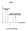
- the present invention aims at offering a quadrature modulation system that is capable of generating a quadrature modulated analog signal wherein the amount of the image signal component (unnecessary signal component) is reduced as compared with conventional technologies, and a transmitter equipped with the quadrature modulation system.
- the invention provides as follows.
- the quadrature modulation system inputs an inphase signal component and an orthogonal signal component, which are provided to a quadrature modulator for outputting a quadrature modulated signal, a part of the quadrature modulated signal serving as a feedback signal, including:
- the amount of the image signal component mixed in the analog signal generated by the quadrature modulation method is reduced.
- Embodiment 1 is to reduce the image signal component mixed in the generated analog signal by adjusting timing relations between the inphase signal component and the orthogonal signal component.
- Embodiment 2 is to obtain the same effects by adjusting the amplitudes of the inphase signal component and the orthogonal signal component.
- Embodiment 3 is to obtain the same effect by adjusting an orthogonality deflection (angular deflection) between the real axis and the imaginary axis.
- Embodiment 4 is to obtain the same effect by collectively adjusting the timing, amplitude, and angular deflection of the inphase signal component and the orthogonal signal component.
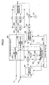
- Fig. 2 is a block diagram of the quadrature modulation system according to Embodiment 1 of the present invention.
- the quadrature modulation system carries out quadrature modulation of an inphase signal component Tx i (I channel) and an orthogonal signal component Tx q (Q channel) of a digital signal that represents contents to be transmitted, and outputs an output signal S that is an analog RF signal.
- the quadrature modulation system includes a compensation circuit 202 serving as an adjustment circuit, digital-to-analog converters 204 and 206, filters 208 and 210, and a quadrature modulator 212.
- the quadrature modulation system includes a multiplying unit 216, a local oscillator 214, an analog-to-digital converter 218, a quadrature demodulator 220, and a phase detector 236, constituting a feedback path.
- the quadrature modulation system includes adders 224 and 226 (in the illustrated example, they function as subtractors), integrators 228 and 230, a time difference detector 232, and a delay circuit 234, these serving as time difference detection means.
- the quadrature modulation system includes a compensation circuit 202 that further includes an I ch compensation unit 237 for the inphase signal component, and a Q ch compensation unit 238 for the orthogonal signal component.
- the digital-to-analog converters 204 and 206 convert the inphase signal component and the orthogonal signal component, respectively, from digital to analog format.
- the filters 208 and 210 are bandpass filters for the respective analog signals.
- the quadrature modulator 212 combines the inphase signal component and the orthogonal signal component that are provided by the respective digital-to-analog converters, and outputs the output signal S.
- y i (n) represents the inphase signal component input into the quadrature modulator 212, which is an amount of the analog signal obtained by D-to-A conversion of the inphase signal component Tx i (n) that is in digital format.
- y q (n) represents the orthogonal signal component input into the quadrature modulator 212, which is an amount of the analog signal obtained by D-to-A conversion of the orthogonal signal component Tx q (n) that is in digital format.
- n represents a parameter that specifies a sample
- ⁇ represents a carrier angular frequency.
- the multiplying unit 216 multiplies the output signal S and a signal provided by the local oscillator 214 such that frequency conversion (down conversion) to low frequency from high frequency is carried out, providing an analog signal at a low frequency.
- the analog-to-digital converter 218 is for converting the analog signal into a digital signal.
- the quadrature demodulator 220 is for demodulating the output of the analog-to-digital converter 218, and outputs an inphase signal component Fb i and an orthogonal signal component Fbq of the feedback signal.
- the adder 224 here functions as a subtractor, and is for obtaining the difference between the inphase signal component Tx i (before quadrature modulation), and the inphase signal component Fb i (of the feedback signal). The difference is totaled by the integrator 228, and a first accumulation value is calculated.
- the adder 226 also functions as a subtractor, and is for obtaining the difference between the orthogonal signal component Tx q (before quadrature modulation), and the orthogonal signal component Fb q (of the feedback signal). The difference is totaled by the integrator 230, and a second accumulation value is calculated.
- the time difference detector 232 obtains a time difference between the inphase signal component and the orthogonal signal component based on the first and the second accumulation values.
- the time difference is mainly generated while the signal components are being processed in the analog format.
- the time difference is mainly generated between the digital-to-analog converter 204 and the quadrature modulator 212, and between the digital-to-analog converter 206 and the quadrature modulator 212.
- a time difference may be generated for the feedback signal due to the analog signal process between the quadrature modulator 212 and the quadrature demodulator 220, the time difference generated in the feedback path is equally introduced to the inphase signal component and the orthogonal signal component. For this reason, the time difference generated in the feedback path does not contribute to the time difference between the inphase signal component and the orthogonal signal component.
- the delay circuit 234 is for adjusting the timing of the signals Tx i and Tx q to be added by the adders 224 and 226, respectively (actually, subtraction takes place), and is additionally capable of setting up a time difference between the digital signals Tx i and Tx q .
- the time difference can be set up by adjusting tap coefficients of a finite impulse response (FIR) filter, for example, the present invention is not limited to this.
- the I ch compensation unit 237 and the Q ch compensation unit 238 in the compensation circuit 202 set up the amount of delay of respective signal components such that the time difference detected by the time difference detector 232 is compensated for.
- the phase detector 236 compares the digital signal inphase component Tx i with the feedback signal inphase component Fb i , both components being input to the adder 224.
- the phase detector 236 compares the digital signal orthogonal component Tx q with the feedback signal orthogonal component Fb q , both components being input to the adder 226. Then, the phase detector 236 determines a phase rotation angle ⁇ between the digital signal and the feedback signal.
- the information about the phase rotation angle ⁇ is provided to the quadrature demodulator 220 such that the phase rotation between the signals before and after the quadrature modulation is compensated for.
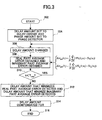
- Fig. 3 is a flowchart for adjusting the amount of the time difference.
- the flow starts at Step 302, and progresses to Step 304.
- the phase rotation angle ⁇ is obtained by the phase detector 236, and the phase rotation angle ⁇ is compensated for by the quadrature demodulator 220.
- an imaginary part error average Err Qch (t) serving as "the second cumulative total” are obtained using the following formula (1).
- n is a parameter for specifying a sample of the digital signal
- N represents the number of times each of the integrators 228 and 230 carries out totaling.
- the adder 224 and the integrator 228 carry out calculation of the real part error average
- the adder 226 and the integrator 230 carry out calculation of the imaginary part error average.
- Step 310 whether the first and second accumulative totals are obtained for all the time delay amounts t is determined. More specifically, whether the time delay t is increased from 0 to a predetermined maximum T max at increments of ⁇ t is determined. If t has not reached the maximum T max , the process returns to Step 306, where t is incremented by ⁇ t, and the same process is performed. In this manner, the amount of time delay t is updated by changing the amount of delay set up by the delay circuit 234.
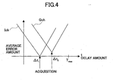
- Step 312 By repeating Steps 306, 308, and 310, relations between the amount of time delay t and the first cumulative total (average error value about the inphase signal component), and between the amount of time delay t and the second cumulative total (average error value about the orthogonal signal component) as shown in Fig. 4 are acquired.
- the two graphs coincide if there is no time difference between the inphase signal component and the orthogonal signal component.
- Step 312 an amount ⁇ t 1 of time delay at which the real part error average becomes the smallest, and an amount ⁇ t 2 of time delay at which the imaginary part error average serve becomes the smallest are obtained by the time difference detector 232.
- suitable delay amounts based on ⁇ t 1 and ⁇ t 2 are provided to the compensation circuit 202 such that the time difference between the inphase signal component and the orthogonal signal component detected at Step 312 is compensated for.
- both amounts of time delay of the inphase and the orthogonal signal components are positively set up. This is because the timings of the inphase and the orthogonal signal components are to relatively agree.
- the amount of time delay equal to ( ⁇ t 1 - ⁇ t 2 )/2 to the I ch compensation unit 237 for the inphase signal component, and to set the amount of delay of ( ⁇ t 2 - ⁇ t 1 )/2 to the Q ch compensation unit 238 for the orthogonal signal component. It is desirable, from viewpoints such as stabilization of control action, to carry out the compensation on both sides.
- Step 316 for ending.
- the present invention is not limited to such a form.
- the time difference can be obtained by calculating a product of the digital signal components Tx i and Tx q and a product of the feedback signal components Fb i and Fbq using the multiplying units 524 and 526, respectively, and by totaling the products (power) with the integrators 228 and 230, respectively.
- Fig. 6 is a flowchart showing a process wherein the products are used as described above.
- the flow starts at Step 602, and progresses to Step 604.
- the phase rotation angle ⁇ is obtained by the phase detector 236, and the phase rotation angle ⁇ is compensated for by the quadrature demodulator 220.
- a real part multiplication average PowIch(t), serving as the first cumulative total, and an imaginary part multiplication average PowQch(t), serving as the second cumulative total are calculated according to the following formula (2).
- n is a parameter for specifying a sample of the digital signal
- N represents the number of times each of the integrators 228 and 230 carries out totaling.
- the multiplying unit 524 and the integrator 228 carry out calculation of the real part multiplication average
- the multiplying unit 526 and the integrator 230 carry out calculation of the imaginary part multiplication average.
- Step 610 whether the first and the second cumulative totals are calculated for all the t values is determined. If t ⁇ T max, the process returns to Step 606, and the same process is performed.
- Step 612 the process progresses to Step 612.
- the time difference detector 232 obtains a delay amount ⁇ t 1 that provides the greatest real part multiplication average, and a delay amount ⁇ t 2 that provides the greatest imaginary part multiplication average.
- Step 614 suitable delay amounts based on ⁇ t 1 and ⁇ t 2 are provided to the compensation circuit 202 such that the time difference between the inphase signal component and the orthogonal signal component detected at Step 612 is compensated for. Then, the process progressed to Step 616 for ending.
- each of the compensation units 237 and 238 of the compensation circuit 202 for adjusting the timing of the inphase signal component and the orthogonal signal component, respectively can be constituted by, for example, a finite impulse response filter (FIR filter).
- FIR filter finite impulse response filter
- a desired amount of time delay can be provided to an input signal for outputting.
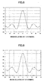
- a time delay equivalent to 1/8 symbol can be provided by adopting values of eight points of the impulse response property of the FIR filter as shown by Fig. 8 as the tap coefficients.
- a time delay equivalent to 5/8 symbol can be obtained by adopting the values of the eight points as shown in Fig. 9 as the tap coefficients.
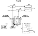
- Fig. 10 is a block diagram showing the variation of the compensation circuit.
- the compensation circuit includes a clock source 1002, a delay element 1004, and selectors 1006 and 1008.
- the clock source 1002 generates a clock signal for driving the digital-to-analog converters 204 (DA 1 ) and 206 (DA 2 ).
- the delay element 1004 delays the timing of the clock signal provided by the clock source 1002 such that delayed clock signals having various delays ⁇ n are output. In the example that is illustrated, five clock signals having delay times ⁇ 0 through ⁇ 4 are prepared.
- Selectors 1006 and 1008 are for selecting one of the clock signals with a delay time ⁇ n based on the delay information provided by the time difference detector 232, and for supplying clock signals with selected time delays to the digital-to-analog converters 204 and 206, respectively.
- Embodiment 2 wherein the image signal component is reduced by adjusting the amplitudes of the inphase signal component and the orthogonal signal component.
- an outline is presented concerning the balance of the amplitudes of the inphase signal component and the orthogonal signal component.
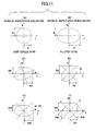
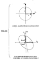
- Fig. 11 shows relations between the amplitudes of the inphase signal component and the orthogonal signal component, and a phase rotation angle where applicable.
- Each of the relations is drawn as a locus when an average of a signal point that is present in a minute unit angle on a signal point arrangement plan (constellation) is calculated for 0 through 360 degrees.
- a circular locus is obtained as shown at (A) of Fig. 11.
- an elliptic locus is obtained as shown at (B) of Fig. 11.
- the amplitude of the inphase signal component and/or the orthogonal signal component is adjusted such that the elliptic locus turn into a circular locus, namely, such that the amplitude ratio of the real axis to the imaginary axis become 1, that is, the amplitude difference become zero.
- phase rotation angle phase rotation angle
- the amplitude balance can be obtained by adjusting the amplitudes of the inphase signal component and the orthogonal signal component.
- the phase rotation angle ⁇ becomes as great as 45 degrees ( ⁇ /4 rad.) as shown at (D) of Fig.
- an average amplitude A0 in the real axis (I) and an average amplitude B0 in the imaginary axis (Q) become equal, even if the locus is in the elliptic shape. That is, when the phase rotation angle ⁇ is about 45 degrees, the amplitude difference cannot be properly detected, and it is difficult to compensate for the imbalance of the amplitudes.
- average amplitudes A45 and B45 are measured.
- A45 and B45 are amplitude values when the feedback signal is rotated by 45 degrees in the direction of the arrow (i.e., -45 degrees) as shown at (E) of Fig. 11. In this manner, two pairs of the inphase signal component and the orthogonal signal component are obtained.
- one is the pair of the average amplitude values A0 and B0 measured without rotating the feedback signal, and the other is the pair of the average amplitude values A45 and B45 measured when the feedback signal is rotated by 45 degrees, as shown at (F) of Fig. 11.
- the present embodiment is to obtain the amplitude balance based on the two pairs.
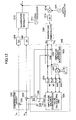
- Fig. 12 is a block diagram of the quadrature modulation system according to the embodiment of the present invention.
- the quadrature modulation system includes a compensation circuit 1202, digital-to-analog converters 1204 and 1206, a quadrature modulator 1212, and a local oscillator 1211.
- the quadrature modulation system includes a multiplying unit 1216 connected to another local oscillator 1214, an analog-to-digital converter 1218, and a quadrature demodulator 1220 in the feedback path.
- the quadrature modulation system includes an amplitude difference calculating unit 1240 that includes an amplitude balance detecting unit 1222, averaging units (Ave) 1224, a compound multiplier 1225, an amplitude balance compensation value calculating unit 1226, and switches 1228 and 1230.
- the compensation circuit 1202 includes multiplying units 1232 and 1234.
- the amplitude balance detecting unit 1222 includes multiplying units 1236 and 1238.
- the digital-to-analog converters 1204 and 1206 convert the inphase signal component and the orthogonal signal component, respectively, from digital format to analog format.
- the quadrature modulator 1212 receives and combines the inphase signal component and the orthogonal signal component, and outputs the output signal S.
- the multiplying unit 1216 is for multiplying the output signal S and a signal from the local oscillator 1214, wherein down conversion is carried out.
- the analog-to-digital converter 1218 converts the down-converted signal, which is an analog signal, into a digital signal.
- the quadrature demodulator 1220 carries out the quadrature demodulation of the output from the analog-to-digital converter 1218, and outputs an inphase signal component Fb i and an orthogonal signal component Fb q of the feedback signal.
- the multiplying units 1236 and 1238 of the amplitude balance detecting unit 1222 provisionally adjust the amplitudes of the inphase signal component Fb i and the orthogonal signal component Fb q , respectively, of the feedback signal, and output Fb i and Fb q to the averaging units 1224 and the compound multiplier 1225.
- the compound multiplier 1225 rotates the phase of the output feedback signal by 45 degrees, and outputs the rotated feedback signal.
- the averaging units 1224 calculate averages of the respective signals that are input. Namely, according to this example, the averages A0 and B0 of the amplitudes measured without rotating the feedback signal, and the averages A45 and B45 of the amplitudes measured with rotating the feedback signal by 45 degrees are calculated.
- the amplitude balance compensation value calculating unit 1226 calculates amplitude balance compensation values Ci and Cq based on the averages obtained by the averaging units 1224. Eventually (see below), the amplitude balance compensation values Ci and Cq are multiplied by the digital signals Tx i and Tx q , respectively.
- the switches 1228 and 1230 are turned to a side indicated by “1" (side “1") until the amplitude balance compensation values Ci and Cq converge, and the outputs from the amplitude balance compensation value calculating unit 1226 are directed to the side "1".
- the outputs from the amplitude balance compensation value calculating unit 1226 are directed to the side indicated by "0" (side “0").
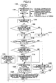
- Fig. 13 is a flowchart for adjusting the amplitude balance.
- the process starts at Step 1302 and progresses to Step 1304.
- various parameters such as a previous error amount PreErr, a direction d of compensation, a step size ⁇ , and a threshold value for error Err_th are initialized.
- the amplitude balance compensation values Ci and Cq for the inphase signal component and the orthogonal signal component, respectively, are set at 1.
- a great value is set to the previous error amount PreErr.
- the compensation direction d is set as +1. According to the present embodiment, if the compensation direction d is +1, Cq is increased while Ci is reduced; and if d is set as -1, Cq is reduced while Ci is increased.
- the average amplitude A0 of the inphase signal component and the average amplitude B0 of the orthogonal signal component of the feedback signal are measured without carrying out phase rotation, and an absolute value of the difference between A0 and B0 is obtained, which is called Err0.
- Err0 Abs(A0-B0)
- the average amplitude A45 of the inphase signal component and the average amplitude B45 of the orthogonal signal component are measured with the phase of the feedback signal being rotated by 45 degrees, and an absolute value of the difference between A45 and B45 is obtained, which is called Err45.
- Err45 Abs(A45-B45)
- Step 1308 the absolute values of Err0 and Err45 are compared, and the greater of the two (or Err45 if they are equal) is assigned as the value of an error Err, which is evaluated in operations afterwards, namely, at Steps 1310 and 1312.
- Step 1314 determines whether the error Err is greater than the threshold Err_th. If the determination is affirmative, the process progresses to Step 1316.
- Step 1316 determines whether the error Err is greater than or equal to the previous error amount PreErr. If the determination is affirmative, the process progresses to Step 1318, where the value of the compensation direction d is changed; otherwise, the process progresses to Step 1320.
- the amplitude balance compensation values Ci and Cq are updated.
- the amplitude balance compensation values Ci and Cq are updated such that the difference between Ci and Cq is changed by an amount equal to ⁇ . Err.
- the parameter ⁇ represents the step size for updating the compensation values.
- updating is performed not by changing only one of Ci and Cq with the other being fixed, but rather by changing both Ci and Cq by the same amount in opposite directions. In this manner, the updating operation can be carried out, with the control action being stabilized.
- the updated amplitude balance compensation values Ci and Cq are provided to the amplitude balance detecting unit 1222.
- Step 1324 the previous error amount PreErr is assigned the value Err, the process returns to Step 1306, and the same operation as described above follows.
- Step 1314 if the error Err is determined to be less than or equal to the threshold Err_th, the process progresses to Step 1326.
- Step 1326 the switches 1228 and 1230 are turned to the side "0" such that the outputs from the amplitude balance compensation value calculating unit 1226 are directed to the compensation circuit 1202. Accordingly, the optimal amplitude balance compensation values Ci and Cq are provided to the multiplying units 1232 and 1234, respectively, of the compensation circuit 1202. Then, the process progresses to Step 1328 for ending. In this manner, the amplitude balance is adjusted.
- Fig. 14 is a conceptual diagram for explaining another embodiment of the present invention.
- Fig. 14 shows relations between the orthogonality of the inphase signal component and the orthogonal signal component, and the average amplitude vector for every quadrant.
- a modulation technique like QPSK is assumed in this embodiment, naturally the embodiment is applicable to other modulation techniques.
- average amplitude vectors r1, r2, r3, and r4 are calculated for the corresponding quadrants.
- average amplitude vectors taken from minute unit angles draw a circular locus on a signal point arrangement plan, i.e., a constellation chart, as shown at (A) of Fig. 14.
- the magnitude of the four average amplitude vectors r1, r2, r3, and r4 are equal to each other, and r1 and r2 are orthogonal, r1 and r4 are orthogonal; similarly, r3 and r2 are orthogonal, and r3 and r4 are orthogonal.
- the following cases can be considered.
- the first of the cases is as shown at (B) of Fig. 14, wherein not all the magnitudes of the average amplitude vectors are the same, and the average amplitude vectors are not orthogonal.
- the second of the cases is as shown at (C) of Fig. 14, wherein not all the magnitudes of the average amplitude vectors are the same, although the average amplitude vectors are orthogonal to each other.
- the third case is as shown at (D) of Fig. 14, wherein although all the average amplitude vectors are of the same magnitude, they are not orthogonal.
- the present embodiment uses the relations between the average amplitude vectors for compensating for the imbalance of the amplitudes.
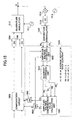
- Fig. 15 is a block diagram of the quadrature modulation system according to the present embodiment.
- the quadrature modulation system includes a compensation circuit 1502, digital-to-analog converters 1504 and 1506, and a quadrature modulator 1512 connected to a local oscillator 1511.
- the quadrature modulation system includes a multiplying unit 1516 connected to the local oscillator 1514, an analog-to-digital converter 1518, and a quadrature demodulator 1520 in the feedback path.
- the quadrature modulation system includes an amplitude difference calculating unit 1540 that further includes an amplitude balance detecting unit 1522, an quadrant averaging unit 1524, an amplitude balance compensation value calculating unit 1526, and switches 1528 and 1530.
- the digital-to-analog converters 1504 and 1506 convert the inphase signal component and the orthogonal signal component, respectively, from digital to analog format.
- the quadrature modulator 1512 combines the inphase signal component and the orthogonal signal component that are provided by the respective digital-to-analog converters, and outputs the output signal S.
- the multiplying unit 1516 multiplies the output signal S and the signal from the local oscillator 1514, wherein down conversion is carried out.
- the analog-to-digital converter 1518 converts the down-converted signal, which is an analog signal, into a digital signal.
- the quadrature demodulator 1520 carries out the quadrature demodulation of the output of the analog-to-digital converter 1518, and outputs the inphase signal component Fb i and the orthogonal signal component Fbq of the feedback signal.
- the amplitude balance detecting unit 1522 provisionally adjusts the inphase signal component Fb i and the orthogonal signal component Fbq of the feedback signal, and outputs Fb i and Fbq to the quadrant averaging unit 1524.
- R1 is equivalent to an average vector in one of main axis directions of the ellipse
- R2 is equivalent to an average vector in the other of the main axis directions of the ellipse. If the proper balance of the amplitudes is present,
- the amplitude balance compensation value calculating unit 1526 calculates the amplitude balance compensation values Ci and Cq based on the averages obtained by the quadrant averaging unit 1524. Eventually the amplitude balance compensation values Ci and Cq are provided to the compensation circuit 1502, serving as the coefficients with which the digital signals Txi and Txq, respectively, are multiplied.
- the switches 1528 and 1530 are turned to the side of "1" until the amplitude balance compensation values Ci and Cq converge such that the outputs from the amplitude balance compensation value calculating unit 1526 are directed to the compensation circuit 1502. When the amplitude balance compensation values Ci and Cq converge, the switches 1528 and 1530 are turned to the side "0".
- Fig. 16 is a flowchart for adjusting the amplitude balance. The process starts at 1602 and progresses to Step 1604.
- various parameters such as amplitude balance compensation values Ci and Cq, a switch position SW, a step size ⁇ , a previous amplitude error value PreErrAmp, and a threshold value for average amplitude error Err_th are initialized.
- the amplitude balance compensation values Ci and Cq for the inphase signal component and the orthogonal signal component, respectively are set at 1.
- a great value is set to the previous amplitude error value PreErrAmp and the previous phase error value PreErrPh.
- the compensation direction d is set as +1, in which case, Ci is increased while Cq is reduced. When d is set as -1, Ci is reduced while Cq is increased.
- Step 1614 whether the amplitude error ErrAmp is greater than a predetermined threshold ErrAmp_th is determined. If the determination is affirmative, the process progresses to Step 1616.
- Step 1616 whether the amplitude error ErrAmp is greater than or equal to the last error PreErrAmp is determined. If the determination is affirmative, the process progresses to Step 1618, where the value of the compensation direction d is changed, and the process progresses to Step 1620. If the determination at Step 1616 is negative, the process progresses to Step 1620.
- the amplitude balance compensation values Ci and Cq are updated.
- the amplitude balance compensation values Ci and Cq are updated such that the difference between Ci and Cq is changed by an amount equal to ⁇ ⁇ ErrAmp.
- the updated amplitude balance compensation values Ci and Cq are set to the amplitude balance detecting unit 1522.
- the amplitude error ErrAmp is set as the value of the previous amplitude error PreErrAmp, and the process returns to Step 1606. Henceforth, the same operation as described above follows.
- Step 1614 if the amplitude error ErrAmp is determined to be less than or equal to the predetermined threshold ErrAmp_th, the process progresses to Step 1632.
- R1 i represents an inphase component
- R1 q represents an orthogonal component of the vector along one of the main axes of the ellipse. In the case such as shown at (D) of Fig. 14, the process comes to Step 1632.
- Step 1634 whether the phase error ErrPh is greater than a predetermined threshold ErrPh_th is determined. If the determination is affirmative, the process progresses to Step 1636.
- Step 1636 whether the phase error ErrPh is greater than or equal to the previous error PreErrPh is determined. If the determination is affirmative, the process progresses to Step 1638, where the value of the compensation direction d is changed, and the process progresses to Step 1640. If the determination at Step 1636 is negative, the process progresses directly to Step 1640.
- the amplitude balance compensation values Ci and Cq are updated.
- the amplitude balance compensation values Ci and Cq are updated such that the difference between Ci and Cq become greater by an amount equal to ⁇ ⁇ ErrPh.
- the updated amplitude balance compensation values Ci and Cq are set to the amplitude balance detecting unit 1522.
- the phase error ErrPh is set as the value of the previous phase error PreErrPh.
- the process returns to Step 1606, and henceforth the same operation as described above follows.
- Step 1634 if the phase error ErrPh is determined to be less than or equal to the predetermined threshold ErrPh_th, the process progresses to Step 1646.
- Step 1646 the switches 1528 and 1530 are turned to the side "0" such that the outputs of the amplitude balance compensation value calculating unit 1526 are provided to the compensation circuit 1502. Then, the process progresses to Step 1648, where the process for adjusting the amplitude balance ends.
- Fig. 17 is a block diagram of the quadrature modulation system according to another embodiment of the present invention.
- the quadrature modulation system includes a compensation circuit 1702, digital-to-analog converters 1704 and 1706, and a quadrature modulator 1712 connected to a local oscillator 1711.
- the quadrature modulation system includes a multiplying unit 1716 connected to the local oscillator 1714, an analog-to-digital converter 1718, and a quadrature demodulator 1720 in the feedback path.
- the quadrature modulation system includes an amplitude difference calculating unit 1740 that further includes an amplitude balance detecting unit 1722, an amplitude balance compensation value calculating unit 1726, and switches 1728 and 1730.
- the quadrature modulation system includes a phase detector 1732.
- the digital-to-analog converters 1704 and 1706 convert the inphase signal component and the orthogonal signal component, respectively, from digital to analog format.
- the quadrature modulator 1712 combines the inphase signal component and the orthogonal signal component that are provided by the respective digital-to-analog converters, and outputs the output signal S.
- the multiplying unit 1716 multiplies the output signal S and a signal from the local oscillator 1714, wherein down conversion is carried out.
- the analog-to-digital converter 1718 converts the down-converted signal, which is an analog signal, into a digital signal.
- the quadrature demodulator 1720 carries out the quadrature demodulation of the output of the analog-to-digital converter 1718, and outputs the inphase signal component Fb i and the orthogonal signal component Fbq of the feedback signal.
- the amplitude balance detecting unit 1722 provisionally adjusts the amplitudes of the inphase signal component Fb i and the orthogonal signal component Fbq of the feedback signal, and outputs Fb i and Fbq to the amplitude balance compensation value calculating unit 1726.
- the amplitude balance compensation value calculating unit 1726 calculates the amplitude balance compensation values Ci and Cq based on the output from the amplitude balance detecting unit 1722.
- the switches 1728 and 1730 are turned to the side "1" until the amplitude balance compensation values Ci and Cq converge such that the outputs from the amplitude balance compensation value calculating unit 1726 are provided to the amplitude balance detecting unit 1722.
- the switches 1728 and 1730 are turned to the side "0" such that the outputs from the amplitude balance compensation value calculating unit 1726 are provided to the compensation circuit 1702.
- the phase detector 1732 compares the digital signal components Tx i and Tx q with the feedback signal components Fb i and Fb q , respectively, and obtains the phase rotation angle ⁇ between the digital signal and the feedback signal.
- the information about the phase rotation angle ⁇ is provided to the quadrature demodulator 1720 such that the phase rotation between both signals is compensated for.
- Fig. 18 is a flowchart for adjusting the amplitude balance. The process starts at 1802 and progresses to Step 1804. At Step 1804, various parameters such as a switch position SW, a step size ⁇ , and a threshold value for average amplitude error Err_th are initialized. In the present example, the amplitude balance compensation values Ci and Cq for the inphase signal component and the orthogonal signal component, respectively, are set at 1.
- Step 1806 the average amplitude of the inphase signal component Tx i and the orthogonal signal component Tx q before quadrature modulation are measured, serving as A ref and B ref , respectively.
- the average amplitude of the inphase signal component Fb i and the orthogonal signal component Fbq of the feedback signal are measured, serving as A fb and B fb , respectively.
- the average amplitude errors ErrA and ErrB are normalized based on the amplitude values A ref and B ref , respectively.
- the normalized values are called ErrA_norm and ErrB_norm, respectively.
- Step 1814 whether the absolute value of the normalized amplitude error ErrA norm is greater than a predetermined threshold Err_th is determined. Further, whether the absolute value of the normalized amplitude error ErrB_norm is greater than the predetermined threshold Err_th is determined. If at least one of the absolute values of the normalized amplitude error is determined to be greater than the threshold, the process progresses to Step 1816.
- the amplitude balance compensation values Ci and Cq are updated.
- the amplitude balance compensation value Ci for the inphase signal component is changed by an amount equal to ⁇ ⁇ ErrA_norm
- the amplitude balance compensation value Cq for the orthogonal signal component is changed by an amount equal to ⁇ ⁇ ErrB.
- Step 1818 the updated amplitude balance compensation values Ci and Cq are set to the amplitude balance detecting unit 1722, and the process returns to Step 1806. Henceforth, the same operation as described above follows.
- Step 1814 if the normalized amplitude error is determined to be less than or equal to the predetermined threshold Err_th, the process progresses to Step 1820.
- Step 1820 the switches 1728 and 1730 are turned to the side "0" such that the outputs of the amplitude balance compensation value calculating unit 1726 are provided to the compensation circuit 1702. Then, the process progresses to Step 1822 for ending the amplitude balance adjustment.
- Fig. 19 is a block diagram of the quadrature modulation system according to another embodiment of the present invention.
- the quadrature modulation system includes a compensation circuit 1902, digital-to-analog converters 1904 and 1906, and a quadrature modulator 1912 connected to a local oscillator 1911.
- the quadrature modulation system includes a multiplying unit 1916 connected to the local oscillator 1914, an analog-to-digital converter 1918, and a quadrature demodulator 1920.
- the quadrature modulation system includes an amplitude difference calculating unit 1940 that includes an amplitude balance detecting unit 1922, an amplitude balance compensation value calculating unit 1926, switches 1928 and 1930, multiplying units 1932 and 1934, and averaging units (Ave) 1936 and 1938.
- the digital-to-analog converters 1904 and 1906 convert the inphase signal component and the orthogonal signal component, respectively, from digital to analog format.
- the quadrature modulator 1912 combines the inphase signal component and the orthogonal signal component that are provided by the respective digital-to-analog converters, and outputs the output signal S.
- the multiplying unit 1916 multiplies the output signal S and a signal from the local oscillator 1914, wherein down conversion is carried out.
- the analog-to-digital converter 1918 converts the down-converted signal, which is an analog signal, into a digital signal.
- the quadrature demodulator 1920 carries out the quadrature demodulation of the output of the analog-to-digital converter 1918, and outputs the inphase signal component Fb i and the orthogonal signal component Fbq of the feedback signal.
- the amplitude balance detecting unit 1922 provisionally adjusts the amplitudes of the inphase signal component Fb i and the orthogonal signal component Fb q of the feedback signal, and outputs the signal components Fb i and Fb q to the amplitude balance compensation value calculating unit 1926.
- the amplitude balance compensation value calculating unit 1926 calculates the amplitude balance compensation values Ci and Cq based on the outputs from the amplitude balance detecting unit 1922.
- the switches 1928 and 1930 are turned to the side "1" until the amplitude balance compensation values Ci and Cq converge such that the outputs from the amplitude balance compensation value calculating unit 1926 are provided to the amplitude balance detecting unit 1922.
- the switches 1928 and 1930 are turned to the side "0" such that the outputs from the amplitude balance compensation value calculating unit 1926 are provided to the compensation circuit 1902.
- the multiplying unit 1932 multiplies the inphase signal component Tx i before quadrature modulation as a reference signal Ref i , and the orthogonal signal component Fbq of the feedback signal.
- the product is equalized by the averaging unit 1936, and is output as a first average Ave1.
- the multiplying unit 1934 multiplies the orthogonal signal component Tx q before quadrature modulation as a reference signal Refq, and the inphase signal component Fb i of the feedback signal.
- the product is equalized by the averaging unit 1938, and is output as a second average Ave2.
- the inphase component Fb i and the orthogonal component Fbq of a demodulated signal Fb in the baseband band obtained from the feedback signal are expressed by the following formula, where ⁇ represents the phase rotation of the feedback signal.
- Fb i A ⁇ Ref i - ⁇ cos ⁇ + B ⁇ Ref q ⁇ sin ⁇
- Fb q A ⁇ Ref i ⁇ sin ⁇ - B ⁇ Ref q ⁇ cos ⁇
- E[] is an expression of equalization, and is obtained by dividing a value totaled by the integrator by a suitable factor.
- the ratio provides a measure of the amplitude balance. If the ratio is close to 1, the amplitude balance is proper, and as the ratio departs from 1, amplitude imbalance increases. In the present embodiment, the ratio is calculated, and the amplitudes of the inphase signal component and the orthogonal signal component are adjusted such that the ratio approach 1.
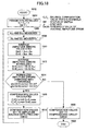
- Fig. 20 is a flowchart for adjusting the amplitude balance.
- the process starts at Step 2002, and progresses to Step 2004.
- various parameters such as a previous balance error amount PreErr, a direction d of compensation, a step size ⁇ , and a threshold value for the balance error Err_th are initialized.
- the amplitude balance compensation values Ci and Cq of the inphase signal component and the orthogonal signal component, respectively are set at 1.
- a great value is set to the previous error PreErr.
- the compensation direction d which can take one of the values +1 and -1, is set at +1.
- the first average Ave1 and the second average Ave2 are calculated.
- Step 2008 the inphase average power P ref_i and the orthogonal average power P ref_q before the quadrature modulation are measured.
- Step 2014 whether the error Err is greater than a predetermined threshold Err_th is determined. If the determination is affirmative, the process progresses to Step 2016.
- Step 2016, whether the error Err is greater than or equal to the previous error PreErr is determined. If the determination is affirmative, the process progresses to Step 2018, where the value of the compensation direction d is changed, and the process progresses to Step 2020. If the determination at Step 2016 is negative, the process progresses directly to Step 2020.
- the amplitude balance compensation values Ci and Cq are updated.
- the amplitude balance compensation values Ci and Cq are updated such that the difference between Ci and Cq is made greater by an amount equal to ⁇ ⁇ Err.
- the updated amplitude balance compensation values Ci and Cq are set to the amplitude balance detecting unit 1922.
- the error Err is set as the value of the previous error PreErr, and the process returns to Step 2006. Henceforth, the same operation as described above follows.
- Step 2014 if the error Err is determined to be less than or equal to the predetermined threshold Err_th, the process progresses to Step 2026.
- Step 2026 the switches 1928 and 1930 are turned to the side "0" such that the outputs of the amplitude balance compensation value calculating unit 1926 are provided to the compensation circuit 1902. Then, the process progresses to Step 2028 for completing the amplitude balance adjustment.
- the amplitude balance compensation values Ci and Cq may be provided to the digital signals as shown by Fig. 12, or alternatively, to the analog signals as shown in Fig. 21.
- Embodiment 3 wherein the image signal component is reduced by adjusting a deviance of the orthogonality relation between the real axis and the imaginary axis (angle deflection or orthogonality deflection).
- angle deflection or orthogonality deflection a deviance of the orthogonality relation between the real axis and the imaginary axis
- a locus of the averages of the signal points that are present in minute unit angles of 0 - 360 degrees is shown, which represents the case wherein the inphase signal component and the orthogonal signal component are properly output.
- the real axis and the imaginary axis are in orthogonal relation.
- the real axis Re and the imaginary axis Im cross at an angle different from 90 degrees by ⁇ .
- the inphase signal component I and the orthogonal signal component Q are distorted, and are respectively expressed by the following formulas.
- phase rotation angle ⁇ discussed in reference to Figs. 2, 5, 11, 14, and 17 refers to the phase rotation around the origin of the feedback signal with the real axis and the imaginary axis being kept at 90 degrees.
- Fig. 23 is a block diagram of the quadrature modulation system according to Embodiment 3.
- the quadrature modulation system includes an orthogonality deflection compensation circuit 2302, digital-to-analog converters 2304 and 2306, and a quadrature modulator 2312 connected to a local oscillator 2311.
- the quadrature modulation system includes a multiplying unit 2316 connected to the local oscillator 2314, an analog-to-digital converter 2318, and a quadrature demodulator 2320.
- the quadrature modulation system includes an angle deflection calculating unit 2336 that includes an orthogonality deflection detecting unit 2322, absolute value accumulating units 2324 and 2326, and an difference amount determining unit 2328.
- the digital-to-analog converters 2304 and 2306 convert the inphase signal component and the orthogonal signal component, respectively, of a digital format into analog format.
- the quadrature modulator 2312 combines the inphase signal component and the orthogonal signal component that are provided by the respective digital-to-analog converters, and outputs the output signal S.
- the multiplying unit 2316 multiplies the output signal S and a signal from the local oscillator 2314, wherein down conversion is carried out.
- the analog-to-digital converter 2318 converts the down-converted signal, which is an analog signal, into a digital signal.
- the quadrature demodulator 2320 carries out the quadrature demodulation of the output of an analog-to-digital converter 2318, and outputs the inphase signal component Fb i and the orthogonal signal component Fb q of the feedback signal.
- the orthogonality deflection detecting unit 2322 provisionally adjusts the angle deflection of the inphase signal component Fb i and the orthogonal signal component Fbq of the feedback signal components, and outputs the signal components to the absolute value accumulating unit 2324 and 2326, respectively.
- the absolute value accumulating unit 2324 takes in and totals the absolute value of the inphase signal component Fb i of the feedback signal, and outputs the total as a first cumulative total. Further, the absolute value accumulating unit 2326 takes in and totals the absolute value of the orthogonal signal component Fbq of the feedback signal, and outputs the total as a second cumulative total.
- the difference amount determining unit 2328 calculates an orthogonality deflection ⁇ fb based on the first and second cumulative totals obtained from the absolute value accumulating units 2324 and 2326. Eventually, the orthogonality deflection ⁇ fb becomes the orthogonality deflection ⁇ , which is provided to the orthogonality deflection compensation circuit 2302.
- Fig. 24 is a block diagram showing an example of the orthogonality deflection compensation circuit 2302.
- the orthogonality deflection compensation circuit 2302 includes an adder 2402, multiplying units 2404 and 2406, and coefficient multiplying units 2408 and 2410.
- the adder 2402 outputs a sum of the inphase signal component Tx i and the output of the multiplying unit 2404.
- the multiplying unit 2404 outputs a product of the orthogonal signal component Tx q and the output of the coefficient multiplying unit 2408.
- the multiplying unit 2406 outputs a product of the orthogonal signal component Tx q and the output of the coefficient multiplying unit 2410.
- the coefficient multiplying unit 2408 outputs tan ⁇ based on the angle deflection ⁇ which is the output from the difference amount determining unit 2328.
- the coefficient multiplying unit 2410 outputs 1/cos ⁇ based on the angle deflection ⁇ , which is the output from the difference amount determining unit 2328.
- the output of the adder 2402 is equal to Tx i +Tx q - tan ⁇ , which is provided to the digital-to-analog converter 2304.
- the output of the multiplying unit 2406 is equal to Tx q /cos ⁇ , which is provided to the digital-to-analog converter 2306.
- the real axis is fixed, and the imaginary axis is considered to be in error by ⁇ in describing the present embodiment with reference to Fig. 22, the present invention is not limited to this, but a variation wherein the real axis is deflected is possible.
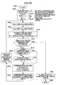
- Fig. 25 is a flowchart for adjusting the angle deflection between the real axis and the imaginary axis.
- the process starts at Step 2502 and progresses to Step 2504.
- various parameters are initialized. Namely, the compensation angle ⁇ fb for the orthogonality deflection detecting unit 2322, and the compensation angle ⁇ for the orthogonality deflection compensation circuit 2302 are set at zero.
- a parameter N for determining convergence is set at zero. Further, an amount of change ⁇ when updating the compensation angle is set at a suitable value.
- Step 2506 a cumulative total of the absolute value of the real part Fb i of the feedback signal is calculated as the first accumulation value.
- Step 2508 a cumulative total of the absolute value of the imaginary part Fbq of the feedback signal is calculated as the second accumulation value.
- an absolute value of the difference between the first cumulative total and the second cumulative total is calculated as an error DiffAcm1.
- Step 2512 whether the error DiffAcm1 is less than or equal to a previous error DiffAcm2 is determined. If the determination is affirmative, the process progresses to Step 2518. Otherwise, the process progresses to Step 2514.
- Step 2514 the direction (the sign) of the compensation angle ⁇ fb to be provided to the orthogonality deflection detecting unit 2322 is reversed.
- the value of the parameter N is incremented by 1.
- the compensation angle ⁇ fb is updated.
- the error DiffAcm1 is set to be the value of the previous error DiffAcm2.
- Step 2522 whether the parameter N is greater than a predetermined value is determined. If the determination is negative, the process returns to Steps 2506 and 2508, and the same process is repeated. If the determination is affirmative, that is, the parameter N is greater than the predetermined value, the process progresses to Step 2524.
- the compensation angle ⁇ fb provided to the orthogonality deflection detecting unit 2322 is provided as the value of the compensation angle ⁇ to the orthogonality deflection compensation circuit 2302.
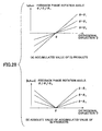
- Fig. 26 shows typical relations between the absolute value of the error DiffAcm1 and the number of times N of updating the compensation value.
- the absolute value of the error almost converges to a value
- the magnitude relations between the absolute value of the error and the value of the previous error frequently change. Accordingly, it is possible to assume that the absolute value of the error is approaching a convergence value by monitoring the value of the parameter N.
- Fig. 27 is a block diagram of the quadrature modulation system according to another embodiment of the present invention.
- the quadrature modulation system includes an orthogonality deflection compensation circuit 2702, digital-to-analog converters 2704 and 2706, and a quadrature modulator 2712 connected to a local oscillator 2711.
- the quadrature modulation system includes a multiplying unit 2716 connected to a local oscillator 2714, an analog-to-digital converter 2718, and a quadrature demodulator 2720.
- the quadrature modulation system includes an angle deflection calculating unit 2736 that includes an orthogonality deflection detecting unit 2722, a multiplying unit 2724, an accumulating unit 2726, and a sign determining unit 2728.
- the digital-to-analog converters 2704 and 2706 convert the inphase signal component and the orthogonal signal component, respectively, from digital to analog format.
- the quadrature modulator 2712 combines the inphase signal component and the orthogonal signal component that are provided by the respective digital-to-analog converters, and outputs the output signal S.
- the multiplying unit 2716 multiplies the output signal S and a signal from the local oscillator 2714, wherein down conversion is carried out.
- the analog-to-digital converter 2718 converts the down-converted signal, which is an analog signal, to a digital signal.
- the quadrature demodulator 2720 carries out the orthogonal demodulation of the output of the analog-to-digital converter 2718, and outputs the inphase signal component Fb i and the orthogonal signal component Fbq of the feedback signal.
- the orthogonality deflection detecting unit 2722 provisionally adjusts the angle deflection of the inphase signal component Fb i and the orthogonal signal component Fb q of the feedback signal, and provides Fb i and Fb q to the multiplying unit 2724.
- the multiplying unit 2724 calculates a product of the inphase signal component Fb i and the orthogonal signal component Fbq of the feedback signal.
- the accumulating unit 2726 totals the output products of the multiplying unit 2724.
- the sign determining unit 2728 calculates orthogonality deflection ⁇ fb based on the accumulative total of the product of the inphase signal component Fb i and the orthogonal signal component Fb q . Eventually, the orthogonality deflection ⁇ fb becomes the orthogonality deflection ⁇ to be provided to the orthogonality deflection compensation circuit 2702.
- a demodulated baseband signal Fb is obtained from the feedback signal, and is expressed by the following formula.
- Fb i Tx i ⁇ cos ⁇ + Tx q ⁇ sin ( ⁇ - ⁇ )
- Fb q Tx i ⁇ sin ⁇ - Tx q ⁇ cos ( ⁇ - ⁇ )
- ⁇ represents the orthogonality deflection between the real axis and the imaginary axis
- ⁇ represents the phase rotation angle of the feedback signal.
- the product of the inphase signal component Fb i of a feedback signal and the orthogonal signal component Fb q is expressed by the following formula.
- Fb i ⁇ Fb q Tx i ⁇ Tx q ⁇ cos (2 ⁇ - ⁇ ) + (1/2)Tx i 2 ⁇ sin 2 ⁇ + (1/2)Tx q 2 ⁇ sin (2 ⁇ -2 ⁇ )
- the second term, (1/2)Tx i 2 ⁇ sin 2 ⁇ , is independent of the orthogonality deflection ⁇ . Therefore, only the third term, (1/2) Tx q 2 ⁇ sin(2 ⁇ -2 ⁇ ), is dependent on the orthogonality deflection ⁇ .
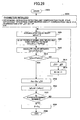
- Fig. 29 is a flowchart for adjusting the angle deflection between the real axis and the imaginary axis. The process starts at Step 2902 and progresses to Step 2904. At Step 2904, various parameters are initialized.
- Step 2908 the cumulative total IqAcm1 of the product of the real part Fb i and the imaginary part Fbq of the feedback signal is calculated.
- the cumulative total is changed into an absolute value.
- this step is dispensable, it is desirable to provide this step for the following reason. Namely, if the conversion into the absolute value is not performed, the optimal compensation angle is determined only by one criterion that is to obtain a compensation angle that provides the null point of the cumulative total as shown at (A) of Fig. 28.
- the absolute value of the cumulative total is prepared as shown at (B) of Fig. 28, another criterion is available, namely, a point where the change rate of the cumulative total changes can be determined to provide the optimal compensation angle.
- the change rate changes before and behind the compensation angle ⁇ , because the sign of the slope changes. For this reason, according to the latter method, the precision in determining the optimal compensation angle is raised.
- Step 2912 whether IqAcm1, which represents the latest and current cumulative total, is less than or equal to IqAcm2, which represents the previous cumulative total, is determined. If the determination is affirmative, the process progresses to Step 2918. Otherwise, the process progresses to Step 2914.
- Step 2914 the direction (the sign) of the compensation angle ⁇ fb to be provided to the orthogonality deflection detecting unit 2722 is reversed.
- Step 2916 the value of the parameter N is incremented by 1.
- Step 2918 the compensation angle ⁇ fb is updated.
- the latest and current cumulative total IqAcm1 is set as the value of the previous accumulative total IqAcm2.
- Step 2922 whether the parameter N is greater than a predetermined value is determined. If the determination is negative, the process returns to Step 2906 for repeating the same process. If the determination is affirmative, the process progresses to Step 2924.
- the compensation angle ⁇ to be provided to the orthogonality deflection compensation circuit 2902 is set at the compensation angle ⁇ fb provided to the orthogonality deflection detecting unit 2922.
- Fig. 30 is a block diagram of the quadrature modulation system according to another embodiment of the present invention.
- the quadrature modulation system includes an orthogonality deflection compensation circuit 3002, digital-to-analog converters 3004 and 3006, and a quadrature modulator 3012 connected to a local oscillator 3011.
- the quadrature modulation system includes a multiplying unit 3016 connected to a local oscillator 3014, an analog-to-digital converter 3018, and a quadrature demodulator 3020.
- the quadrature modulation system includes an angle deflection calculating unit 3036 that includes an orthogonality deflection detecting unit 3022, a fast-Fourier-transform (FFT) processing unit 3024, a power analyzing unit 3026, an orthogonality deflection compensation value calculation unit 3028, and a switch 3030.
- an angle deflection calculating unit 3036 that includes an orthogonality deflection detecting unit 3022, a fast-Fourier-transform (FFT) processing unit 3024, a power analyzing unit 3026, an orthogonality deflection compensation value calculation unit 3028, and a switch 3030.
- FFT fast-Fourier-transform
- the digital-to-analog converters 3004 and 3006 convert the inphase signal component and the orthogonal signal component, respectively, from digital to analog format.
- the quadrature modulator 3012 combines the inphase signal component and the orthogonal signal component that are provided by the respective digital-to-analog converters, and outputs the output signal S.
- the multiplying unit 3016 multiplies the output signal S and a signal from the local oscillator 3014, wherein down conversion is carried out.
- the analog-to-digital converter 3018 converts the down-converted signal, which is an analog signal, into a digital signal.
- the quadrature demodulator 3020 carries out the quadrature demodulation of the output of the analog-to-digital converter 3018, and outputs the inphase signal component Fb i and the orthogonal signal component Fb q of the feedback signal to the orthogonality deflection detecting unit 3022.
- the orthogonality deflection detecting unit 3022 provisionally adjusts the angle deflection of the inphase signal component Fb i and the orthogonal signal component Fb q of the feedback signal, and provides Fb i and Fb q to the FFT processing unit 3024.
- the FFT processing unit 3024 outputs a signal that represents the frequency component contained in the feedback signal.
- the power analyzing unit 3026 analyzes the signal from the FFT processing unit 3024, monitors an unnecessary signal (image signal frequency), and outputs a monitoring result.
- the orthogonality deflection compensation value calculation unit 3028 calculates and outputs the compensation value ⁇ for rectifying the orthogonality deflection based on the monitoring result provided by the power analyzing unit 3026.
- the switch 3030 is turned to the side "1" such that the compensation value ⁇ is provided to the orthogonality deflection detecting unit 3022, the compensation value ⁇ serving as ⁇ fb .
- the switch 3030 is turned to the side "0" such that the compensation value ⁇ is provided to the orthogonality deflection compensation circuit 3002.
- the orthogonality deflection ⁇ fb is gradually changed, an unnecessary signal (image signal) is monitored, and an orthogonality deflection ⁇ fb that minimizes the unnecessary signal is determined and provided to the orthogonality deflection compensation circuit 3002.
- the timing difference between I and Q, and the amplitude imbalance can be compensated for using this technique.
- a signal representing the time difference between the inphase and the orthogonal signal component is obtained by a timing detecting unit.
- the signal representing the time difference is converted into a signal in the frequency domain by the FFT processing unit, and the power analyzing unit monitors the frequency component.
- the monitoring result is provided to a timing compensation value calculation unit, where the compensation values Ci and Cq for compensating time difference are calculated.
- the compensation values Ci and Cq are provided to the timing detecting unit until the compensation values Ci and Cq converge, and the compensation values Ci and Cq are provided to the timing compensation circuit when the compensation values Ci and Cq converge such that the timing difference is compensated for.
- a signal representing the amplitude imbalance between the inphase and the orthogonal signal components is obtained by an amplitude balance detecting unit. This signal is converted into a signal in the frequency domain by the FFT processing unit, and the power analyzing unit monitors the frequency component.
- the monitoring result is provided to an amplitude balance compensation value calculation unit, wherein the compensation values Ci and Cq for compensating the amplitude balance are calculated.
- the compensation values Ci and Cq are provided to the amplitude balance detecting unit until the compensation values Ci and Cq converge, and are provided to an amplitude balance compensation circuit when the compensation values Ci and Cq converge such that the amplitude balance is obtained.
- Fig. 31 is a block diagram of the quadrature modulation system according to another embodiment of the present invention.
- the quadrature modulation system includes an orthogonality deflection compensation circuit 3102, digital-to-analog converters 3104 and 3106, and a quadrature modulator 3112 connected to a local oscillator 3111.
- the quadrature modulation system includes a multiplying unit 3116 connected to a local oscillator 3114, an analog-to-digital converter 3118, and a quadrature demodulator 3120.
- the quadrature modulation system includes an angle deflection calculating unit 3136 that includes an orthogonality deflection detecting unit 3122, subtraction units 3124 and 3126, absolute value accumulating units 3128 and 3130, and a compensation value operating unit 3132. Further, the quadrature modulation system includes a phase detector 3134.
- the digital-to-analog converters 3104 and 3106 convert the inphase signal component and the orthogonal signal component, respectively, from digital to analog format.
- the quadrature modulator 3112 combines the inphase signal component and the orthogonal signal component that are provided by the respective digital-to-analog converters, and outputs the output signal S.
- the multiplying unit 3116 multiplies the output signal S and a signal from the local oscillator 3114, wherein down conversion is carried out.
- the analog-to-digital converter 3118 converts the down-converted signal, which is an analog signal, into a digital signal.
- the quadrature demodulator 3120 carries out the quadrature demodulation of the output of the analog-to-digital converter 3118, and outputs the inphase signal component Fb i and the orthogonal signal component Fbq of the feedback signal.
- the orthogonality deflection detecting unit 3122 provisionally adjusts the angle deflection of the inphase signal component Fb i and the orthogonal signal component Fb q of the feedback signal, and provides Fb i and Fb q to the subtractor 3124.
- the subtractor 3124 outputs the difference between the inphase signal component Tx i before quadrature modulation, and the inphase signal component Fb i of the feedback signal.
- the difference is cumulatively totaled by the absolute value accumulating unit 3128, and is output as the first cumulative total.
- the subtractor 3126 outputs the difference between the orthogonal signal component Tx q before quadrature modulation, and the orthogonal signal component Fbq of the feedback signal.
- the difference is cumulatively totaled by the absolute value accumulating unit 3130, and is output as the second cumulative total.
- the compensation value operating unit 3132 calculates an orthogonality deflection ⁇ fb that minimizes the first and the second cumulative totals.
- the phase detector 3134 compares the digital signal before quadrature modulation with the feedback signal, and the phase rotation angle ⁇ of the feedback signal is obtained.
- the phase rotation angle ⁇ is compensated for by the quadrature demodulator 3120.
- the first and the second cumulative totals are monitored while the orthogonality deflection ⁇ fb is gradually changed, and an orthogonality deflection ⁇ fb that minimizes the first and the second cumulative totals is provided to the orthogonality deflection compensation circuit 3102.
- Fig. 32 is a block diagram of the quadrature modulation system according to another embodiment of the present invention.
- the quadrature modulation system includes an orthogonality deflection compensation circuit 3202, digital-to-analog converters 3204 and 3206, and a quadrature modulator 3212 connected to a local oscillator 3211.
- the quadrature modulation system includes a multiplying unit 3216 connected to a local oscillator 3214, an analog-to-digital converter 3218, a quadrature demodulator 3220, and an angle deflection calculating unit 3222.
- the digital-to-analog converters 3204 and 3206 convert the inphase signal component and the orthogonal signal component, respectively, from digital to analog format.
- the quadrature modulator 3212 combines the inphase signal component and the orthogonal signal component that are provided by the respective digital-to-analog converters, and outputs the output signal S.
- the multiplying unit 3216 multiplies the output signal S and a signal from the local oscillator 3214, wherein down conversion is carried out.
- the analog-to-digital converter 3218 converts the down-converted signal, which is an analog signal, into a digital signal.
- the quadrature demodulator 3220 carries out the quadrature demodulation of the output of the analog-to-digital converter 3218, and outputs the inphase signal component Fb i and the orthogonal signal component Fbq of the feedback signal.
- the angle deflection calculating unit 3222 calculates the orthogonality deflection ⁇ based on the digital signals before quadrature modulation and the feedback signal.
- the orthogonality deflection ⁇ is provided to the orthogonality deflection compensation circuit 3202.
- the angle deflection calculating unit 3222 includes an adder 3236 for outputting the difference between the squares of the magnitudes of the digital signal and the feedback signal, namely, Pow back -Pow ref .
- the angle deflection calculating unit 3222 includes multiplying units 3238 and 3240 for obtaining twice the product of the inphase signal component and the orthogonal signal component before quadrature modulation, namely, 2 ⁇ Tx i ⁇ Tx q ⁇
- the angle deflection calculating unit 3222 includes a divider 3242 for obtaining a ratio of the output of the multiplying unit 3240 to the output of the adder 3236. Further, the angle deflection calculating unit 3222 includes a compensation value updating unit 3244 for obtaining the orthogonality deflection ⁇ based on the output of the divider 3242.
- Pow ref Tx i 2 +Tx q 2
- the orthogonality deflection ⁇ is obtained by the following formula.
- the method of calculating the orthogonality deflection ⁇ is not limited to this, but other methods are possible (the configuration of the angle deflection calculating unit 3222 is changed according to an operation algorithm as required). For example, it is possible to obtain the orthogonality deflection using a signal at a certain point in time and another signal at another point in time as described below.
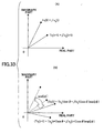
- Fig. 33 shows an example.
- feedback signals corresponding to the digital signals Tx(t) and Tx(t+1) are shown.
- the influence of the orthogonality deflection ⁇ and the influence of the phase rotation ⁇ are reflected in the feedback signals.
- the asterisk "*" means a complex conjugate
- Im[] means the imaginary part of the argument.
- the imaginary part of the inner product of the feedback signal corresponding to the digital signals Tx(t) and Tx(t+1) is expressed as follows.
- the orthogonality deflection ⁇ is obtained by the following formula.
- ⁇ cos -1 (Im[inner product of the feedback signal]/Im[inner product of the signals before quadrature modulation]).
- Embodiment 4 wherein the timing, amplitude, and angle deflection of the inphase signal component and the orthogonal signal component are collectively adjusted.
- Fig. 34 is a block diagram of the quadrature modulation system according to Embodiment 4 of the present invention.
- the quadrature modulation system includes a compensation circuit 3402, digital-to-analog converters 3404 and 3406, and a quadrature modulator 3412.
- the quadrature modulation system includes an analog-to-digital converter 3418, a quadrature demodulator 3420, and a mismatching amount calculation unit 3422.
- the digital-to-analog converters 3404 and 3406 convert the inphase signal component and the orthogonal signal component, respectively, from digital to analog format.
- the quadrature modulator 3412 combines the inphase signal component and the orthogonal signal component that are provided by the respective digital-to-analog converters, and outputs an output signal.
- the analog-to-digital converter 3418 converts the output signal, which is an analog signal, into a digital signal.
- the quadrature demodulator 3420 carries out the quadrature demodulation of the output of the analog-to-digital converter 3418, and outputs the inphase signal component Fb i and the orthogonal signal component Fbq of the feedback signal.
- the mismatching amount calculation unit 3422 calculates amounts of mismatching (differences) between the inphase signal component and the orthogonal signal component, namely, timing difference, orthogonality deflection, and amplitude difference based on the digital signal Tx before quadrature modulation and the feedback signal Fb.
- the amounts of mismatching are provided to the compensation circuit 3402 such that the mismatching is compensated for.
- the mismatching amount calculation unit 3422 includes a delay circuit 3424, multiplying units 3426, 3428, 3430, and 3432, integrators 3434, 3436, 3438, and 3440, and a compensation value calculation circuit 3442.
- the integrator 3434 outputs E[Tx i (t) ⁇ Fb i (t)] as an output P.
- E[] is an expression of equalization, and is obtained by dividing a value totaled by the integrator by a suitable factor. Assuming that the inphase and the orthogonal signal components are not correlated to each other, the output P is approximated as follows.
- ⁇ t represents the timing difference between the inphase and the orthogonal signal components
- ⁇ represents a phase rotation angle
- ⁇ represents an orthogonality deflection of the real axis and the imaginary axis.
- the integrator 3436 outputs an output Q, which is equal to E[Tx i (t) ⁇ Fb q (t)]
- the integrator 3438 outputs an output R, which is equal to E [Tx q (t) ⁇ Fbi (t) ]
- the integrator 3440 outputs an output S, which is equal to E[Tx q (t) ⁇ Fbq(t)].
- Q, R, and S are approximated as follows.
- P 2 +Q 2 and R 2 +S 2 are calculated by the compensation value calculation circuit 3442, which are expressed as follows.
- P 2 +Q 2 and R 2 +S 2 are not dependent on the phase rotation angle ⁇ , nor the orthogonality deflection ⁇ . Therefore, it becomes possible to calculate an optimal amount of delay by monitoring and comparing these values, with the delay circuit 3424 gradually changing the amount of the delay.
- the amplitude difference can be determined by other methods such as determining the difference between the amplitudes (
- phase rotation angle ⁇ and the orthogonality deflection ⁇ are determined using the following formulas.
- the time difference, the amplitude difference, and the orthogonality deflection that are obtained by the compensation value calculation circuit 3422 are provided to the compensation circuit 3422 such that the differences are compensated for.
- Fig. 35 is a block diagram of the quadrature modulation system according to another embodiment of the present invention.
- the quadrature modulation system includes a compensation circuit 3502, digital-to-analog converters 3504 and 3506, and a quadrature modulator 3512.
- the quadrature modulation system includes an analog-to-digital converter 3518, a quadrature demodulator 3520, a mismatching amount calculation unit 3522, and a phase detector 3544.
- the digital-to-analog converters 3504 and 3506 convert the inphase signal component and the orthogonal signal component, respectively, from digital to analog format.
- the quadrature modulator 3512 combines the inphase signal component and the orthogonal signal component that are provided by the respective digital-to-analog converters, and outputs an output signal.
- the analog-to-digital converter 3518 converts the down-converted signal, which is an analog signal, into a digital signal.
- the quadrature demodulator 3520 carries out the quadrature demodulation of the output of the analog-to-digital converter 3518, and outputs the inphase signal component Fb i and the orthogonal signal component Fbq of the feedback signal.
- the mismatching amount calculation unit 3522 calculates the amounts of mismatching between the inphase signal component and the orthogonal signal component, namely, the timing difference, orthogonality deflection, and amplitude difference, based on the digital signal Tx before quadrature modulation and the feedback signal Fb.
- the amounts of mismatching are provided to the compensation circuit 3502 such that the mismatching is compensated for.
- the mismatching amount calculation unit 3522 includes a delay circuit 3524, multiplying units 3526, 3528, 3530, and 3532, integrators 3534, 3536, 3538, and 3540, and a compensation value calculation circuit 3542. Further, the mismatching amount calculation unit 3522 includes subtractors 3546, 3550, 3554, and 3558. Further, the mismatching amount calculation unit 3522 includes multiplying units 3548, 3552, 3556, and 3560 for inserting weights ⁇ , ⁇ 2 , ⁇ 3 , and ⁇ 4 .
- the mismatching amount calculation unit 3522 includes the multiplying units 3548, 3552, 3556, and 3560 for introducing the weights ⁇ , ⁇ 2 , ⁇ 3 , and ⁇ 4 , and the phase detector 3544.
- P, Q, R, and S in the case shown by Fig. 34 are as follows.
- P E[Tx i (t) ⁇ Fb i (t)]
- Q E[Tx i (t) ⁇ Fb q (t)]
- R E[Tx q (t) ⁇ Fb i (t)]
- S E[Tx q (t) ⁇ Fb q (t)]
Landscapes
- Engineering & Computer Science (AREA)
- Computer Networks & Wireless Communication (AREA)
- Signal Processing (AREA)
- Digital Transmission Methods That Use Modulated Carrier Waves (AREA)
- Amplitude Modulation (AREA)
- Signal Processing For Digital Recording And Reproducing (AREA)
Abstract
Description
[Patent reference 1] JPA 6-350658
[Patent reference 2] JPA 7-123123
[Patent reference 3] JPA 7-177188
[Patent reference 4] JPA 8-116343
[Patent reference 5] JPA 2000-270037
[Patent reference 6] JPA 2001-339452
[Patent reference 7] JPA 2002-27007
[Patent reference 8] JPA 5-207080
[Patent reference 9] JPA 2002-77285
[Patent reference 10] JPA 8-97873
[Problem(s) to be solved by the Invention]


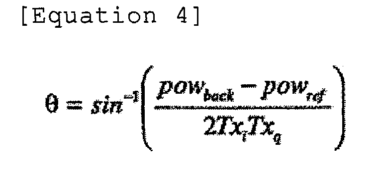
Claims (25)
- A quadrature modulation system wherein a first inphase signal component and a first orthogonal signal component are input, and are provided to a quadrature modulator for outputting an output signal that is quadrature modulated by the quadrature modulator, a part of said output signal serving as a feedback signal consisting of a second inphase signal component and a second orthogonal signal component, comprising:time difference calculating means forobtaining a first cumulative total of results of calculation based on the first inphase signal component and the second inphase signal component,obtaining a second cumulative total of results of calculation based on the first orthogonal signal component and the second orthogonal signal component, andobtaining a time difference between the first inphase signal component and the second inphase signal component, and a time difference between the first orthogonal signal component and the second orthogonal signal component based on said first cumulative total and said second cumulative total, respectively; anddelay adjustment means for adjusting the first inphase signal component and the first orthogonal signal component that are provided to the quadrature modulator such that said time differences are compensated for.
- The quadrature modulation system as claimed in claim 1, wherein said calculation calculates one of a difference between and a product of the first inphase signal component and the second inphase signal component, and one of a difference between and a product of the first orthogonal signal component and the second orthogonal signal component.
- The quadrature modulation system as claimed in claim 1, further comprising:means for comparing the first inphase signal component and the first orthogonal signal component with the second inphase signal component and the second orthogonal signal component, respectively, and for obtaining a rotation angle of the real axis and the imaginary axis of a signal point arrangement.
- The quadrature modulation system as claimed in claim 1, wherein said delay adjustment means comprises:a finite impulse response filter, a tap coefficient of which is changeable according to said time difference.
- The quadrature modulation system as claimed in claim 1, wherein said delay adjustment means carries forward or delays a clock signal according to said time difference, the clock signal being provided to at least one of digital-to-analog converters for converting the first inphase signal component and the first orthogonal signal component into respective analog signal components.
- A quadrature modulation system wherein a first inphase signal component and a first orthogonal signal component are input, and are provided to a quadrature modulator for outputting an output signal that is quadrature modulated by the quadrature modulator, a part of said output signal serving as a feedback signal consisting of a second inphase signal component and a second orthogonal signal component, comprising:amplitude difference calculation means forobtaining a first error that is a difference between average amplitudes of the second inphase signal component and the second orthogonal signal component,obtaining a second error that is a difference between average amplitudes of the second inphase signal component and the second orthogonal signal component when the real axis and the imaginary axis of a signal point arrangement are rotated by a predetermined angle amount, andfor obtaining an amount of amplitude difference between the first inphase signal component and the first orthogonal signal component based on said first error and said second error; andamplitude adjustment means for adjusting the amplitudes of the first inphase signal component and the first orthogonal signal component such that the amplitude difference is compensated for.
- The quadrature modulation system as claimed in claim 6, further comprising:means for comparing the magnitude of said first error with the magnitude of said second error.
- The quadrature modulation system as claimed in claim 6, wherein said predetermined angle amount is substantially equal to 45 degrees.
- A quadrature modulation system wherein an inphase signal component and an orthogonal signal component are input, and are provided to a quadrature modulator for outputting an output signal that is quadrature modulated by the quadrature modulator, comprising:means for obtaining an average amplitude vector of the inphase signal component and the orthogonal signal component for every quadrant of a signal point arrangement; andamplitude adjustment means for adjusting the amplitudes of the inphase signal component and the orthogonal signal component that are provided to said quadrature modulator such that the average amplitude vectors of the quadrants become equal in magnitude to each other, and orthogonally intersect.
- A quadrature modulation system wherein a first inphase signal component and a first orthogonal signal component are input, and are provided to a quadrature modulator for outputting an output signal that is quadrature modulated by the quadrature modulator, a part of said output signal serving as a feedback signal consisting of a second inphase signal component and a second orthogonal signal component, comprising:amplitude difference calculation means forobtaining a first error that is a difference between an average amplitude of the first inphase signal component and an average amplitude of the second inphase signal component,obtaining a second error that is a difference between an average amplitude of the first orthogonal signal component and an average amplitude of the second orthogonal signal component, andobtaining an amount of difference between the amplitude of the first inphase signal component and the amplitude of the first orthogonal signal component based on said first error and said second error, respectively; andamplitude adjustment means for adjusting the amplitudes of the first inphase signal component and the first orthogonal signal component such that the differences of said amplitudes are compensated for.
- The quadrature modulation system as claimed in claim 10, further comprising:means for comparing the first inphase signal component and the first orthogonal signal component with the second inphase signal component and the second orthogonal signal component, respectively, and for obtaining a rotation angle of the real axis and the imaginary axis of a signal point arrangement.
- A quadrature modulation system wherein a first inphase signal component and a first orthogonal signal component are input, and are provided to a quadrature modulator for outputting an output signal that is quadrature modulated by the quadrature modulator, a part of said output signal serving as a feedback signal consisting of a second inphase signal component and a second orthogonal signal component, comprising:amplitude difference calculation means forobtaining a first average that is an average of products of the first inphase signal component and the second orthogonal signal component,obtaining a second average that is an average of products of the first orthogonal signal component provided and the second inphase signal component, andobtaining a value that is proportional to a ratio of the first average to the second average; andamplitude adjustment means for adjusting the first inphase signal component and the first orthogonal signal component such that the value that is proportional to said ratio approaches a desired value.
- The quadrature modulation system as claimed in any one of claims 1, 6, 9, and 12, wherein
the first inphase signal component and the first orthogonal signal component, amplitudes of which components are adjusted by the adjustment means are in one of digital format and analog format. - A quadrature modulation system wherein a first inphase signal component and a first orthogonal signal component are input, and are provided to a quadrature modulator for outputting an output signal that is quadrature modulated by the quadrature modulator, a part of said output signal serving as a feedback signal consisting of a second inphase signal component and a second orthogonal signal component, comprising:angle deflection calculation means forobtaining an amount of difference between a cumulative total of the second inphase signal component and a cumulative total of the second orthogonal signal component, andcalculating an amount of angle deflection between the real axis and the imaginary axis of a signal point arrangement based on said amount of difference; andadjustment means for adjusting the first inphase signal component and the first orthogonal signal component such that said angle deflection is compensated for.
- A quadrature modulation system wherein a first inphase signal component and a first orthogonal signal component are input, and are provided to a quadrature modulator for outputting an output signal that is quadrature modulated by the quadrature modulator, a part of said output signal serving as a feedback signal consisting of a second inphase signal component and a second orthogonal signal component, comprising:angle deflection calculation means for obtaining an amount of angle deflection between the real axis and the imaginary axis of a signal point arrangement based on a cumulative total of products of the second inphase signal component and the second orthogonal signal; andadjustment means for adjusting the first inphase signal component and the first orthogonal signal component such that said angle deflection is compensated for.
- A quadrature modulation system wherein a first inphase signal component and a first orthogonal signal component are input, and are provided to a quadrature modulator for outputting an output signal that is quadrature modulated by the quadrature modulator, a part of said output signal serving as a feedback signal consisting of a second inphase signal component and a second orthogonal signal component, comprising:angle deflection calculation means forobtaining a first cumulative total that is a cumulative total of values representing differences between the first inphase signal component and the second inphase signal component,obtaining a second cumulative total of values representing differences between the first orthogonal signal component and the second orthogonal signal component, andobtaining an amount of angle deflection between the real axis and the imaginary axis of a signal point arrangement based on the first cumulative total and the second cumulative total; andadjustment means for adjusting the first inphase signal component and the first orthogonal signal component such that said angle deflection is compensated for.
- A quadrature modulation system wherein a first inphase signal component and a first orthogonal signal component are input, and are provided to a quadrature modulator for outputting an output signal that is quadrature modulated by the quadrature modulator, a part of said output signal serving as a feedback signal consisting of a second inphase signal component and a second orthogonal signal component, comprising:angle deflection calculation means for obtaining a power difference that is adifference between power of a signal provided to said quadrature modulator and power of the feedback signal,obtaining a signal product that is a product of the first inphase signal component and the first orthogonal signal component of the signal provided to said quadrature modulator, andobtaining an amount of the angle deflection between the real axis and the imaginary axis of a signal point arrangement based on a ratio of said power difference to said signal product; andadjustment means for adjusting the first inphase signal component and the first orthogonal signal component such that said angle deflection is compensated for.
- The quadrature modulation system as claimed in claim 17, wherein said angle deflection calculation means obtains said angle deflection by using an arc-sine function, to the argument of which the ratio of said power difference to said signal product is substituted.
- A quadrature modulation system wherein a first inphase signal component and a first orthogonal signal component are input, and are provided to a quadrature modulator for outputting an output signal that is quadrature modulated by the quadrature modulator, a part of said output signal serving as a feedback signal consisting of a second inphase signal component and a second orthogonal signal component, comprising:angle deflection calculation means forobtaining a first value that expresses the imaginary part of an inner product of a first signal at a first point in time and a second signal at a second point in time, the first and second signals being provided to said quadrature modulator,obtaining a second value that expresses the imaginary part of an inner product of the feedback signals corresponding to said first signal and second signal, andobtaining an amount of the angle deflection between the real axis and the imaginary axis in a signal point arrangement based on a ratio of the first value to the second quantity; andadjustment means for adjusting the first inphase signal component and the first orthogonal signal component that such that said angle deflection is compensated for.
- The quadrature modulation system as claimed in claim 19, wherein said angle deflection calculation means obtains said angle deflection by using an arc-cosine function, to the argument of which the ratio of the first value to the second value is substituted.
- A quadrature modulation system wherein a first inphase signal component and a first orthogonal signal component are input, and are provided to a quadrature modulator for outputting an output signal that is quadrature modulated by the quadrature modulator, a part of said output signal serving as a feedback signal consisting of a second inphase signal component and a second orthogonal signal component, comprising:mismatch amount calculation means forcarrying out Fourier transformation of the feedback signal,detecting an unnecessary signal component contained in said feedback signal, andcalculating at least one mismatch amount of a time difference between the first inphase signal component and the first orthogonal signal component, an amount of amplitude difference between the first inphase signal component and the first orthogonal signal component, and an angle deflection between the real axis and the imaginary axis of a signal point arrangement based on said unnecessary signal component; andadjustment means for adjusting the first inphase signal component and the first orthogonal signal component such that said amount of mismatching is compensated for.
- A quadrature modulation system wherein a first inphase signal component and a first orthogonal signal component are input, and are provided to a quadrature modulator for outputting an output signal that is quadrature modulated by the quadrature modulator, a part of said output signal serving as a feedback signal consisting of a second inphase signal component and a second orthogonal signal component, comprising:means for calculating a first average that is an average of products of the first inphase signal component and the second inphase signal component;means for calculating a second average that is an average of products of the first inphase signal component and the second orthogonal signal component;means for calculating a third average that is an average of products of the first orthogonal signal component and the second inphase signal component;means for calculating a fourth average that is an average of products of the first orthogonal signal component and the second orthogonal signal component;mismatch amount calculation means for obtaining at least one of mismatch amounts of a time difference between the first inphase signal component and the first orthogonal signal component, an amount of amplitude difference between the first inphase signal component and the first orthogonal signal component, and an angle deflection between the real axis and the imaginary axis of a signal point arrangement based on the first average, the second average, the third average, and the fourth average; andadjustment means for adjusting the first inphase signal component and the first orthogonal signal component such that said amount of mismatching is compensated for.
- The quadrature modulation system as claimed in claim 22, wherein said mismatch amount calculation means comprises:time difference calculating means for obtaining the time difference between the first inphase signal component and the first orthogonal signal component based on comparison of a sum of a square of the first average and a square of the second average, and a sum of a square of the third average and a square of the fouth average, respectively;amplitude difference calculation means forobtaining a first ratio that is a ratio of a mean-square value of the first inphase signal component to a square root of a sum of a square of the first average and a square of the second average,obtaining a second ratio that is a ratio of the mean-square value of the first orthogonal signal component to a square root of a sum of a square of the third average and a square of the fouth average, andobtaining an amount of the amplitude difference between the first inphase signal component and the first orthogonal signal component based on the first and the second ratios; andangle deflection calculation means for obtaining the angle deflection between the real axis and the imaginary axis of the signal point arrangement based on a ratio of the first average and the second average, and a ratio of the third average and the fouth average.
- The quadrature modulation system as claimed in claim 22, wherein the first, the second, the third, and the fouth averages of the feedback signal are obtained with the real axis and the imaginary axis of the signal point arrangement being rotated by a predetermined angle.
- A transmitter comprising the quadrature modulation system as claimed in any one of claims 1-12 and 14-24.
Priority Applications (1)
| Application Number | Priority Date | Filing Date | Title |
|---|---|---|---|
| EP12171361A EP2501091A3 (en) | 2004-04-21 | 2004-09-17 | A quadrature modulation system |
Applications Claiming Priority (2)
| Application Number | Priority Date | Filing Date | Title |
|---|---|---|---|
| JP2004125849 | 2004-04-21 | ||
| JP2004125849A JP4376689B2 (en) | 2004-04-21 | 2004-04-21 | Quadrature modulation system |
Related Child Applications (2)
| Application Number | Title | Priority Date | Filing Date |
|---|---|---|---|
| EP12171361A Division EP2501091A3 (en) | 2004-04-21 | 2004-09-17 | A quadrature modulation system |
| EP12171361.4 Division-Into | 2012-06-08 |
Publications (2)
| Publication Number | Publication Date |
|---|---|
| EP1589713A2 true EP1589713A2 (en) | 2005-10-26 |
| EP1589713A3 EP1589713A3 (en) | 2013-04-10 |
Family
ID=34930666
Family Applications (2)
| Application Number | Title | Priority Date | Filing Date |
|---|---|---|---|
| EP12171361A Withdrawn EP2501091A3 (en) | 2004-04-21 | 2004-09-17 | A quadrature modulation system |
| EP04255686.0A Withdrawn EP1589713A3 (en) | 2004-04-21 | 2004-09-17 | Quadrature modulator with compensation of I/Q mismatch |
Family Applications Before (1)
| Application Number | Title | Priority Date | Filing Date |
|---|---|---|---|
| EP12171361A Withdrawn EP2501091A3 (en) | 2004-04-21 | 2004-09-17 | A quadrature modulation system |
Country Status (4)
| Country | Link |
|---|---|
| US (1) | US7388926B2 (en) |
| EP (2) | EP2501091A3 (en) |
| JP (1) | JP4376689B2 (en) |
| CN (3) | CN100571246C (en) |
Cited By (3)
| Publication number | Priority date | Publication date | Assignee | Title |
|---|---|---|---|---|
| WO2008150702A1 (en) * | 2007-05-30 | 2008-12-11 | Motorola, Inc. | Method and apparatus for generating corrected quadrature phase signal pairs in a communication device |
| WO2010124298A3 (en) * | 2009-04-24 | 2011-04-21 | Qualcomm Incorporated | I/q imbalance estimation and compensation for a transmitter and a receiver |
| EP1838064A3 (en) * | 2006-03-22 | 2013-03-06 | Fujitsu Limited | Apparatus and method for I-Q quadrature modulation transmitter and its I-Q phase bias monitoring |
Families Citing this family (21)
| Publication number | Priority date | Publication date | Assignee | Title |
|---|---|---|---|---|
| JP4299819B2 (en) * | 2005-08-17 | 2009-07-22 | 富士通株式会社 | Distortion compensation apparatus and distortion compensation method |
| US8345801B2 (en) * | 2005-11-10 | 2013-01-01 | Weon-Ki Yoon | Apparatus and method for signal mismatch compensation in a wireless receiver |
| JP4659621B2 (en) * | 2006-01-06 | 2011-03-30 | 株式会社日立国際電気 | Wireless transmitter |
| US8693525B2 (en) | 2006-07-14 | 2014-04-08 | Qualcomm Incorporated | Multi-carrier transmitter for wireless communication |
| US7974596B2 (en) * | 2006-09-22 | 2011-07-05 | Silicon Laboratories Inc. | Power control scheme for a power amplifier |
| JP4803379B2 (en) * | 2006-11-09 | 2011-10-26 | 日本電気株式会社 | Wireless transmission device with quadrature modulator |
| KR100809206B1 (en) * | 2006-11-30 | 2008-02-29 | 삼성전기주식회사 | Time Domain IV Mismatch Detection of Orthogonal Frequency Division Multiple Receivers |
| CN101873446B (en) * | 2009-04-22 | 2012-05-16 | 承景科技股份有限公司 | Digital receiver and related method |
| JP5158034B2 (en) * | 2009-08-12 | 2013-03-06 | 富士通株式会社 | Wireless device and signal processing method |
| WO2011054156A1 (en) * | 2009-11-09 | 2011-05-12 | 华为技术有限公司 | Method, device and system for correcting microwave signal |
| JP5091979B2 (en) * | 2010-04-30 | 2012-12-05 | 株式会社エヌ・ティ・ティ・ドコモ | User apparatus and method in wireless communication system |
| WO2011161877A1 (en) * | 2010-06-24 | 2011-12-29 | 日本電気株式会社 | Modem and amplitude adjustment method |
| JP5516378B2 (en) * | 2010-12-13 | 2014-06-11 | 富士通株式会社 | Distortion compensation apparatus, distortion compensation method, and radio apparatus |
| US9077571B2 (en) | 2011-09-09 | 2015-07-07 | Nxp B.V. | Adaptive equalizer and/or antenna tuning |
| WO2013067291A1 (en) | 2011-11-02 | 2013-05-10 | Raytheon Company | Quadrature modulator balancing system |
| TWI448090B (en) * | 2012-02-17 | 2014-08-01 | Inst Information Industry | Receiver having inphase-quadrature imbalance compensation and inphase-quadrature imbalance compensation method thereof |
| RU2546304C1 (en) * | 2014-01-24 | 2015-04-10 | Закрытое акционерное общество "Проектно-конструкторское бюро "РИО" | Apparatus of generating quadrature amplitude-shift keyed signals |
| RU2547626C1 (en) * | 2014-02-10 | 2015-04-10 | Закрытое акционерное общество "Проектно-конструкторское бюро "РИО" | Apparatus of generating quadrature amplitude-shift keyed signals |
| US9491029B2 (en) * | 2014-12-15 | 2016-11-08 | Apple Inc. | Devices and methods for reducing signal distortion in I/Q modulation transceivers |
| WO2017051218A1 (en) * | 2015-09-25 | 2017-03-30 | Intel IP Corporation | An apparatus and a method for generating a radio frequency signal |
| US10516563B2 (en) | 2015-09-25 | 2019-12-24 | Intel IP Corporation | Apparatus and a method for generating a radio frequency signal |
Family Cites Families (25)
| Publication number | Priority date | Publication date | Assignee | Title |
|---|---|---|---|---|
| US4717894A (en) * | 1986-10-23 | 1988-01-05 | Hewlett-Packard Company | Calibration of vector modulators using a scalar detector |
| DE69222452T2 (en) * | 1991-03-11 | 1998-02-26 | Nippon Telegraph & Telephone | Quadrature amplitude modulator with distortion compensation |
| JP3259100B2 (en) | 1992-01-24 | 2002-02-18 | 日本電気エンジニアリング株式会社 | Modulator |
| JP3037025B2 (en) | 1993-06-10 | 2000-04-24 | 松下電器産業株式会社 | Quadrature modulator |
| JP3552254B2 (en) | 1993-10-25 | 2004-08-11 | ソニー株式会社 | Four-phase modulation circuit |
| JPH07177188A (en) | 1993-12-17 | 1995-07-14 | Nippon Motorola Ltd | Quadrature modulation / demodulation system with modulation accuracy compensation function |
| JPH0897873A (en) | 1994-09-28 | 1996-04-12 | Nec Corp | Orthogonal modulator |
| JPH08116343A (en) | 1994-10-17 | 1996-05-07 | Mitsubishi Electric Corp | Quadrature modulator |
| JPH09186729A (en) * | 1996-01-08 | 1997-07-15 | Hitachi Denshi Ltd | Amplitude error control method for quadrature modulator and quadrature demodulator |
| EP0795982B1 (en) * | 1996-03-11 | 2005-01-12 | Micronas GmbH | Transmission system with quadrature modulation |
| FI117494B (en) * | 1996-11-29 | 2006-10-31 | Nokia Corp | Procedure in a digital quadrature modulator and in a quadrature demodulator, digital quadrature modulator and quadrature demodulator |
| US6286994B1 (en) * | 1998-04-29 | 2001-09-11 | Qualcomm Incorporated | System, method and computer program product for controlling a transmit signal using an expected power level |
| US6054896A (en) * | 1998-12-17 | 2000-04-25 | Datum Telegraphic Inc. | Controller and associated methods for a linc linear power amplifier |
| JP2000270037A (en) | 1999-03-19 | 2000-09-29 | Hitachi Denshi Ltd | Quadrature modulator |
| FI107100B (en) * | 1999-03-26 | 2001-05-31 | Nokia Networks Oy | Correction of an I / Q modulator phase and amplitude imbalance |
| JP4097430B2 (en) * | 1999-07-28 | 2008-06-11 | 富士通株式会社 | Wireless device with distortion compensation function |
| JP2001339452A (en) | 2000-05-26 | 2001-12-07 | Hitachi Kokusai Electric Inc | Quadrature modulation device and quadrature modulation error detection method |
| JP2002027007A (en) | 2000-07-12 | 2002-01-25 | Matsushita Electric Ind Co Ltd | Error compensation method |
| US6934341B2 (en) * | 2000-08-29 | 2005-08-23 | Telefonaktiebolaget Lm Ericsson (Publ) | Method and apparatus for plurality signal generation |
| JP2002077285A (en) | 2000-08-31 | 2002-03-15 | Hitachi Kokusai Electric Inc | Transmitter |
| US7054375B2 (en) * | 2000-12-22 | 2006-05-30 | Nokia Corporation | Method and apparatus for error reduction in an orthogonal modulation system |
| JP2002208978A (en) * | 2001-01-05 | 2002-07-26 | Mitsubishi Electric Corp | Quadrature modulator |
| US7061994B2 (en) * | 2001-06-21 | 2006-06-13 | Flarion Technologies, Inc. | Methods and apparatus for I/Q imbalance compensation |
| EP1361655A1 (en) * | 2002-05-07 | 2003-11-12 | Semiconductor Ideas to The Market (ItoM) BV | Mirror suppression circuit in a quadrature demodulator |
| WO2004015853A1 (en) * | 2002-08-02 | 2004-02-19 | Nokia Corporation | Quadrature demodulator using a fft-processor |
-
2004
- 2004-04-21 JP JP2004125849A patent/JP4376689B2/en not_active Expired - Fee Related
- 2004-09-17 EP EP12171361A patent/EP2501091A3/en not_active Withdrawn
- 2004-09-17 EP EP04255686.0A patent/EP1589713A3/en not_active Withdrawn
- 2004-09-20 US US10/945,316 patent/US7388926B2/en not_active Expired - Fee Related
- 2004-09-30 CN CNB2004100831336A patent/CN100571246C/en not_active Expired - Fee Related
- 2004-09-30 CN CN2009102052423A patent/CN101677307B/en not_active Expired - Fee Related
- 2004-09-30 CN CN2009102052419A patent/CN101674271B/en not_active Expired - Fee Related
Cited By (4)
| Publication number | Priority date | Publication date | Assignee | Title |
|---|---|---|---|---|
| EP1838064A3 (en) * | 2006-03-22 | 2013-03-06 | Fujitsu Limited | Apparatus and method for I-Q quadrature modulation transmitter and its I-Q phase bias monitoring |
| WO2008150702A1 (en) * | 2007-05-30 | 2008-12-11 | Motorola, Inc. | Method and apparatus for generating corrected quadrature phase signal pairs in a communication device |
| US7742545B2 (en) | 2007-05-30 | 2010-06-22 | Motorola, Inc. | Method and apparatus for generating corrected quadrature phase signal pairs in a communication device |
| WO2010124298A3 (en) * | 2009-04-24 | 2011-04-21 | Qualcomm Incorporated | I/q imbalance estimation and compensation for a transmitter and a receiver |
Also Published As
| Publication number | Publication date |
|---|---|
| EP2501091A2 (en) | 2012-09-19 |
| US7388926B2 (en) | 2008-06-17 |
| CN101677307B (en) | 2012-11-07 |
| CN1691660A (en) | 2005-11-02 |
| EP1589713A3 (en) | 2013-04-10 |
| CN100571246C (en) | 2009-12-16 |
| JP4376689B2 (en) | 2009-12-02 |
| EP2501091A3 (en) | 2013-03-13 |
| US20050238114A1 (en) | 2005-10-27 |
| JP2005311710A (en) | 2005-11-04 |
| CN101674271A (en) | 2010-03-17 |
| CN101677307A (en) | 2010-03-24 |
| CN101674271B (en) | 2012-07-18 |
Similar Documents
| Publication | Publication Date | Title |
|---|---|---|
| EP1589713A2 (en) | Quadrature modulator with compensation of I/Q mismatch | |
| EP1777906A1 (en) | Amplitude error compensating apparatus and orthogonality error compensating apparatus | |
| US6771709B2 (en) | System and method for direct transmitter self-calibration | |
| JP3611862B2 (en) | Digital quadrature modulation and demodulation method, digital quadrature modulator and demodulator | |
| CN100481828C (en) | Amplitude imbalance compensation of quadrature modulator | |
| EP2381595B1 (en) | Phase skew compensation at a coherent optical receiver | |
| EP2498466A1 (en) | Carrier wave reproduction circuit and demodulation circuit of semi-synchronous detection system | |
| KR100581059B1 (en) | Apparatus and method for compensating phase and gain mismatch between in-phase channel and orthogonal channel using variable loop gain in orthogonal demodulation receiving system | |
| JPH07321868A (en) | Automatic frequency adjusting method and device thereof | |
| CN111884964B (en) | Frequency synchronization system adapting to VDE multi-modulation system | |
| US7031382B2 (en) | Non-linear equalizer system and method | |
| US6263028B1 (en) | Apparatus and method for measuring modulation accuracy | |
| US5684842A (en) | Digital transmission system comprising a receiver which includes a carrier recovery circuit | |
| US6473470B1 (en) | Phase-locked loop circuits for communication system | |
| US5663691A (en) | Estimator for estimating an operating defect in a quadrature modulator, and a modulation stage using the estimator | |
| US10250283B1 (en) | Digital frequency locked loop for wideband communications channels requiring extreme Doppler compensation and low signal to noise ratio | |
| EP2547059B1 (en) | Transmitter including calibration of an in-phase/Quadrature (I/Q) modulator and associated methods | |
| EP1060601B1 (en) | Demodulator having rotation means for frequency offset correction | |
| KR100760793B1 (en) | Correction of Orthogonal and Gain Errors in Synchronous Receivers | |
| JP3388079B2 (en) | Receiver | |
| JP2003087344A (en) | Direct conversion receiver | |
| Sarma et al. | A Closed Loop Quadrature Phase Detector for Phase and Frequency Discrimination along with Suppression of DC Bias | |
| JP2002247124A (en) | System and method for phase error correction | |
| JP2000059449A (en) | Method for estimating frequency errors in qpsk demodulator | |
| JP2011109520A (en) | Receiving machine |
Legal Events
| Date | Code | Title | Description |
|---|---|---|---|
| PUAI | Public reference made under article 153(3) epc to a published international application that has entered the european phase |
Free format text: ORIGINAL CODE: 0009012 |
|
| AK | Designated contracting states |
Kind code of ref document: A2 Designated state(s): AT BE BG CH CY CZ DE DK EE ES FI FR GB GR HU IE IT LI LU MC NL PL PT RO SE SI SK TR |
|
| AX | Request for extension of the european patent |
Extension state: AL HR LT LV MK |
|
| RIC1 | Information provided on ipc code assigned before grant |
Ipc: H04L 27/00 20060101ALI20121119BHEP Ipc: H04L 27/36 20060101AFI20121119BHEP |
|
| PUAL | Search report despatched |
Free format text: ORIGINAL CODE: 0009013 |
|
| AK | Designated contracting states |
Kind code of ref document: A3 Designated state(s): AT BE BG CH CY CZ DE DK EE ES FI FR GB GR HU IE IT LI LU MC NL PL PT RO SE SI SK TR |
|
| AX | Request for extension of the european patent |
Extension state: AL HR LT LV MK |
|
| RIC1 | Information provided on ipc code assigned before grant |
Ipc: H04L 27/36 20060101AFI20130301BHEP Ipc: H04L 27/00 20060101ALI20130301BHEP |
|
| 17P | Request for examination filed |
Effective date: 20130531 |
|
| RBV | Designated contracting states (corrected) |
Designated state(s): AT BE BG CH CY CZ DE DK EE ES FI FR GB GR HU IE IT LI LU MC NL PL PT RO SE SI SK TR |
|
| 17Q | First examination report despatched |
Effective date: 20130708 |
|
| AKX | Designation fees paid |
Designated state(s): DE FR GB |
|
| STAA | Information on the status of an ep patent application or granted ep patent |
Free format text: STATUS: THE APPLICATION IS DEEMED TO BE WITHDRAWN |
|
| 18D | Application deemed to be withdrawn |
Effective date: 20160401 |