EP1586616A2 - Organic electroluminescence device - Google Patents
Organic electroluminescence device Download PDFInfo
- Publication number
- EP1586616A2 EP1586616A2 EP05005801A EP05005801A EP1586616A2 EP 1586616 A2 EP1586616 A2 EP 1586616A2 EP 05005801 A EP05005801 A EP 05005801A EP 05005801 A EP05005801 A EP 05005801A EP 1586616 A2 EP1586616 A2 EP 1586616A2
- Authority
- EP
- European Patent Office
- Prior art keywords
- organic electroluminescence
- electroluminescence device
- transport layer
- layer
- hole injecting
- Prior art date
- Legal status (The legal status is an assumption and is not a legal conclusion. Google has not performed a legal analysis and makes no representation as to the accuracy of the status listed.)
- Granted
Links
- 238000005401 electroluminescence Methods 0.000 title claims abstract description 28
- 230000005525 hole transport Effects 0.000 claims abstract description 22
- 239000000463 material Substances 0.000 claims abstract description 15
- 239000000126 substance Substances 0.000 claims abstract description 11
- 125000003118 aryl group Chemical group 0.000 claims description 4
- ZUOUZKKEUPVFJK-UHFFFAOYSA-N diphenyl Chemical compound C1=CC=CC=C1C1=CC=CC=C1 ZUOUZKKEUPVFJK-UHFFFAOYSA-N 0.000 claims description 4
- 125000001495 ethyl group Chemical group [H]C([H])([H])C([H])([H])* 0.000 claims description 4
- 125000001449 isopropyl group Chemical group [H]C([H])([H])C([H])(*)C([H])([H])[H] 0.000 claims description 4
- 125000002496 methyl group Chemical group [H]C([H])([H])* 0.000 claims description 4
- 125000001436 propyl group Chemical group [H]C([*])([H])C([H])([H])C([H])([H])[H] 0.000 claims description 4
- 125000001424 substituent group Chemical group 0.000 claims description 4
- 239000004305 biphenyl Substances 0.000 claims description 3
- YJTKZCDBKVTVBY-UHFFFAOYSA-N 1,3-Diphenylbenzene Chemical group C1=CC=CC=C1C1=CC=CC(C=2C=CC=CC=2)=C1 YJTKZCDBKVTVBY-UHFFFAOYSA-N 0.000 claims description 2
- UFHFLCQGNIYNRP-UHFFFAOYSA-N Hydrogen Chemical compound [H][H] UFHFLCQGNIYNRP-UHFFFAOYSA-N 0.000 claims description 2
- 125000001931 aliphatic group Chemical group 0.000 claims description 2
- 125000003545 alkoxy group Chemical group 0.000 claims description 2
- 125000002877 alkyl aryl group Chemical group 0.000 claims description 2
- 125000000217 alkyl group Chemical group 0.000 claims description 2
- 125000005428 anthryl group Chemical group [H]C1=C([H])C([H])=C2C([H])=C3C(*)=C([H])C([H])=C([H])C3=C([H])C2=C1[H] 0.000 claims description 2
- 235000010290 biphenyl Nutrition 0.000 claims description 2
- 125000004093 cyano group Chemical group *C#N 0.000 claims description 2
- 125000000113 cyclohexyl group Chemical group [H]C1([H])C([H])([H])C([H])([H])C([H])(*)C([H])([H])C1([H])[H] 0.000 claims description 2
- 125000003983 fluorenyl group Chemical group C1(=CC=CC=2C3=CC=CC=C3CC12)* 0.000 claims description 2
- 229910052736 halogen Inorganic materials 0.000 claims description 2
- 150000002367 halogens Chemical class 0.000 claims description 2
- 125000005842 heteroatom Chemical group 0.000 claims description 2
- 229910052739 hydrogen Inorganic materials 0.000 claims description 2
- 239000001257 hydrogen Substances 0.000 claims description 2
- 125000005956 isoquinolyl group Chemical group 0.000 claims description 2
- -1 methoxy, ethoxy, propoxy, butoxy, fluoro, chloro, phenoxy, tolyloxy Chemical group 0.000 claims description 2
- 125000001624 naphthyl group Chemical group 0.000 claims description 2
- 125000005561 phenanthryl group Chemical group 0.000 claims description 2
- 125000001997 phenyl group Chemical group [H]C1=C([H])C([H])=C(*)C([H])=C1[H] 0.000 claims description 2
- 125000004076 pyridyl group Chemical group 0.000 claims description 2
- 125000005493 quinolyl group Chemical group 0.000 claims description 2
- 125000000999 tert-butyl group Chemical group [H]C([H])([H])C(*)(C([H])([H])[H])C([H])([H])[H] 0.000 claims description 2
- 239000010410 layer Substances 0.000 description 53
- YXFVVABEGXRONW-UHFFFAOYSA-N Toluene Chemical compound CC1=CC=CC=C1 YXFVVABEGXRONW-UHFFFAOYSA-N 0.000 description 36
- YMWUJEATGCHHMB-UHFFFAOYSA-N Dichloromethane Chemical compound ClCCl YMWUJEATGCHHMB-UHFFFAOYSA-N 0.000 description 33
- 239000000243 solution Substances 0.000 description 18
- 239000000758 substrate Substances 0.000 description 14
- 239000011521 glass Substances 0.000 description 12
- 229940073584 methylene chloride Drugs 0.000 description 11
- 239000002904 solvent Substances 0.000 description 11
- TVIVIEFSHFOWTE-UHFFFAOYSA-K tri(quinolin-8-yloxy)alumane Chemical compound [Al+3].C1=CN=C2C([O-])=CC=CC2=C1.C1=CN=C2C([O-])=CC=CC2=C1.C1=CN=C2C([O-])=CC=CC2=C1 TVIVIEFSHFOWTE-UHFFFAOYSA-K 0.000 description 9
- 238000006243 chemical reaction Methods 0.000 description 8
- VLKZOEOYAKHREP-UHFFFAOYSA-N n-Hexane Chemical compound CCCCCC VLKZOEOYAKHREP-UHFFFAOYSA-N 0.000 description 7
- 238000010898 silica gel chromatography Methods 0.000 description 7
- OKKJLVBELUTLKV-UHFFFAOYSA-N Methanol Chemical compound OC OKKJLVBELUTLKV-UHFFFAOYSA-N 0.000 description 6
- MVPPADPHJFYWMZ-UHFFFAOYSA-N chlorobenzene Chemical compound ClC1=CC=CC=C1 MVPPADPHJFYWMZ-UHFFFAOYSA-N 0.000 description 6
- MFRIHAYPQRLWNB-UHFFFAOYSA-N sodium tert-butoxide Chemical compound [Na+].CC(C)(C)[O-] MFRIHAYPQRLWNB-UHFFFAOYSA-N 0.000 description 6
- 230000008901 benefit Effects 0.000 description 5
- YJVFFLUZDVXJQI-UHFFFAOYSA-L palladium(ii) acetate Chemical compound [Pd+2].CC([O-])=O.CC([O-])=O YJVFFLUZDVXJQI-UHFFFAOYSA-L 0.000 description 5
- RTZKZFJDLAIYFH-UHFFFAOYSA-N Diethyl ether Chemical compound CCOCC RTZKZFJDLAIYFH-UHFFFAOYSA-N 0.000 description 4
- MUALRAIOVNYAIW-UHFFFAOYSA-N binap Chemical compound C1=CC=CC=C1P(C=1C(=C2C=CC=CC2=CC=1)C=1C2=CC=CC=C2C=CC=1P(C=1C=CC=CC=1)C=1C=CC=CC=1)C1=CC=CC=C1 MUALRAIOVNYAIW-UHFFFAOYSA-N 0.000 description 4
- 230000015572 biosynthetic process Effects 0.000 description 4
- 238000004020 luminiscence type Methods 0.000 description 4
- 239000007787 solid Substances 0.000 description 4
- 238000003786 synthesis reaction Methods 0.000 description 4
- OCQFHFNWMCLWKC-UHFFFAOYSA-N 1-n,4-n,4-n-triphenylbenzene-1,4-diamine Chemical compound C=1C=C(N(C=2C=CC=CC=2)C=2C=CC=CC=2)C=CC=1NC1=CC=CC=C1 OCQFHFNWMCLWKC-UHFFFAOYSA-N 0.000 description 3
- VEKBUQJHJXCFAB-UHFFFAOYSA-N 1-n,4-n-bis(3-bromophenyl)-1-n,4-n-diphenylbenzene-1,4-diamine Chemical compound BrC1=CC=CC(N(C=2C=CC=CC=2)C=2C=CC(=CC=2)N(C=2C=CC=CC=2)C=2C=C(Br)C=CC=2)=C1 VEKBUQJHJXCFAB-UHFFFAOYSA-N 0.000 description 3
- SQTLUXJWUCHKMT-UHFFFAOYSA-N 4-bromo-n,n-diphenylaniline Chemical compound C1=CC(Br)=CC=C1N(C=1C=CC=CC=1)C1=CC=CC=C1 SQTLUXJWUCHKMT-UHFFFAOYSA-N 0.000 description 3
- 0 CCCN(c1ccccc1)c(cc1)ccc1N(*)* Chemical compound CCCN(c1ccccc1)c(cc1)ccc1N(*)* 0.000 description 3
- 239000010405 anode material Substances 0.000 description 3
- 238000000034 method Methods 0.000 description 3
- 239000011368 organic material Substances 0.000 description 3
- 238000010992 reflux Methods 0.000 description 3
- KZPYGQFFRCFCPP-UHFFFAOYSA-N 1,1'-bis(diphenylphosphino)ferrocene Chemical compound [Fe+2].C1=CC=C[C-]1P(C=1C=CC=CC=1)C1=CC=CC=C1.C1=CC=C[C-]1P(C=1C=CC=CC=1)C1=CC=CC=C1 KZPYGQFFRCFCPP-UHFFFAOYSA-N 0.000 description 2
- WQONPSCCEXUXTQ-UHFFFAOYSA-N 1,2-dibromobenzene Chemical compound BrC1=CC=CC=C1Br WQONPSCCEXUXTQ-UHFFFAOYSA-N 0.000 description 2
- PAYRUJLWNCNPSJ-UHFFFAOYSA-N Aniline Chemical compound NC1=CC=CC=C1 PAYRUJLWNCNPSJ-UHFFFAOYSA-N 0.000 description 2
- DMBHHRLKUKUOEG-UHFFFAOYSA-N diphenylamine Chemical compound C=1C=CC=CC=1NC1=CC=CC=C1 DMBHHRLKUKUOEG-UHFFFAOYSA-N 0.000 description 2
- 239000002019 doping agent Substances 0.000 description 2
- 239000012535 impurity Substances 0.000 description 2
- ZGEGCLOFRBLKSE-UHFFFAOYSA-N methylene hexane Natural products CCCCCC=C ZGEGCLOFRBLKSE-UHFFFAOYSA-N 0.000 description 2
- 238000012986 modification Methods 0.000 description 2
- 230000004048 modification Effects 0.000 description 2
- 239000012044 organic layer Substances 0.000 description 2
- 239000003208 petroleum Substances 0.000 description 2
- XLYOFNOQVPJJNP-UHFFFAOYSA-N water Substances O XLYOFNOQVPJJNP-UHFFFAOYSA-N 0.000 description 2
- PAZVJIOFFOOQLQ-UHFFFAOYSA-N CCCN(CC)c1ccccc1 Chemical compound CCCN(CC)c1ccccc1 PAZVJIOFFOOQLQ-UHFFFAOYSA-N 0.000 description 1
- IQEPEDWTXSWNQV-UHFFFAOYSA-N COc(cc1)ccc1N(c1ccccc1)c(cc1)ccc1N(c1ccccc1)c(cc1)ccc1N(c1ccccc1)c(cc1)ccc1N(c1ccccc1)c(cc1)ccc1N(c1ccccc1)c(cc1)ccc1OC Chemical compound COc(cc1)ccc1N(c1ccccc1)c(cc1)ccc1N(c1ccccc1)c(cc1)ccc1N(c1ccccc1)c(cc1)ccc1N(c1ccccc1)c(cc1)ccc1N(c1ccccc1)c(cc1)ccc1OC IQEPEDWTXSWNQV-UHFFFAOYSA-N 0.000 description 1
- FLUWEVWHURLMFJ-UHFFFAOYSA-N Cc1ccc(C(c2ccccc2)c(cc2)ccc2N(c2ccccc2)c(cc2)ccc2N(c2ccccc2)c(cc2)ccc2N(c2ccccc2)c2ccc(CC(c3ccccc3)c(cc3)ccc3N(c3ccccc3)c3ccccc3)cc2)cc1 Chemical compound Cc1ccc(C(c2ccccc2)c(cc2)ccc2N(c2ccccc2)c(cc2)ccc2N(c2ccccc2)c(cc2)ccc2N(c2ccccc2)c2ccc(CC(c3ccccc3)c(cc3)ccc3N(c3ccccc3)c3ccccc3)cc2)cc1 FLUWEVWHURLMFJ-UHFFFAOYSA-N 0.000 description 1
- ZBJROCDVAWAHOG-UHFFFAOYSA-N Cc1ccc(CC(c2ccccc2)c(cc2)ccc2N(c2ccccc2)c(cc2)ccc2Br)cc1 Chemical compound Cc1ccc(CC(c2ccccc2)c(cc2)ccc2N(c2ccccc2)c(cc2)ccc2Br)cc1 ZBJROCDVAWAHOG-UHFFFAOYSA-N 0.000 description 1
- SHTWBYUBYHNVNR-UHFFFAOYSA-O Cc1cccc(N(c(cc2)ccc2N(c2ccccc2)c(cc2)ccc2N(c2ccccc2)c(cc2)ccc2N(c2ccccc2)c(cc2)ccc2N(c2ccccc2)c(cc2)ccc2[NH+](c2cccc(C)c2)c2cccc3c2cccc3)c2c(cccc3)c3ccc2)c1 Chemical compound Cc1cccc(N(c(cc2)ccc2N(c2ccccc2)c(cc2)ccc2N(c2ccccc2)c(cc2)ccc2N(c2ccccc2)c(cc2)ccc2N(c2ccccc2)c(cc2)ccc2[NH+](c2cccc(C)c2)c2cccc3c2cccc3)c2c(cccc3)c3ccc2)c1 SHTWBYUBYHNVNR-UHFFFAOYSA-O 0.000 description 1
- WJUIADDTWMQMSL-UHFFFAOYSA-N Cc1cccc(N(c2ccccc2)c(cc2)ccc2N(c2ccccc2)c(cc2)ccc2N(c2ccccc2)c(cc2)ccc2N(c2ccccc2)c(cc2)ccc2N(c2ccccc2)c(cc2)ccc2N(c2ccccc2)c(cc2)ccc2N(c2ccccc2)c(cc2)ccc2N(c2ccccc2)c2cc(C)ccc2)c1 Chemical compound Cc1cccc(N(c2ccccc2)c(cc2)ccc2N(c2ccccc2)c(cc2)ccc2N(c2ccccc2)c(cc2)ccc2N(c2ccccc2)c(cc2)ccc2N(c2ccccc2)c(cc2)ccc2N(c2ccccc2)c(cc2)ccc2N(c2ccccc2)c(cc2)ccc2N(c2ccccc2)c2cc(C)ccc2)c1 WJUIADDTWMQMSL-UHFFFAOYSA-N 0.000 description 1
- OGFMVYLQYUSKSY-UHFFFAOYSA-N Fc(cc1)ccc1N(c(cc1)ccc1N(c1ccccc1)c(cc1)ccc1N(c1ccccc1)c(cc1)ccc1N(c1ccccc1)c(cc1)ccc1N(c1ccccc1)c(cc1)ccc1N(c(cc1)ccc1F)c1c(cccc2)c2ccc1)c1cccc2c1cccc2 Chemical compound Fc(cc1)ccc1N(c(cc1)ccc1N(c1ccccc1)c(cc1)ccc1N(c1ccccc1)c(cc1)ccc1N(c1ccccc1)c(cc1)ccc1N(c1ccccc1)c(cc1)ccc1N(c(cc1)ccc1F)c1c(cccc2)c2ccc1)c1cccc2c1cccc2 OGFMVYLQYUSKSY-UHFFFAOYSA-N 0.000 description 1
- YAXAKUXHSMEZRS-UHFFFAOYSA-N N#Cc(cc1)ccc1N(c1ccccc1)c(cc1)ccc1N(c1ccccc1)c(cc1)ccc1N(c1ccccc1)c(cc1)ccc1N(c1ccccc1)c(cc1)ccc1N(c1ccccc1)c(cc1)ccc1N(c1ccccc1)c(cc1)ccc1N(c1ccccc1)c(cc1)ccc1C#N Chemical compound N#Cc(cc1)ccc1N(c1ccccc1)c(cc1)ccc1N(c1ccccc1)c(cc1)ccc1N(c1ccccc1)c(cc1)ccc1N(c1ccccc1)c(cc1)ccc1N(c1ccccc1)c(cc1)ccc1N(c1ccccc1)c(cc1)ccc1N(c1ccccc1)c(cc1)ccc1C#N YAXAKUXHSMEZRS-UHFFFAOYSA-N 0.000 description 1
- UTGQNNCQYDRXCH-UHFFFAOYSA-N N,N'-diphenyl-1,4-phenylenediamine Chemical compound C=1C=C(NC=2C=CC=CC=2)C=CC=1NC1=CC=CC=C1 UTGQNNCQYDRXCH-UHFFFAOYSA-N 0.000 description 1
- XEPMXWGXLQIFJN-UHFFFAOYSA-K aluminum;2-carboxyquinolin-8-olate Chemical compound [Al+3].C1=C(C([O-])=O)N=C2C(O)=CC=CC2=C1.C1=C(C([O-])=O)N=C2C(O)=CC=CC2=C1.C1=C(C([O-])=O)N=C2C(O)=CC=CC2=C1 XEPMXWGXLQIFJN-UHFFFAOYSA-K 0.000 description 1
- RJFFZEZFMAXGQN-UHFFFAOYSA-N c(cc1)ccc1N(c(cc1)ccc1N(c1ccccc1)c(cc1)ccc1N(c1ccccc1)c(cc1)ccc1N(c1cc(cccc2)c2cc1)c1cc(cccc2)c2cc1)c(cc1)ccc1N(c1ccccc1)c(cc1)ccc1N(c1cc(cccc2)c2cc1)c1cc2ccccc2cc1 Chemical compound c(cc1)ccc1N(c(cc1)ccc1N(c1ccccc1)c(cc1)ccc1N(c1ccccc1)c(cc1)ccc1N(c1cc(cccc2)c2cc1)c1cc(cccc2)c2cc1)c(cc1)ccc1N(c1ccccc1)c(cc1)ccc1N(c1cc(cccc2)c2cc1)c1cc2ccccc2cc1 RJFFZEZFMAXGQN-UHFFFAOYSA-N 0.000 description 1
- YVMUJNCFNZBPPQ-UHFFFAOYSA-N c(cc1)ccc1N(c(cc1)ccc1N(c1ccccc1)c(cc1)ccc1N(c1ccccc1)c(cc1)ccc1N(c1ccccc1)c(cc1)ccc1N(c1ccccc1)c1cc2ccccc2cc1)c(cc1)ccc1N(c1ccccc1)c(cc1)ccc1N(c1ccccc1)c(cc1)ccc1N(c1ccccc1)c(cc1)ccc1N(c1ccccc1)c1cc(cccc2)c2cc1 Chemical compound c(cc1)ccc1N(c(cc1)ccc1N(c1ccccc1)c(cc1)ccc1N(c1ccccc1)c(cc1)ccc1N(c1ccccc1)c(cc1)ccc1N(c1ccccc1)c1cc2ccccc2cc1)c(cc1)ccc1N(c1ccccc1)c(cc1)ccc1N(c1ccccc1)c(cc1)ccc1N(c1ccccc1)c(cc1)ccc1N(c1ccccc1)c1cc(cccc2)c2cc1 YVMUJNCFNZBPPQ-UHFFFAOYSA-N 0.000 description 1
- ULFXTSJCQYRJRE-UHFFFAOYSA-N c(cc1)ccc1N(c(cc1)ccc1N(c1ccccc1)c(cc1)ccc1N(c1ccccc1)c(cc1)ccc1N(c1ccccc1)c1cc(cccc2)c2cc1)c(cc1)ccc1N(c1ccccc1)c(cc1)ccc1N(c1ccccc1)c(cc1)ccc1N(c1ccccc1)c1cc(cccc2)c2cc1 Chemical compound c(cc1)ccc1N(c(cc1)ccc1N(c1ccccc1)c(cc1)ccc1N(c1ccccc1)c(cc1)ccc1N(c1ccccc1)c1cc(cccc2)c2cc1)c(cc1)ccc1N(c1ccccc1)c(cc1)ccc1N(c1ccccc1)c(cc1)ccc1N(c1ccccc1)c1cc(cccc2)c2cc1 ULFXTSJCQYRJRE-UHFFFAOYSA-N 0.000 description 1
- CZCFGJVBXIHSSF-UHFFFAOYSA-N c(cc1)ccc1N(c(cc1)ccc1N(c1ccccc1)c(cc1)ccc1N(c1ccccc1)c(cc1)ccc1N(c1ccccc1)c1ccccn1)c(cc1)ccc1N(c1ccccc1)c(cc1)ccc1N(c1ccccc1)c(cc1)ccc1N(c1ccccc1)c1ccccn1 Chemical compound c(cc1)ccc1N(c(cc1)ccc1N(c1ccccc1)c(cc1)ccc1N(c1ccccc1)c(cc1)ccc1N(c1ccccc1)c1ccccn1)c(cc1)ccc1N(c1ccccc1)c(cc1)ccc1N(c1ccccc1)c(cc1)ccc1N(c1ccccc1)c1ccccn1 CZCFGJVBXIHSSF-UHFFFAOYSA-N 0.000 description 1
- IUOBJJAWDQOEGI-UHFFFAOYSA-N c(cc1)ccc1N(c1ccccc1)c(cc1)ccc1N(c1ccccc1)c(cc1)ccc1N(c1ccccc1)c(cc1)ccc1N(c1ccccc1)c(cc1)ccc1N(c1ccccc1)c(cc1)ccc1N(c1ccccc1)c(cc1)ccc1N(c1ccccc1)c(cc1)ccc1N(c1ccccc1)c1ccccc1 Chemical compound c(cc1)ccc1N(c1ccccc1)c(cc1)ccc1N(c1ccccc1)c(cc1)ccc1N(c1ccccc1)c(cc1)ccc1N(c1ccccc1)c(cc1)ccc1N(c1ccccc1)c(cc1)ccc1N(c1ccccc1)c(cc1)ccc1N(c1ccccc1)c(cc1)ccc1N(c1ccccc1)c1ccccc1 IUOBJJAWDQOEGI-UHFFFAOYSA-N 0.000 description 1
- 239000011248 coating agent Substances 0.000 description 1
- 238000000576 coating method Methods 0.000 description 1
- 239000003086 colorant Substances 0.000 description 1
- 238000000151 deposition Methods 0.000 description 1
- 229940035422 diphenylamine Drugs 0.000 description 1
- 230000000694 effects Effects 0.000 description 1
- RBTKNAXYKSUFRK-UHFFFAOYSA-N heliogen blue Chemical compound [Cu].[N-]1C2=C(C=CC=C3)C3=C1N=C([N-]1)C3=CC=CC=C3C1=NC([N-]1)=C(C=CC=C3)C3=C1N=C([N-]1)C3=CC=CC=C3C1=N2 RBTKNAXYKSUFRK-UHFFFAOYSA-N 0.000 description 1
- AMGQUBHHOARCQH-UHFFFAOYSA-N indium;oxotin Chemical compound [In].[Sn]=O AMGQUBHHOARCQH-UHFFFAOYSA-N 0.000 description 1
- 238000004519 manufacturing process Methods 0.000 description 1
- LXNAVEXFUKBNMK-UHFFFAOYSA-N palladium(II) acetate Substances [Pd].CC(O)=O.CC(O)=O LXNAVEXFUKBNMK-UHFFFAOYSA-N 0.000 description 1
- 238000000059 patterning Methods 0.000 description 1
- 239000012780 transparent material Substances 0.000 description 1
Classifications
-
- A—HUMAN NECESSITIES
- A47—FURNITURE; DOMESTIC ARTICLES OR APPLIANCES; COFFEE MILLS; SPICE MILLS; SUCTION CLEANERS IN GENERAL
- A47J—KITCHEN EQUIPMENT; COFFEE MILLS; SPICE MILLS; APPARATUS FOR MAKING BEVERAGES
- A47J36/00—Parts, details or accessories of cooking-vessels
- A47J36/02—Selection of specific materials, e.g. heavy bottoms with copper inlay or with insulating inlay
- A47J36/04—Selection of specific materials, e.g. heavy bottoms with copper inlay or with insulating inlay the materials being non-metallic
-
- C—CHEMISTRY; METALLURGY
- C09—DYES; PAINTS; POLISHES; NATURAL RESINS; ADHESIVES; COMPOSITIONS NOT OTHERWISE PROVIDED FOR; APPLICATIONS OF MATERIALS NOT OTHERWISE PROVIDED FOR
- C09K—MATERIALS FOR MISCELLANEOUS APPLICATIONS, NOT PROVIDED FOR ELSEWHERE
- C09K11/00—Luminescent, e.g. electroluminescent, chemiluminescent materials
- C09K11/06—Luminescent, e.g. electroluminescent, chemiluminescent materials containing organic luminescent materials
-
- C—CHEMISTRY; METALLURGY
- C09—DYES; PAINTS; POLISHES; NATURAL RESINS; ADHESIVES; COMPOSITIONS NOT OTHERWISE PROVIDED FOR; APPLICATIONS OF MATERIALS NOT OTHERWISE PROVIDED FOR
- C09B—ORGANIC DYES OR CLOSELY-RELATED COMPOUNDS FOR PRODUCING DYES, e.g. PIGMENTS; MORDANTS; LAKES
- C09B57/00—Other synthetic dyes of known constitution
- C09B57/008—Triarylamine dyes containing no other chromophores
-
- C—CHEMISTRY; METALLURGY
- C09—DYES; PAINTS; POLISHES; NATURAL RESINS; ADHESIVES; COMPOSITIONS NOT OTHERWISE PROVIDED FOR; APPLICATIONS OF MATERIALS NOT OTHERWISE PROVIDED FOR
- C09B—ORGANIC DYES OR CLOSELY-RELATED COMPOUNDS FOR PRODUCING DYES, e.g. PIGMENTS; MORDANTS; LAKES
- C09B57/00—Other synthetic dyes of known constitution
- C09B57/02—Coumarine dyes
-
- C—CHEMISTRY; METALLURGY
- C09—DYES; PAINTS; POLISHES; NATURAL RESINS; ADHESIVES; COMPOSITIONS NOT OTHERWISE PROVIDED FOR; APPLICATIONS OF MATERIALS NOT OTHERWISE PROVIDED FOR
- C09B—ORGANIC DYES OR CLOSELY-RELATED COMPOUNDS FOR PRODUCING DYES, e.g. PIGMENTS; MORDANTS; LAKES
- C09B57/00—Other synthetic dyes of known constitution
- C09B57/10—Metal complexes of organic compounds not being dyes in uncomplexed form
-
- H—ELECTRICITY
- H05—ELECTRIC TECHNIQUES NOT OTHERWISE PROVIDED FOR
- H05B—ELECTRIC HEATING; ELECTRIC LIGHT SOURCES NOT OTHERWISE PROVIDED FOR; CIRCUIT ARRANGEMENTS FOR ELECTRIC LIGHT SOURCES, IN GENERAL
- H05B33/00—Electroluminescent light sources
- H05B33/12—Light sources with substantially two-dimensional radiating surfaces
- H05B33/14—Light sources with substantially two-dimensional radiating surfaces characterised by the chemical or physical composition or the arrangement of the electroluminescent material, or by the simultaneous addition of the electroluminescent material in or onto the light source
-
- H—ELECTRICITY
- H10—SEMICONDUCTOR DEVICES; ELECTRIC SOLID-STATE DEVICES NOT OTHERWISE PROVIDED FOR
- H10K—ORGANIC ELECTRIC SOLID-STATE DEVICES
- H10K85/00—Organic materials used in the body or electrodes of devices covered by this subclass
- H10K85/10—Organic polymers or oligomers
- H10K85/111—Organic polymers or oligomers comprising aromatic, heteroaromatic, or aryl chains, e.g. polyaniline, polyphenylene or polyphenylene vinylene
-
- H—ELECTRICITY
- H10—SEMICONDUCTOR DEVICES; ELECTRIC SOLID-STATE DEVICES NOT OTHERWISE PROVIDED FOR
- H10K—ORGANIC ELECTRIC SOLID-STATE DEVICES
- H10K85/00—Organic materials used in the body or electrodes of devices covered by this subclass
- H10K85/60—Organic compounds having low molecular weight
- H10K85/631—Amine compounds having at least two aryl rest on at least one amine-nitrogen atom, e.g. triphenylamine
- H10K85/633—Amine compounds having at least two aryl rest on at least one amine-nitrogen atom, e.g. triphenylamine comprising polycyclic condensed aromatic hydrocarbons as substituents on the nitrogen atom
-
- H—ELECTRICITY
- H10—SEMICONDUCTOR DEVICES; ELECTRIC SOLID-STATE DEVICES NOT OTHERWISE PROVIDED FOR
- H10K—ORGANIC ELECTRIC SOLID-STATE DEVICES
- H10K85/00—Organic materials used in the body or electrodes of devices covered by this subclass
- H10K85/60—Organic compounds having low molecular weight
- H10K85/631—Amine compounds having at least two aryl rest on at least one amine-nitrogen atom, e.g. triphenylamine
- H10K85/636—Amine compounds having at least two aryl rest on at least one amine-nitrogen atom, e.g. triphenylamine comprising heteroaromatic hydrocarbons as substituents on the nitrogen atom
-
- A—HUMAN NECESSITIES
- A47—FURNITURE; DOMESTIC ARTICLES OR APPLIANCES; COFFEE MILLS; SPICE MILLS; SUCTION CLEANERS IN GENERAL
- A47J—KITCHEN EQUIPMENT; COFFEE MILLS; SPICE MILLS; APPARATUS FOR MAKING BEVERAGES
- A47J36/00—Parts, details or accessories of cooking-vessels
- A47J36/02—Selection of specific materials, e.g. heavy bottoms with copper inlay or with insulating inlay
- A47J36/025—Vessels with non-stick features, e.g. coatings
-
- A—HUMAN NECESSITIES
- A47—FURNITURE; DOMESTIC ARTICLES OR APPLIANCES; COFFEE MILLS; SPICE MILLS; SUCTION CLEANERS IN GENERAL
- A47J—KITCHEN EQUIPMENT; COFFEE MILLS; SPICE MILLS; APPARATUS FOR MAKING BEVERAGES
- A47J37/00—Baking; Roasting; Grilling; Frying
- A47J37/06—Roasters; Grills; Sandwich grills
-
- C—CHEMISTRY; METALLURGY
- C09—DYES; PAINTS; POLISHES; NATURAL RESINS; ADHESIVES; COMPOSITIONS NOT OTHERWISE PROVIDED FOR; APPLICATIONS OF MATERIALS NOT OTHERWISE PROVIDED FOR
- C09K—MATERIALS FOR MISCELLANEOUS APPLICATIONS, NOT PROVIDED FOR ELSEWHERE
- C09K2211/00—Chemical nature of organic luminescent or tenebrescent compounds
- C09K2211/10—Non-macromolecular compounds
- C09K2211/1003—Carbocyclic compounds
- C09K2211/1014—Carbocyclic compounds bridged by heteroatoms, e.g. N, P, Si or B
-
- H—ELECTRICITY
- H10—SEMICONDUCTOR DEVICES; ELECTRIC SOLID-STATE DEVICES NOT OTHERWISE PROVIDED FOR
- H10K—ORGANIC ELECTRIC SOLID-STATE DEVICES
- H10K2102/00—Constructional details relating to the organic devices covered by this subclass
- H10K2102/10—Transparent electrodes, e.g. using graphene
- H10K2102/101—Transparent electrodes, e.g. using graphene comprising transparent conductive oxides [TCO]
- H10K2102/103—Transparent electrodes, e.g. using graphene comprising transparent conductive oxides [TCO] comprising indium oxides, e.g. ITO
-
- H—ELECTRICITY
- H10—SEMICONDUCTOR DEVICES; ELECTRIC SOLID-STATE DEVICES NOT OTHERWISE PROVIDED FOR
- H10K—ORGANIC ELECTRIC SOLID-STATE DEVICES
- H10K50/00—Organic light-emitting devices
- H10K50/10—OLEDs or polymer light-emitting diodes [PLED]
- H10K50/14—Carrier transporting layers
-
- H—ELECTRICITY
- H10—SEMICONDUCTOR DEVICES; ELECTRIC SOLID-STATE DEVICES NOT OTHERWISE PROVIDED FOR
- H10K—ORGANIC ELECTRIC SOLID-STATE DEVICES
- H10K50/00—Organic light-emitting devices
- H10K50/10—OLEDs or polymer light-emitting diodes [PLED]
- H10K50/17—Carrier injection layers
-
- H—ELECTRICITY
- H10—SEMICONDUCTOR DEVICES; ELECTRIC SOLID-STATE DEVICES NOT OTHERWISE PROVIDED FOR
- H10K—ORGANIC ELECTRIC SOLID-STATE DEVICES
- H10K85/00—Organic materials used in the body or electrodes of devices covered by this subclass
- H10K85/30—Coordination compounds
- H10K85/321—Metal complexes comprising a group IIIA element, e.g. Tris (8-hydroxyquinoline) gallium [Gaq3]
- H10K85/324—Metal complexes comprising a group IIIA element, e.g. Tris (8-hydroxyquinoline) gallium [Gaq3] comprising aluminium, e.g. Alq3
-
- H—ELECTRICITY
- H10—SEMICONDUCTOR DEVICES; ELECTRIC SOLID-STATE DEVICES NOT OTHERWISE PROVIDED FOR
- H10K—ORGANIC ELECTRIC SOLID-STATE DEVICES
- H10K85/00—Organic materials used in the body or electrodes of devices covered by this subclass
- H10K85/60—Organic compounds having low molecular weight
- H10K85/649—Aromatic compounds comprising a hetero atom
- H10K85/654—Aromatic compounds comprising a hetero atom comprising only nitrogen as heteroatom
-
- H—ELECTRICITY
- H10—SEMICONDUCTOR DEVICES; ELECTRIC SOLID-STATE DEVICES NOT OTHERWISE PROVIDED FOR
- H10K—ORGANIC ELECTRIC SOLID-STATE DEVICES
- H10K85/00—Organic materials used in the body or electrodes of devices covered by this subclass
- H10K85/60—Organic compounds having low molecular weight
- H10K85/649—Aromatic compounds comprising a hetero atom
- H10K85/656—Aromatic compounds comprising a hetero atom comprising two or more different heteroatoms per ring
-
- H—ELECTRICITY
- H10—SEMICONDUCTOR DEVICES; ELECTRIC SOLID-STATE DEVICES NOT OTHERWISE PROVIDED FOR
- H10K—ORGANIC ELECTRIC SOLID-STATE DEVICES
- H10K85/00—Organic materials used in the body or electrodes of devices covered by this subclass
- H10K85/60—Organic compounds having low molecular weight
- H10K85/649—Aromatic compounds comprising a hetero atom
- H10K85/657—Polycyclic condensed heteroaromatic hydrocarbons
- H10K85/6574—Polycyclic condensed heteroaromatic hydrocarbons comprising only oxygen in the heteroaromatic polycondensed ring system, e.g. cumarine dyes
-
- Y—GENERAL TAGGING OF NEW TECHNOLOGICAL DEVELOPMENTS; GENERAL TAGGING OF CROSS-SECTIONAL TECHNOLOGIES SPANNING OVER SEVERAL SECTIONS OF THE IPC; TECHNICAL SUBJECTS COVERED BY FORMER USPC CROSS-REFERENCE ART COLLECTIONS [XRACs] AND DIGESTS
- Y10—TECHNICAL SUBJECTS COVERED BY FORMER USPC
- Y10S—TECHNICAL SUBJECTS COVERED BY FORMER USPC CROSS-REFERENCE ART COLLECTIONS [XRACs] AND DIGESTS
- Y10S428/00—Stock material or miscellaneous articles
- Y10S428/917—Electroluminescent
Definitions
- the present invention relates to an organic electroluminescence device.
- an organic electroluminescence device includes an organic layer formed between an electron injecting electrode (cathode) and a hole injecting electrode (anode). In this state, according as an electric charge is injected to the organic layer, an electron and a hole make one pair, and then are extinct, thereby generating light.
- the organic electroluminescence device may be formed on a flexible substrate of a transparent material, such as plastic.
- the organic electroluminescence device can be operated at a lower voltage below 10V, as compared with a plasma display panel or an inorganic electroluminescence EL display.
- the organic electroluminescence device realizes low power consumption and great color quality.
- the organic electroluminescence device can display three colors of red, green and blue, so that the organic electroluminescence device has attracted great attentions as a next generation display device.
- an anode material is coated on a transparent substrate.
- the anode material such as ITO (Indium Tin Oxide) is used generally.
- a hole injecting layer HIL is formed on the anode material.
- the hole injecting layer HIL is generally formed in a method of coating Copper phthalocyanine (CuPC) at a thickness of 10nm to 30nm.
- CuPC Copper phthalocyanine
- a hole transport layer HTL is coated on the hole injecting layer HIL.
- the hole transport layer HTL is formed in a method of depositing 4,4'-bis[N-(1-naphthyl)-N-phentylamino]-biphenyl(NPB) at a thickness of 30nm to 60nm.
- An organic emitting layer is formed on the hole transport layer.
- a dopant may be added to the organic emitting layer as needed.
- tris(8-hydroxy-quinolate)aluminum(Alq3) is deposited at a thickness of 30nm to 60nm as the organic emitting layer, and MQD(N-methylquinacridone) is commonly used as the dopant.
- an electron injecting/transport layer EITL may be formed on the organic emitting layer, or an electron transport layer ETL and an electron injecting layer EIL may be sequentially formed on the organic emitting layer.
- Alq3 has a great electron transport capability, so that there is no requirement for forming the electron injecting/transport layer.
- a cathode is formed on the electron transport layer (or electron injecting/transport layer), and then a protecting layer is coated as needed, thereby completing the organic electroluminescence device.
- the hole injecting and transport layer has an effect on luminance and driving voltage of the device. That is, the hole injecting and transport layer plays an important part in the life span of the device. Accordingly, it is necessary to research and develop a material for the hole injecting and transport layer, to realize improvement of luminance and decrease on driving voltage.
- the present invention is directed to an organic electroluminescence device that substantially obviates one or more problems due to limitations and disadvantages of the related art.
- An object of the present invention is to provide an organic electroluminescence device to realize improvement of luminance and decrease on driving voltage.
- an organic electroluminescence device includes an anode, a hole injecting layer, a hole transport layer, an emitting layer, and a cathode, wherein, the hole injecting layer and the hole transport layer are formed of the material expressed by the following chemical formula 1:
- the organic electroluminescence device is formed of an anode, a hole injecting layer, a hole transport layer, an emitting layer, and a cathode.
- the hole injecting layer and/or the hole transport layer are formed of the material having the following chemical formula 1: wherein 'n' is a positive number between 1 and 4, and 'R1' or 'R2' is selected from the group consisting of a substituted or non-substituted aromatic group, a hetero ring group, an aliphatic group, or hydrogen.
- 'R1' and 'R2' may be selected from substituted or non-substituted phenyl, biphenyl, pyridyl, naphthyl, quinolyl, isoquinolyl, fluorenyl, terphenyl, anthryl, phenanthryl, methyl, ethyl, propyl, isopropyl and the like.
- each of the substituted 'R1' and 'R2' may be selected from the group consisting of alkyl, aryl, alkoxyl, halogen, cyano, alkylaryl, vinylaryl and the like.
- the substituent may be selected from the group consisting of methyl, ethyl, propyl, isopropyl, t-butyl, cyclohexyl, methoxy, ethoxy, propoxy, butoxy, fluoro, chloro, phenoxy, tolyloxy and the like.
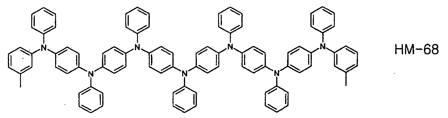
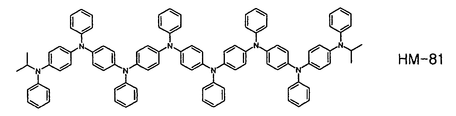
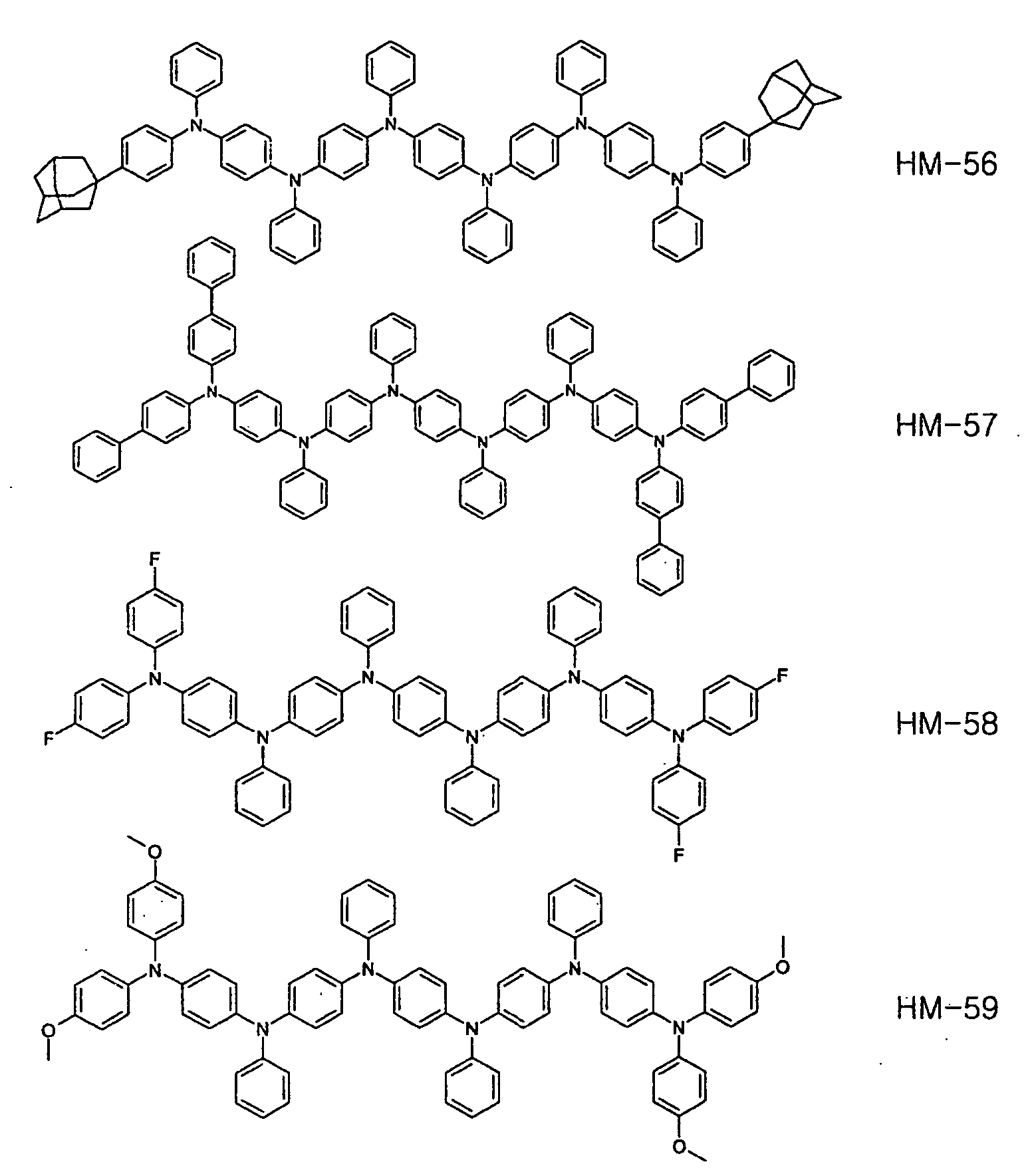
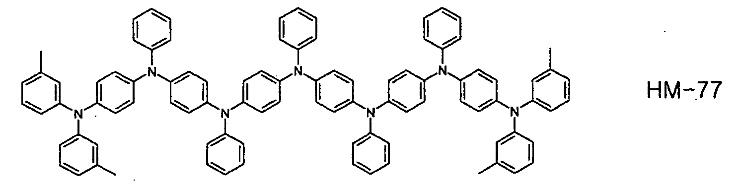
- the material for the hole injecting layer and the hole transport layer may be selected from any one of the following chemical formula 2, to which 'R1' and 'R2' are applied:
- one of the materials for the hole injecting layer and/or the hole transport layer, HM-32 will be synthesized as follows.
- diphenylamine 50g, 0.30mol
- dibromobenzene 104g, 0.44mol
- BINAP 2,2'-Bis(diphenylphosphino)-1,1'-binaphthyl
- Pd(OAc) 2 Palladium(II)acetate] (2.0g, 3%mol)
- NaO t Bu sodium tert-butoxide] (42.6g, 0.44mol)
- the flask having the resultant solution is cooled, and then toluene, a solvent of the reaction, is removed from the resultant solution.
- the resultant solution having no toluene reacts on methylene-chloride and water, and then methylene-chloride is removed therefrom, and is performed by silica gel column chromatography with a solvent of methylene-chloride and hexane at a ratio of 3 to 1.
- the resultant solution having no toluene reacts on methylene-chloride and water, and then methylene-chloride is removed therefrom, and is performed by silica gel column chromatography with a solvent of methylene-chloride and hexane at a ratio of 2 to 1. After that, the solvent is removed from the resultant solution of completing silica gel column chromatography, and is recrystallized and filtered with methylene-chloride and petroleum ether, thereby obtaining a white solid, N,N,N'-triphenyl-benzene-1,4-diamine (11.0g, 88%).
- N,N' -Diphenyl-1,4-phenylenediamine 5g, 0.019mol
- Dibromobenzene 45g, 0.19mol
- DPPf[1,1' -Bis(diphenylphosphino)ferrocene] (0.71g, 6% mol
- Pd(OAc) 2 2.0g, 4%mol
- NaO t Bu 7.0g, 0.07mol
- the flask having the resultant solution is cooled, and then toluene, a solvent of the reaction, is removed from the resultant solution.
- the resultant solution having no toluene is dissolved in methylene-chloride, and then is performed by silica gel column chromatography (methylene-chloride).
- the solvent is removed from the resultant solution performed by silica gel column chromatography, and is recrystallized and filtered by using methylene-chloride and methanol, thereby obtaining a gray solid, N,N'-bis(3-bromophenyl)-N,N'-diphenyl-1,4-phenylenediamine (6.5g, 60%).
- N,N,N'-triphenyl-benzene-1,4-diamine (2.54g, 0.0066mol), N,N' -Bis(3-bromophenyl)-N,N' -diphenyl-1,4-phenylenediamine (1.5g, 0.0026mol), BINAP (0.7g, 4%mol), Pd(OAc) 2 (0.02g, 3%mol), and NaO t Bu (17.2g, 0.0092mol) are dissolved in toluene (100mL), and then are maintained for 40 hours by reflux.
- the flask having the resultant solution is cooled, and then toluene, a solvent of the reaction, is removed from the resultant solution.
- the resultant solution having no toluene is filtered by methanol, and then is dissolved in chloro-benzene.
- the solution dissolved in chloro-benzene is performed by silica gel column chromatography, thereby removing impurities and solvent from the solution.
- the solution having no impurities and solvent is recrystallized and filter by using chloro-benzene and hexane, thereby obtaining a white solid, HM-32 (1.8g, 64%).
- an ITO glass substrate is patterned to have a luminescence area of 3mmX3mm
- the ITO glass substrate is cleaned.
- the ITO glass substrate is mounted in a vacuum chamber, and a base pressure is set at 1.0X10 -6 torr.
- an organic material is formed in order of HM-32(600 ⁇ ) / NPB(400 ⁇ ) / Alq 3 (C6)(200 ⁇ , 3%) /Alq3(400A) / LiF(5 ⁇ ) / Al(1000 ⁇ ).
- an ITO glass substrate is patterned to have a luminescence area of 3mmX3mm
- the ITO glass substrate is cleaned.
- the ITO glass substrate is mounted in a vacuum chamber, and a base pressure is set at 1.0X10 -6 torr.
- an organic material is formed in order of CuPC(200 ⁇ ) / HM-02(400A) / Alq 3 (C6)(200 ⁇ , 3%) /Alq3(400A) / LiF(5 ⁇ ) / Al(1000 ⁇ ).
- the related art embodiments of the organic electroluminescence device in which the hole injecting layer is formed of CuPC, will be described as follows.
- the organic electroluminescence device realizes the improvement of luminance, and decrease of the driving voltage.
- the hole injecting layer or the hole transport layer is formed of some materials having the structure of the chemical formula 1.
- the hole injecting layer or the hole transport layer is formed of the material having the chemical formula 3
- both the hole injecting layer and the hole transport layer may be formed of the material having the chemical formula 1, for the improvement of luminance and the decrease on driving voltage.
- the organic electroluminescence device according to the present invention has the following advantages.
- the hole injecting layer and the hole transport layer are formed of the material having the aforementioned chemical formula 1, so that it is possible to improve the luminance and to decrease the driving voltage, thereby increasing the life span of the device by improving the operation characteristics.
Landscapes
- Chemical & Material Sciences (AREA)
- Engineering & Computer Science (AREA)
- Materials Engineering (AREA)
- Organic Chemistry (AREA)
- Physics & Mathematics (AREA)
- Spectroscopy & Molecular Physics (AREA)
- Food Science & Technology (AREA)
- Electroluminescent Light Sources (AREA)
Abstract
Description


Claims (5)
- An organic electroluminescence device comprising:an anode, a hole injecting layer, a hole transport layer, an emitting layer, and a cathode, wherein, the hole injecting layer and the hole transport layer are formed of the material expressed by the following chemical formula 1:herein, 'n' is a positive number between 1 and 4, and 'R1' or 'R2' is selected from the group consisting of a substituted or non-substituted aromatic group, a hetero ring group, an aliphatic group, or hydrogen.

- The organic electroluminescence device as claimed in claim 1, wherein at least any one of 'R1' and 'R2' may be selected from substituted or non-substituted phenyl, biphenyl, pyridyl, naphthyl, quinolyl, isoquinolyl, fluorenyl, terphenyl, anthryl, phenanthryl, methyl, ethyl, propyl, isopropyl and the like.
- The organic electroluminescence device as claimed in claim 1, wherein a substituent on each of the substituted 'R1' and 'R2' may be selected from the group consisting of alkyl, aryl, alkoxyl, halogen, cyano, alkylaryl, vinylaryl and the like.
- The organic electroluminescence device as claimed in claim 3, wherein the substituent may be selected from the group consisting of methyl, ethyl, propyl, isopropyl, t-butyl, cyclohexyl, methoxy, ethoxy, propoxy, butoxy, fluoro, chloro, phenoxy, tolyloxy and the like.
- The organic electroluminescence device as claimed in claim 1, wherein the hole injecting layer and the hole transport layer are formed of any one material having the following chemical formula 2:


Applications Claiming Priority (2)
| Application Number | Priority Date | Filing Date | Title |
|---|---|---|---|
| KR1020040019356A KR100565665B1 (en) | 2004-03-22 | 2004-03-22 | organic electroluminescence device |
| KR2004019356 | 2004-03-22 |
Publications (3)
| Publication Number | Publication Date |
|---|---|
| EP1586616A2 true EP1586616A2 (en) | 2005-10-19 |
| EP1586616A3 EP1586616A3 (en) | 2007-07-04 |
| EP1586616B1 EP1586616B1 (en) | 2011-09-14 |
Family
ID=34934320
Family Applications (1)
| Application Number | Title | Priority Date | Filing Date |
|---|---|---|---|
| EP05005801A Active EP1586616B1 (en) | 2004-03-22 | 2005-03-17 | Organic electroluminescence device |
Country Status (6)
| Country | Link |
|---|---|
| US (1) | US7576484B2 (en) |
| EP (1) | EP1586616B1 (en) |
| JP (1) | JP4231491B2 (en) |
| KR (1) | KR100565665B1 (en) |
| CN (1) | CN100468822C (en) |
| AT (1) | ATE524841T1 (en) |
Cited By (4)
| Publication number | Priority date | Publication date | Assignee | Title |
|---|---|---|---|---|
| EP1979915A2 (en) * | 2005-12-28 | 2008-10-15 | E.I. Du Pont De Nemours And Company | Compositions comprising novel compounds and electronic devices made with such compositions |
| US8440324B2 (en) | 2005-12-27 | 2013-05-14 | E I Du Pont De Nemours And Company | Compositions comprising novel copolymers and electronic devices made with such compositions |
| US8617720B2 (en) | 2009-12-21 | 2013-12-31 | E I Du Pont De Nemours And Company | Electroactive composition and electronic device made with the composition |
| EP3053910A1 (en) * | 2013-10-04 | 2016-08-10 | Nissan Chemical Industries, Ltd. | Aniline derivatives and uses thereof |
Families Citing this family (13)
| Publication number | Priority date | Publication date | Assignee | Title |
|---|---|---|---|---|
| WO2006046441A1 (en) * | 2004-10-29 | 2006-05-04 | Idemitsu Kosan Co., Ltd. | Aromatic amine compound and organic electroluminescent device using same |
| US20060226429A1 (en) * | 2005-04-08 | 2006-10-12 | Sigalas Mihail M | Method and apparatus for directional organic light emitting diodes |
| JP2007077064A (en) * | 2005-09-14 | 2007-03-29 | Sony Corp | Arylamine compound, method for synthesizing the same and organic electroluminescent element |
| CN104789111B (en) * | 2007-04-12 | 2018-05-01 | 日产化学工业株式会社 | Oligoaniline compound |
| JP5205859B2 (en) * | 2007-08-09 | 2013-06-05 | 東ソー株式会社 | Novel benzo [c] fluorene derivatives and uses thereof |
| EP2491003A4 (en) | 2009-10-19 | 2015-06-03 | Du Pont | Triarylamine compounds for electronic applications |
| KR20120086319A (en) | 2009-10-19 | 2012-08-02 | 이 아이 듀폰 디 네모아 앤드 캄파니 | Triarylamine compounds for electronic applications |
| WO2014185535A1 (en) | 2013-05-16 | 2014-11-20 | ダイキン工業株式会社 | Fullerene derivative and n-type semiconductor material |
| US10164196B2 (en) | 2013-06-21 | 2018-12-25 | Nissan Chemical Industries, Ltd. | Aniline derivative, charge-transporting varnish and organic electroluminescent device |
| US10147885B2 (en) * | 2015-02-24 | 2018-12-04 | Nissan Chemical Industries, Ltd. | Aniline derivatives and uses thereof |
| WO2017116168A1 (en) * | 2015-12-31 | 2017-07-06 | 머티어리얼사이언스 주식회사 | Organic electroluminescent element |
| CN110183333B (en) | 2019-06-19 | 2020-06-30 | 陕西莱特光电材料股份有限公司 | Organic electroluminescent material and organic electroluminescent device containing same |
| CN110563647B (en) * | 2019-08-27 | 2021-02-12 | 陕西莱特光电材料股份有限公司 | Nitrogen-containing compound, organic electroluminescent device, and photoelectric conversion device |
Family Cites Families (9)
| Publication number | Priority date | Publication date | Assignee | Title |
|---|---|---|---|---|
| JP3296147B2 (en) * | 1994-08-04 | 2002-06-24 | 東洋インキ製造株式会社 | Triphenylamine polymer, its production method and use |
| JP3758694B2 (en) * | 1994-10-13 | 2006-03-22 | 三星エスディアイ株式会社 | Organic thin film EL device |
| JPH09151371A (en) * | 1995-11-30 | 1997-06-10 | Toppan Printing Co Ltd | Organic thin film el element |
| JP4013282B2 (en) | 1997-05-09 | 2007-11-28 | コニカミノルタホールディングス株式会社 | Electroluminescent device |
| JPH11251068A (en) | 1998-02-27 | 1999-09-17 | Asahi Glass Co Ltd | Organic electroluminescence element |
| JP3735703B2 (en) | 1999-12-21 | 2006-01-18 | 大阪大学長 | Electroluminescence element |
| EP1496044B1 (en) * | 2002-03-27 | 2010-11-03 | Bando Chemical Industries, Ltd. | Novel 1,3,5-tris(arylamino)benzene |
| KR101014837B1 (en) | 2002-08-09 | 2011-02-15 | 도소 가부시키가이샤 | Novel triarylamine polymer, process for producing the same, and use thereof |
| TWI280973B (en) * | 2002-08-28 | 2007-05-11 | Sumitomo Chemical Co | Polymer compound and polymer light-emitting device using the same |
-
2004
- 2004-03-22 KR KR1020040019356A patent/KR100565665B1/en active IP Right Grant
-
2005
- 2005-03-17 AT AT05005801T patent/ATE524841T1/en not_active IP Right Cessation
- 2005-03-17 EP EP05005801A patent/EP1586616B1/en active Active
- 2005-03-21 US US11/084,021 patent/US7576484B2/en active Active
- 2005-03-22 CN CNB2005100564575A patent/CN100468822C/en active Active
- 2005-03-22 JP JP2005081539A patent/JP4231491B2/en active Active
Non-Patent Citations (1)
| Title |
|---|
| None |
Cited By (6)
| Publication number | Priority date | Publication date | Assignee | Title |
|---|---|---|---|---|
| US8440324B2 (en) | 2005-12-27 | 2013-05-14 | E I Du Pont De Nemours And Company | Compositions comprising novel copolymers and electronic devices made with such compositions |
| EP1979915A2 (en) * | 2005-12-28 | 2008-10-15 | E.I. Du Pont De Nemours And Company | Compositions comprising novel compounds and electronic devices made with such compositions |
| EP1979915A4 (en) * | 2005-12-28 | 2009-08-05 | Du Pont | Compositions comprising novel compounds and electronic devices made with such compositions |
| US8617720B2 (en) | 2009-12-21 | 2013-12-31 | E I Du Pont De Nemours And Company | Electroactive composition and electronic device made with the composition |
| EP3053910A1 (en) * | 2013-10-04 | 2016-08-10 | Nissan Chemical Industries, Ltd. | Aniline derivatives and uses thereof |
| EP3053910A4 (en) * | 2013-10-04 | 2017-05-17 | Nissan Chemical Industries, Ltd. | Aniline derivatives and uses thereof |
Also Published As
| Publication number | Publication date |
|---|---|
| JP4231491B2 (en) | 2009-02-25 |
| CN1674747A (en) | 2005-09-28 |
| CN100468822C (en) | 2009-03-11 |
| KR100565665B1 (en) | 2006-03-30 |
| JP2005276832A (en) | 2005-10-06 |
| US20050208334A1 (en) | 2005-09-22 |
| KR20050094195A (en) | 2005-09-27 |
| EP1586616A3 (en) | 2007-07-04 |
| EP1586616B1 (en) | 2011-09-14 |
| ATE524841T1 (en) | 2011-09-15 |
| US7576484B2 (en) | 2009-08-18 |
Similar Documents
| Publication | Publication Date | Title |
|---|---|---|
| EP1586616B1 (en) | Organic electroluminescence device | |
| JP4129558B2 (en) | Organic EL display | |
| KR100577262B1 (en) | organic electroluminescence device | |
| KR101326668B1 (en) | Electron transporting-injection material and Organic electroluminescent device using the same | |
| WO2004075603A2 (en) | Organic electroluminescent device | |
| KR101914338B1 (en) | Novel organic compound and materials for organic electroluminescent devices comprising the same and organic electroluminescent devices comprising the same and | |
| KR101334204B1 (en) | A New Pyrene Compounds, Method of Producing the Same and Organic Electroluminescent Device Comprising the Same | |
| KR20130121516A (en) | Using new alylamine as hole transporting mateial and organic electroluminescent device using the same | |
| KR20120056418A (en) | Electron transporting material and Organic electroluminescent display device using the same | |
| KR100525409B1 (en) | organic electroluminescence device | |
| KR20110005516A (en) | Blue color fluorescent material and organic electroluminescent device using the same | |
| KR101375542B1 (en) | Hole transporting material comprising thiophen derivative and organic electroluminescent device using the same | |
| KR100793795B1 (en) | Organic electroluminescence devices | |
| KR20090072152A (en) | Pyrene derivatives and organic electroluminescent devices employing the same | |
| KR101327301B1 (en) | Amine derivative as hole transporting material and organic electroluminescent device using the same | |
| KR100887870B1 (en) | New anthracene derivatives, preparation method thereof and organic electronic device using the same | |
| KR100525415B1 (en) | organic electroluminescence device | |
| KR101561554B1 (en) | - Electron transporting-injection material and Organic electroluminescent device using the same | |
| KR20060118913A (en) | Organic electroluminescence device | |
| KR20060117038A (en) | Light emitting compound and oled | |
| KR20120038818A (en) | Red color phosphorescent host material and organic electroluminescent display device using the same | |
| KR20120056000A (en) | Electron transporting material and Organic electroluminescent display device using the same | |
| KR100379442B1 (en) | organic electroluminescence device | |
| KR20040085681A (en) | organic electroluminescence device | |
| KR20130043342A (en) | Blue phosphorescent compound and organic electroluminescent device using the same |
Legal Events
| Date | Code | Title | Description |
|---|---|---|---|
| PUAI | Public reference made under article 153(3) epc to a published international application that has entered the european phase |
Free format text: ORIGINAL CODE: 0009012 |
|
| 17P | Request for examination filed |
Effective date: 20050317 |
|
| AK | Designated contracting states |
Kind code of ref document: A2 Designated state(s): AT BE BG CH CY CZ DE DK EE ES FI FR GB GR HU IE IS IT LI LT LU MC NL PL PT RO SE SI SK TR |
|
| AX | Request for extension of the european patent |
Extension state: AL BA HR LV MK YU |
|
| PUAL | Search report despatched |
Free format text: ORIGINAL CODE: 0009013 |
|
| AK | Designated contracting states |
Kind code of ref document: A3 Designated state(s): AT BE BG CH CY CZ DE DK EE ES FI FR GB GR HU IE IS IT LI LT LU MC NL PL PT RO SE SI SK TR |
|
| AX | Request for extension of the european patent |
Extension state: AL BA HR LV MK YU |
|
| RIC1 | Information provided on ipc code assigned before grant |
Ipc: C07C 211/54 20060101ALI20070525BHEP Ipc: H01L 51/00 20060101AFI20070525BHEP |
|
| 17Q | First examination report despatched |
Effective date: 20080128 |
|
| AKX | Designation fees paid |
Designated state(s): AT BE BG CH CY CZ DE DK EE ES FI FR GB GR HU IE IS IT LI LT LU MC NL PL PT RO SE SI SK TR |
|
| RAP1 | Party data changed (applicant data changed or rights of an application transferred) |
Owner name: LG DISPLAY CO., LTD. |
|
| REG | Reference to a national code |
Ref country code: DE Ref legal event code: R079 Ref document number: 602005029968 Country of ref document: DE Free format text: PREVIOUS MAIN CLASS: C09K0011060000 Ipc: H01L0051540000 |
|
| GRAP | Despatch of communication of intention to grant a patent |
Free format text: ORIGINAL CODE: EPIDOSNIGR1 |
|
| RIC1 | Information provided on ipc code assigned before grant |
Ipc: C07C 211/54 20060101ALI20110224BHEP Ipc: H01L 51/54 20060101AFI20110224BHEP |
|
| GRAS | Grant fee paid |
Free format text: ORIGINAL CODE: EPIDOSNIGR3 |
|
| GRAA | (expected) grant |
Free format text: ORIGINAL CODE: 0009210 |
|
| AK | Designated contracting states |
Kind code of ref document: B1 Designated state(s): AT BE BG CH CY CZ DE DK EE ES FI FR GB GR HU IE IS IT LI LT LU MC NL PL PT RO SE SI SK TR |
|
| REG | Reference to a national code |
Ref country code: GB Ref legal event code: FG4D |
|
| REG | Reference to a national code |
Ref country code: CH Ref legal event code: EP |
|
| REG | Reference to a national code |
Ref country code: IE Ref legal event code: FG4D Ref country code: DE Ref legal event code: R082 Ref document number: 602005029968 Country of ref document: DE Representative=s name: TER MEER STEINMEISTER & PARTNER GBR PATENTANWA, DE Ref country code: DE Ref legal event code: R082 Ref document number: 602005029968 Country of ref document: DE Representative=s name: TER MEER STEINMEISTER & PARTNER PATENTANWAELTE, DE |
|
| REG | Reference to a national code |
Ref country code: DE Ref legal event code: R096 Ref document number: 602005029968 Country of ref document: DE Effective date: 20111201 |
|
| REG | Reference to a national code |
Ref country code: NL Ref legal event code: VDEP Effective date: 20110914 |
|
| PG25 | Lapsed in a contracting state [announced via postgrant information from national office to epo] |
Ref country code: SE Free format text: LAPSE BECAUSE OF FAILURE TO SUBMIT A TRANSLATION OF THE DESCRIPTION OR TO PAY THE FEE WITHIN THE PRESCRIBED TIME-LIMIT Effective date: 20110914 Ref country code: LT Free format text: LAPSE BECAUSE OF FAILURE TO SUBMIT A TRANSLATION OF THE DESCRIPTION OR TO PAY THE FEE WITHIN THE PRESCRIBED TIME-LIMIT Effective date: 20110914 Ref country code: FI Free format text: LAPSE BECAUSE OF FAILURE TO SUBMIT A TRANSLATION OF THE DESCRIPTION OR TO PAY THE FEE WITHIN THE PRESCRIBED TIME-LIMIT Effective date: 20110914 |
|
| LTIE | Lt: invalidation of european patent or patent extension |
Effective date: 20110914 |
|
| PG25 | Lapsed in a contracting state [announced via postgrant information from national office to epo] |
Ref country code: SI Free format text: LAPSE BECAUSE OF FAILURE TO SUBMIT A TRANSLATION OF THE DESCRIPTION OR TO PAY THE FEE WITHIN THE PRESCRIBED TIME-LIMIT Effective date: 20110914 Ref country code: GR Free format text: LAPSE BECAUSE OF FAILURE TO SUBMIT A TRANSLATION OF THE DESCRIPTION OR TO PAY THE FEE WITHIN THE PRESCRIBED TIME-LIMIT Effective date: 20111215 Ref country code: AT Free format text: LAPSE BECAUSE OF FAILURE TO SUBMIT A TRANSLATION OF THE DESCRIPTION OR TO PAY THE FEE WITHIN THE PRESCRIBED TIME-LIMIT Effective date: 20110914 Ref country code: CY Free format text: LAPSE BECAUSE OF FAILURE TO SUBMIT A TRANSLATION OF THE DESCRIPTION OR TO PAY THE FEE WITHIN THE PRESCRIBED TIME-LIMIT Effective date: 20110914 |
|
| REG | Reference to a national code |
Ref country code: AT Ref legal event code: MK05 Ref document number: 524841 Country of ref document: AT Kind code of ref document: T Effective date: 20110914 |
|
| PG25 | Lapsed in a contracting state [announced via postgrant information from national office to epo] |
Ref country code: BE Free format text: LAPSE BECAUSE OF FAILURE TO SUBMIT A TRANSLATION OF THE DESCRIPTION OR TO PAY THE FEE WITHIN THE PRESCRIBED TIME-LIMIT Effective date: 20110914 |
|
| PG25 | Lapsed in a contracting state [announced via postgrant information from national office to epo] |
Ref country code: IS Free format text: LAPSE BECAUSE OF FAILURE TO SUBMIT A TRANSLATION OF THE DESCRIPTION OR TO PAY THE FEE WITHIN THE PRESCRIBED TIME-LIMIT Effective date: 20120114 Ref country code: SK Free format text: LAPSE BECAUSE OF FAILURE TO SUBMIT A TRANSLATION OF THE DESCRIPTION OR TO PAY THE FEE WITHIN THE PRESCRIBED TIME-LIMIT Effective date: 20110914 Ref country code: CZ Free format text: LAPSE BECAUSE OF FAILURE TO SUBMIT A TRANSLATION OF THE DESCRIPTION OR TO PAY THE FEE WITHIN THE PRESCRIBED TIME-LIMIT Effective date: 20110914 |
|
| PG25 | Lapsed in a contracting state [announced via postgrant information from national office to epo] |
Ref country code: IT Free format text: LAPSE BECAUSE OF FAILURE TO SUBMIT A TRANSLATION OF THE DESCRIPTION OR TO PAY THE FEE WITHIN THE PRESCRIBED TIME-LIMIT Effective date: 20110914 Ref country code: NL Free format text: LAPSE BECAUSE OF FAILURE TO SUBMIT A TRANSLATION OF THE DESCRIPTION OR TO PAY THE FEE WITHIN THE PRESCRIBED TIME-LIMIT Effective date: 20110914 Ref country code: PL Free format text: LAPSE BECAUSE OF FAILURE TO SUBMIT A TRANSLATION OF THE DESCRIPTION OR TO PAY THE FEE WITHIN THE PRESCRIBED TIME-LIMIT Effective date: 20110914 Ref country code: PT Free format text: LAPSE BECAUSE OF FAILURE TO SUBMIT A TRANSLATION OF THE DESCRIPTION OR TO PAY THE FEE WITHIN THE PRESCRIBED TIME-LIMIT Effective date: 20120116 Ref country code: RO Free format text: LAPSE BECAUSE OF FAILURE TO SUBMIT A TRANSLATION OF THE DESCRIPTION OR TO PAY THE FEE WITHIN THE PRESCRIBED TIME-LIMIT Effective date: 20110914 Ref country code: EE Free format text: LAPSE BECAUSE OF FAILURE TO SUBMIT A TRANSLATION OF THE DESCRIPTION OR TO PAY THE FEE WITHIN THE PRESCRIBED TIME-LIMIT Effective date: 20110914 |
|
| PLBE | No opposition filed within time limit |
Free format text: ORIGINAL CODE: 0009261 |
|
| STAA | Information on the status of an ep patent application or granted ep patent |
Free format text: STATUS: NO OPPOSITION FILED WITHIN TIME LIMIT |
|
| PG25 | Lapsed in a contracting state [announced via postgrant information from national office to epo] |
Ref country code: DK Free format text: LAPSE BECAUSE OF FAILURE TO SUBMIT A TRANSLATION OF THE DESCRIPTION OR TO PAY THE FEE WITHIN THE PRESCRIBED TIME-LIMIT Effective date: 20110914 |
|
| 26N | No opposition filed |
Effective date: 20120615 |
|
| REG | Reference to a national code |
Ref country code: DE Ref legal event code: R097 Ref document number: 602005029968 Country of ref document: DE Effective date: 20120615 |
|
| PG25 | Lapsed in a contracting state [announced via postgrant information from national office to epo] |
Ref country code: MC Free format text: LAPSE BECAUSE OF NON-PAYMENT OF DUE FEES Effective date: 20120331 |
|
| REG | Reference to a national code |
Ref country code: CH Ref legal event code: PL |
|
| REG | Reference to a national code |
Ref country code: IE Ref legal event code: MM4A |
|
| PG25 | Lapsed in a contracting state [announced via postgrant information from national office to epo] |
Ref country code: CH Free format text: LAPSE BECAUSE OF NON-PAYMENT OF DUE FEES Effective date: 20120331 Ref country code: IE Free format text: LAPSE BECAUSE OF NON-PAYMENT OF DUE FEES Effective date: 20120317 Ref country code: LI Free format text: LAPSE BECAUSE OF NON-PAYMENT OF DUE FEES Effective date: 20120331 |
|
| PG25 | Lapsed in a contracting state [announced via postgrant information from national office to epo] |
Ref country code: ES Free format text: LAPSE BECAUSE OF FAILURE TO SUBMIT A TRANSLATION OF THE DESCRIPTION OR TO PAY THE FEE WITHIN THE PRESCRIBED TIME-LIMIT Effective date: 20111225 |
|
| PG25 | Lapsed in a contracting state [announced via postgrant information from national office to epo] |
Ref country code: BG Free format text: LAPSE BECAUSE OF FAILURE TO SUBMIT A TRANSLATION OF THE DESCRIPTION OR TO PAY THE FEE WITHIN THE PRESCRIBED TIME-LIMIT Effective date: 20111214 |
|
| PG25 | Lapsed in a contracting state [announced via postgrant information from national office to epo] |
Ref country code: TR Free format text: LAPSE BECAUSE OF FAILURE TO SUBMIT A TRANSLATION OF THE DESCRIPTION OR TO PAY THE FEE WITHIN THE PRESCRIBED TIME-LIMIT Effective date: 20110914 |
|
| PG25 | Lapsed in a contracting state [announced via postgrant information from national office to epo] |
Ref country code: LU Free format text: LAPSE BECAUSE OF NON-PAYMENT OF DUE FEES Effective date: 20120317 |
|
| PG25 | Lapsed in a contracting state [announced via postgrant information from national office to epo] |
Ref country code: HU Free format text: LAPSE BECAUSE OF FAILURE TO SUBMIT A TRANSLATION OF THE DESCRIPTION OR TO PAY THE FEE WITHIN THE PRESCRIBED TIME-LIMIT Effective date: 20050317 |
|
| REG | Reference to a national code |
Ref country code: FR Ref legal event code: PLFP Year of fee payment: 12 |
|
| REG | Reference to a national code |
Ref country code: FR Ref legal event code: PLFP Year of fee payment: 13 |
|
| REG | Reference to a national code |
Ref country code: FR Ref legal event code: PLFP Year of fee payment: 14 |
|
| REG | Reference to a national code |
Ref country code: DE Ref legal event code: R079 Ref document number: 602005029968 Country of ref document: DE Free format text: PREVIOUS MAIN CLASS: H01L0051540000 Ipc: H10K0085000000 |
|
| PGFP | Annual fee paid to national office [announced via postgrant information from national office to epo] |
Ref country code: DE Payment date: 20240122 Year of fee payment: 20 Ref country code: GB Payment date: 20240122 Year of fee payment: 20 |
|
| PGFP | Annual fee paid to national office [announced via postgrant information from national office to epo] |
Ref country code: FR Payment date: 20240123 Year of fee payment: 20 |