EP1586111B1 - Wirebonding method and apparatus - Google Patents
Wirebonding method and apparatus Download PDFInfo
- Publication number
- EP1586111B1 EP1586111B1 EP20030813211 EP03813211A EP1586111B1 EP 1586111 B1 EP1586111 B1 EP 1586111B1 EP 20030813211 EP20030813211 EP 20030813211 EP 03813211 A EP03813211 A EP 03813211A EP 1586111 B1 EP1586111 B1 EP 1586111B1
- Authority
- EP
- European Patent Office
- Prior art keywords
- wirebonding
- clamp
- row
- lead frames
- lead
- Prior art date
- Legal status (The legal status is an assumption and is not a legal conclusion. Google has not performed a legal analysis and makes no representation as to the accuracy of the status listed.)
- Expired - Lifetime
Links
Images


Classifications
-
- H—ELECTRICITY
- H10—SEMICONDUCTOR DEVICES; ELECTRIC SOLID-STATE DEVICES NOT OTHERWISE PROVIDED FOR
- H10W—GENERIC PACKAGES, INTERCONNECTIONS, CONNECTORS OR OTHER CONSTRUCTIONAL DETAILS OF DEVICES COVERED BY CLASS H10
- H10W72/00—Interconnections or connectors in packages
- H10W72/071—Connecting or disconnecting
- H10W72/075—Connecting or disconnecting of bond wires
-
- H—ELECTRICITY
- H10—SEMICONDUCTOR DEVICES; ELECTRIC SOLID-STATE DEVICES NOT OTHERWISE PROVIDED FOR
- H10W—GENERIC PACKAGES, INTERCONNECTIONS, CONNECTORS OR OTHER CONSTRUCTIONAL DETAILS OF DEVICES COVERED BY CLASS H10
- H10W72/00—Interconnections or connectors in packages
- H10W72/071—Connecting or disconnecting
- H10W72/0711—Apparatus therefor
- H10W72/07141—Means for applying energy, e.g. ovens or lasers
-
- H—ELECTRICITY
- H10—SEMICONDUCTOR DEVICES; ELECTRIC SOLID-STATE DEVICES NOT OTHERWISE PROVIDED FOR
- H10W—GENERIC PACKAGES, INTERCONNECTIONS, CONNECTORS OR OTHER CONSTRUCTIONAL DETAILS OF DEVICES COVERED BY CLASS H10
- H10W72/00—Interconnections or connectors in packages
- H10W72/50—Bond wires
- H10W72/551—Materials of bond wires
- H10W72/552—Materials of bond wires comprising metals or metalloids, e.g. silver
Definitions
- the present invention relates to a method and apparatus for wirebonding leads of a plurality of lead frames being part of a lead frame assembly by a wirebonding tool to semiconductor products mounted on the respective lead frames, the lead frame assembly being indexable in an index direction relative to a wirebonding frame, a first clamp and a second clamp clamping the leads of adjacent lead frames during wirebonding.
- a leadframe assembly may be an endless strip or a strip or film having a discrete length. Each of said strips or film comprises at least two parallel rows of lead frames.
- IC Integrated Circuit
- chips are prepared. These semiconductor products are to be accommodated in a package and need to be electrically connectable to components outside the package.
- a plurality of semiconductor products is first mounted on lead frames in a so-called die bonding process.
- each semiconductor product is electrically connected to the associated lead frame in a so-called wirebonding process before packaging the semiconductor product.
- wirebonding process bond pads on one or more surfaces of each semiconductor product are electrically and mechanically connected to leads of the associated lead frame by thin metallic wires, using a wirebonding tool.
- the process of wirebonding one semiconductor product on a lead frame generally requires several steps including, in a working area of a wirebonding apparatus, positioning the lead frame relative to a clamping mechanism, operating different clamping elements, operating the wirebonding tool(s), and indexing the lead frame for bringing a new semiconductor product and associated leads of the lead frame into the working area of the wirebonding apparatus.
- US Patent no. 6,068,174 discloses a wirebonding apparatus including a heat block or other base member for supporting a lead frame during wirebonding. Separate sets of leads of the lead frame associated with a particular semiconductor product are fixedly held against the heat block by different clamping elements of a clamping mechanism, whereby separate sets of leads are wire bonded by a wirebonding tool at different times.
- a relative long lead frame indexing time, or many indexing operations for a lead frame, will lead to a relative low throughput of the wirebonding apparatus. Consequently, a reduction of the lead frame indexing time in which the bonding tool must be inoperative will lead to an increase in the throughput of the wirebonding apparatus.
- US Patent no. 5,322,207 discloses an automated wirebonding apparatus wherein a single indexing step for the lead frame enables two or more semiconductor products to be wirebonded, before a next lead frame indexing step is to be taken, which results in a decrease of the overall time for wirebonding all semiconductor products on the lead frame, and thus in a decrease of the mean wirebonding cycle time per semiconductor product.
- EP0542465 discloses an indexing work holder for an automatic bonding machine having an indexing head with a gripper mechanism for gripping a lead frame and with means for rotating the lead frame into a predetermined theta orientation after being gripped and before bonding.
- the jaws of the gripper mechanism may have pivoted inserts and the orienting means may comprise a linear actuator coupled to a theta bar.
- D2: US6334566 discloses a wire-bonding machine including a heat block for supporting a lead frame during wire-bonding.
- a clamp mechanism in the machine clamps leads of the lead frame during wire-bonding by fixedly holding sets of the leads against the heat block one set at a time.
- a wire-bonding tool wire-bonds leads clamped by the clamp mechanism to bond pads on an integrated circuit die.
- first clamp and the second clamp each comprise a clamping frame being movable towards and away from the semiconductor product on the associated lead frame, and a base member being movable towards and away from the lead frame at the side facing away from the semiconductor product.
- the steps (a)-(g) are not performed in succession, i.e. in general a next step will not be taken only when the previous step is completed. Some steps may be taken in parallel, as will be explained hereafter.
- the clamping of the second clamp according to step (b) may be initiated concurrently with the initiation of the clamping of the first clamp according to step (a), but may also be later in time.
- the initiation of the clamping of the second clamp will be at any moment during the clamping time of the first clamp, before the first clamp is released.
- the first clamp may be released immediately after completing step (a), i.e. after completing the wirebonding of the leads of the n-th lead frame of the n lead frames clamped by the first clamp, but this release may also be later in time, during the clamping time of the second clamp.
- the release of the first clamp should be completed before step (d) is initiated.
- the leads of n adjacent lead frames of the second row of lead frames is still are still clamped by the second clamp to the second base member.
- the wirebonding of the leads of the n lead frames of the second row of lead frames by the wirebonding tool according to step (b) is continued during the indexing step (d), resulting in the indexing not interrupting the wirebonding, thus decreasing the mean semiconductor wirebonding cycle time.
- the second clamp may be released immediately after completing step (b), i.e. after completing the wirebonding of the leads of the n-th lead frame of the n lead frames clamped by the second clamp, but this release may also be later in time, e.g. during the clamping time of the first clamp.
- Step (f) Moving the second clamp back to its previous position relative to the wirebonding frame according to step (f) can only be performed after step (e) is completed. Step (f) should be completed before, in a repetition of steps (a)-(f), step (b) is performed again.
- step (a) can be initiated as soon as steps (b) and (d) are completed.
- the number n is 2 for an optimum path with the shortest route of the wirebonding tool across the lead frames of the first row and the second row.
- the number n may also be greater than 2, although this would result in at least one longer part of the path of the wirebonding tool when moving from the last lead frame of the first row to the first lead frame of the second row or vice versa.
- the n lead frames of the first row lead one lead frame pitch relative to the n lead frames of the second row, as seen in the index direction.
- the shortest paths for the wirebonding tool across the lead frame assembly are achieved.
- the first clamp in step (a) preferably further clamps n lead frames of the further row adjacent the n lead frames of the first row.
- the second clamp in step (b) preferably further clamps n lead frames of the further row adjacent the n lead frames of the second row.
- an optimum meandering wirebonding path can be followed by the wirebonding tool across the lead frames of the first and further row(s), and the lead frames of the second and further row(s), clamped by the first and second clamp, respectively.
- the first clamp is stationary relative to the wirebonding frame, as seen in the index direction.
- a wirebonding apparatus for wirebonding leads of a plurality of lead frames being part of a lead frame assembly to semiconductor products mounted on the respective lead frames, comprises: a wirebonding frame; an indexing device for indexing the lead frame assembly in an index direction relative to the wirebonding frame; at least a first clamp for clamping the leads of n (n ⁇ 1) adjacent lead frames of a first row of lead frames as seen in the index direction, the first clamp being stationary in the index direction relative to the wirebonding frame; at least a second clamp for clamping the leads of n adjacent lead frames of a second row of lead frames adjacent the first row, the second clamp being movable in the index direction relative to the wirebonding frame; and a wirebonding tool for wirebonding the leads of the n lead frames of the first and the second row to the corresponding semiconductor products, the wirebonding tool and the second clamp being adapted for following the index movement of the lead frame assembly.
- the wirebonding tool is preferably adapted to perform a wirebonding operation during the movement of the movement of
- first clamp and the second clamp are situated generally opposite to each other, as seen transversely to the index direction.
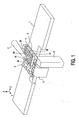
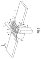
- Figs. 1-6 in a perspective view schematically illustrate consecutive steps in a wire-bonding operation.
- FIGs. 1-6 show a wirebonding frame 1 being part of a wire bonding apparatus (not shown in further detail).
- a lead frame assembly 2 of which only a part is shown in the Figures, comprises several rows (four rows, as seen in the X direction, in the example shown) of lead frames (not shown in detail) carrying semiconductor products 3 which are mounted in a regular arrangement. As seen in each row of semiconductor products 3, the (centre-to-centre) distance between adjacent semiconductor products 3 is indicated with "pitch".
- the lead frame assembly 2 may be of an arbitrary design, comprising leads (not shown in detail) in a configuration suitable for a particular semiconductor package.
- the semiconductor products 3 are provided with bond pads (not shown in detail) which are to be connected to the leads of the lead frames of the lead frame assembly 2 by wirebonding as known in the art.
- the wirebonding apparatus includes a clamping mechanism comprising a stationary clamp 4 extending over part of the area of the lead frame assembly 2 so as to clamp leads associated with at least two adjacent semiconductor products 3 in a row in one or more adjacent rows against a heat block or other base member (not shown).
- the stationary clamp 4 is adapted to clamp two adjacent semiconductor products 3 in three adjacent rows, i.e. a total of six semiconductor products 2, by means of suitable clamping elements (not shown).
- suitable clamping elements may take any suitable shape, e.g. fingers, brackets, or blocks.
- stationary clamp 4 is not movable in the indicated X and Y direction with respect to the wirebonding frame 1 of the wirebonding apparatus on which the stationary clamp 4 is mounted.
- at least part of the stationary clamp 4 comprising the clamping elements is movable in the Z direction between a first end position in which the leads of the lead frames under the stationary clamp 4 are clamped against said heat block or other base member, and a second end position in which the leads of the lead frames under the stationary clamp 4 are not clamped, providing the opportunity to move the lead frame assembly 2 in the X direction relative to the stationary clamp 4.
- the clamping mechanism of the wirebonding apparatus further comprises a movable clamp 5 extending over part of the area of the lead frame assembly 2 so as to clamp leads associated with at least two adjacent semiconductor products 3 in a row in one or more adjacent rows against a heat block or other base member.
- the movable clamp 5 is adapted to clamp two adjacent semiconductor products 3 in one row, i.e. a total of two semiconductor products 3, by means of suitable clamping elements.
- the adjective "movable” is used here to indicate that the movable clamp 5 is movable in the indicated X direction with respect to the wirebonding frame 1 of the wirebonding apparatus on which the movable clamp 5 is mounted.
- the movable clamp 5 comprising the clamping elements is movable in the Z direction between a first end position in which the leads of the lead frames under the movable clamp 5 are clamped against a heat block or other base member, and a second end position in which the leads of the lead frames under the movable clamp 5 are not clamped, providing the opportunity to move the lead frame assembly 2 in the X direction relative to the movable clamp 5.
- the stationary clamp 4 and the movable clamp 5 are situated generally opposite to each other, at opposite sides of the lead frame assembly 2.
- the movable clamp 5 is coupled to an index mechanism 6 such that with a displacement of the lead frame assembly 2 by the index mechanism 6 over a predetermined distance in the X direction also the movable clamp 5 moves over the same distance in the X direction.
- At least one bonding head 7 having a drive mechanism (not shown) is operable.
- semiconductor products 21, 22, 23, 24, 25, and 26 are clamped by the stationary clamp 4 in its first end position, and the semiconductor products 21-26 are wirebonded consecutively, as indicated in Figs. 1 and 2 illustrating the wirebonding of the first one and the last one of the semiconductor products 21-26, respectively.
- the stationary clamp 4 releases the lead frame assembly 2 by moving in the Z direction to its second end position.
- the semiconductor products 27, and 28 are clamped with the movable clamp 5 in its first end position.
- the index mechanism 6 then indexes the lead frame assembly 2 over twice the pitch of the semiconductor products 3 in the X direction.
- the movable clamp 5 and the wirebonding tool 7 follow the indexing movement of the indexing mechanism 6 by a suitable mechanical or electrical coupling therebetween, in particular between their respective (servo) drive motors. Meanwhile, the semiconductor products 27 and 28 are wirebonded.
- the movable clamp 5 releases the lead frame assembly 2 by moving in the Z direction to its second end position.
- the index mechanism 6 then moves back to its former position relative to the wirebonding frame 1 of the wirebonding apparatus, taking the movable clamp 5 along, but without displacing the lead frame assembly 2.
- the movable clamp 5 then clamps leads and semiconductor product 35 and an adjacent semiconductor product not shown in Fig. 6 by moving in the Z direction to its first end position, after which the clamped semiconductor products can be wirebonded.
- the lead frame assembly comprises only two rows of lead frames carrying semiconductor products e.g. a row comprising semiconductor products 26, 29 and 34, and a row comprising semiconductor products 27, 28, and 35.
- both the stationary clamp and the movable clamp are adapted to clamp only one semiconductor product at the time.
- the operational order of wirebonding would be semiconductor products 26, 27, 29, 28, 34, 35, etc., where the movable clamp would follow an indexing of the lead frame assembly over one pitch of the semiconductor products during the wirebonding of semiconductor products 27, 28, 35, etc.
- the lead frame assembly comprises only two rows of lead frames carrying semiconductor products e.g. a row comprising semiconductor products 26, 29 and 34, and a row comprising semiconductor products 27, 28, and 35. If both the stationary clamp and the moving clamp would be adapted to clamp two adjacent semiconductor products in a row at the time, the operational wirebonding order would be semiconductor products 21, 26, 27, 28, 29, 34, 35, etc., where the movable clamp would follow an indexing of the lead frame assembly over two pitches of the semiconductor products during the wirebonding of at least one of semiconductor products 27, 28, 35, etc.
- a meandering wirebonding path may followed over and across the lead frame assembly 2 by the wirebonding tool 7 for a minimum bonding time to be realized.
- other paths may be followed as well.
- the indexing of the lead frame assembly 2 is performed during the wirebonding process, which thus does not need to be interrupted for the indexing.
- More than one bonding tool 7 may be employed.
- a wirebonding method and apparatus have been disclosed in which the lead frame assembly indexing time is virtually taken out of the critical time path of the wirebonding process by using a clamping mechanism comprising a stationary clamp and a movable clamp.
Landscapes
- Wire Bonding (AREA)
- Superconductors And Manufacturing Methods Therefor (AREA)
- Crystals, And After-Treatments Of Crystals (AREA)
- Analysing Materials By The Use Of Radiation (AREA)
Abstract
Description
- The present invention relates to a method and apparatus for wirebonding leads of a plurality of lead frames being part of a lead frame assembly by a wirebonding tool to semiconductor products mounted on the respective lead frames, the lead frame assembly being indexable in an index direction relative to a wirebonding frame, a first clamp and a second clamp clamping the leads of adjacent lead frames during wirebonding. Within the scope of this invention, a leadframe assembly may be an endless strip or a strip or film having a discrete length. Each of said strips or film comprises at least two parallel rows of lead frames.
- In the manufacture of electronics, semiconductor products such as Integrated Circuit (IC) dies or chips are prepared. These semiconductor products are to be accommodated in a package and need to be electrically connectable to components outside the package. For this purpose, a plurality of semiconductor products is first mounted on lead frames in a so-called die bonding process. Next, each semiconductor product is electrically connected to the associated lead frame in a so-called wirebonding process before packaging the semiconductor product. In the wirebonding process, bond pads on one or more surfaces of each semiconductor product are electrically and mechanically connected to leads of the associated lead frame by thin metallic wires, using a wirebonding tool.
- The process of wirebonding one semiconductor product on a lead frame generally requires several steps including, in a working area of a wirebonding apparatus, positioning the lead frame relative to a clamping mechanism, operating different clamping elements, operating the wirebonding tool(s), and indexing the lead frame for bringing a new semiconductor product and associated leads of the lead frame into the working area of the wirebonding apparatus.
-
US Patent no. 6,068,174 discloses a wirebonding apparatus including a heat block or other base member for supporting a lead frame during wirebonding. Separate sets of leads of the lead frame associated with a particular semiconductor product are fixedly held against the heat block by different clamping elements of a clamping mechanism, whereby separate sets of leads are wire bonded by a wirebonding tool at different times. - A problem arises in the time required for indexing the lead frame, during which the bonding tool must be inoperative. A relative long lead frame indexing time, or many indexing operations for a lead frame, will lead to a relative low throughput of the wirebonding apparatus. Consequently, a reduction of the lead frame indexing time in which the bonding tool must be inoperative will lead to an increase in the throughput of the wirebonding apparatus.
-
US Patent no. 5,322,207 discloses an automated wirebonding apparatus wherein a single indexing step for the lead frame enables two or more semiconductor products to be wirebonded, before a next lead frame indexing step is to be taken, which results in a decrease of the overall time for wirebonding all semiconductor products on the lead frame, and thus in a decrease of the mean wirebonding cycle time per semiconductor product. - D1:
EP0542465 discloses an indexing work holder for an automatic bonding machine having an indexing head with a gripper mechanism for gripping a lead frame and with means for rotating the lead frame into a predetermined theta orientation after being gripped and before bonding. The jaws of the gripper mechanism may have pivoted inserts and the orienting means may comprise a linear actuator coupled to a theta bar. - D2:
US6334566 discloses a wire-bonding machine including a heat block for supporting a lead frame during wire-bonding. A clamp mechanism in the machine clamps leads of the lead frame during wire-bonding by fixedly holding sets of the leads against the heat block one set at a time. A wire-bonding tool wire-bonds leads clamped by the clamp mechanism to bond pads on an integrated circuit die. By clamping leads of the lead frame in separate sets, the machine provides improved clamping for lead frames with leads requiring clamping in different planes. - However, a need exists in the field of wirebonding to further reduce the mean wirebonding cycle time per semiconductor product.
- It is an object of the present invention to provide a wirebonding method and apparatus having an increased throughput by decreasing the time delay caused by the indexing of the lead frame assembly.
- This object is reached in the method according to the invention for wirebonding leads of a plurality of lead frames being part of a lead frame assembly by a wirebonding tool to semiconductor products mounted on the respective lead frames, the lead frame assembly being indexable in an index direction relative to a wirebonding frame, and comprising a first row and an adjacent second row of lead frames as seen in the index direction, the lead frames being spaced from each other at a lead frame pitch in the index direction, the method comprising the steps of:
- (a) clamping the leads of n (n ≥ 1) adjacent lead frames of the first row by a first clamp, and wirebonding the leads of the n lead frames of the first row to the corresponding semiconductor products;
- (b) clamping the leads of n adjacent lead frames of the second row by a second clamp, and wirebonding the leads of the n lead frames of the second row to the corresponding semiconductor products;
- (c) releasing the first clamp after step (a);
- (d) indexing the lead frame assembly over n lead frame pitches relative to the wirebonding frame after step (a), the second clamp and the wirebonding tool following the index movement;
- (e) releasing the second clamp after step (b);
- (f) moving the second clamp opposite to the indexing direction over n lead frame pitches; and
- (g) repeating steps (a)-(f).
- The provision of a preferably stationary (as seen in the index direction) first clamp and a movable (as seen in the index direction) second clamp allows for performing a wirebonding process during an indexing operation, thus removing the lead frame assembly indexing time from the critical time path of the apparatus. The first clamp and the second clamp each comprise a clamping frame being movable towards and away from the semiconductor product on the associated lead frame, and a base member being movable towards and away from the lead frame at the side facing away from the semiconductor product.
- In the method according to the invention, the steps (a)-(g) are not performed in succession, i.e. in general a next step will not be taken only when the previous step is completed. Some steps may be taken in parallel, as will be explained hereafter.
- The clamping of the second clamp according to step (b) may be initiated concurrently with the initiation of the clamping of the first clamp according to step (a), but may also be later in time. In practice, the initiation of the clamping of the second clamp will be at any moment during the clamping time of the first clamp, before the first clamp is released. The first clamp may be released immediately after completing step (a), i.e. after completing the wirebonding of the leads of the n-th lead frame of the n lead frames clamped by the first clamp, but this release may also be later in time, during the clamping time of the second clamp. Anyway, the release of the first clamp should be completed before step (d) is initiated.
- During the indexing of the lead frame assembly according to step (d), the leads of n adjacent lead frames of the second row of lead frames is still are still clamped by the second clamp to the second base member. The wirebonding of the leads of the n lead frames of the second row of lead frames by the wirebonding tool according to step (b) is continued during the indexing step (d), resulting in the indexing not interrupting the wirebonding, thus decreasing the mean semiconductor wirebonding cycle time.
- The second clamp may be released immediately after completing step (b), i.e. after completing the wirebonding of the leads of the n-th lead frame of the n lead frames clamped by the second clamp, but this release may also be later in time, e.g. during the clamping time of the first clamp.
- Moving the second clamp back to its previous position relative to the wirebonding frame according to step (f) can only be performed after step (e) is completed. Step (f) should be completed before, in a repetition of steps (a)-(f), step (b) is performed again.
- In a repetition of steps (a)-(f), step (a) can be initiated as soon as steps (b) and (d) are completed.
- Preferably, the number n is 2 for an optimum path with the shortest route of the wirebonding tool across the lead frames of the first row and the second row. However, the number n may also be greater than 2, although this would result in at least one longer part of the path of the wirebonding tool when moving from the last lead frame of the first row to the first lead frame of the second row or vice versa.
- Preferably, after step (f) in the method according to the invention the n lead frames of the first row lead one lead frame pitch relative to the n lead frames of the second row, as seen in the index direction. In such a situation, in particular when n=2, the shortest paths for the wirebonding tool across the lead frame assembly are achieved.
- Using lead frame assemblies having more than two rows of lead frames, in particular at least one further row of lead frames adjacent to the first row at the side facing away from the second row of lead frames, the first clamp in step (a) preferably further clamps n lead frames of the further row adjacent the n lead frames of the first row. Similarly, when a lead frame assembly is used with at least one further row of lead frames adjacent to the second row at the side facing away from the first row of lead frames, the second clamp in step (b) preferably further clamps n lead frames of the further row adjacent the n lead frames of the second row. In particular when n is even, an optimum meandering wirebonding path can be followed by the wirebonding tool across the lead frames of the first and further row(s), and the lead frames of the second and further row(s), clamped by the first and second clamp, respectively.
- In a preferred embodiment having a simple construction, the first clamp is stationary relative to the wirebonding frame, as seen in the index direction.
- A wirebonding apparatus according to the present invention for wirebonding leads of a plurality of lead frames being part of a lead frame assembly to semiconductor products mounted on the respective lead frames, comprises: a wirebonding frame; an indexing device for indexing the lead frame assembly in an index direction relative to the wirebonding frame; at least a first clamp for clamping the leads of n (n ≥ 1) adjacent lead frames of a first row of lead frames as seen in the index direction, the first clamp being stationary in the index direction relative to the wirebonding frame; at least a second clamp for clamping the leads of n adjacent lead frames of a second row of lead frames adjacent the first row, the second clamp being movable in the index direction relative to the wirebonding frame; and a wirebonding tool for wirebonding the leads of the n lead frames of the first and the second row to the corresponding semiconductor products, the wirebonding tool and the second clamp being adapted for following the index movement of the lead frame assembly. The wirebonding tool is preferably adapted to perform a wirebonding operation during the movement of the second clamp.
- In an preferred arrangement providing a high degree of flexibility of clamp design, the first clamp and the second clamp are situated generally opposite to each other, as seen transversely to the index direction.
- The above and other claims, features and advantages of the invention are explained in more detail below by reference to the appended Figures, showing a non-limiting exemplary embodiment.
-
Figs. 1-6 in a perspective view schematically illustrate consecutive steps in a wire-bonding operation. - In the different Figures, identical reference numerals indicate identical parts or parts having the same function. For ease of explanation, the Figures are provided with a diagram indicating an X, Y and Z direction.
-
Figs. 1-6 show a wirebonding frame 1 being part of a wire bonding apparatus (not shown in further detail). Alead frame assembly 2, of which only a part is shown in the Figures, comprises several rows (four rows, as seen in the X direction, in the example shown) of lead frames (not shown in detail) carryingsemiconductor products 3 which are mounted in a regular arrangement. As seen in each row ofsemiconductor products 3, the (centre-to-centre) distance betweenadjacent semiconductor products 3 is indicated with "pitch". Thelead frame assembly 2 may be of an arbitrary design, comprising leads (not shown in detail) in a configuration suitable for a particular semiconductor package. Thesemiconductor products 3 are provided with bond pads (not shown in detail) which are to be connected to the leads of the lead frames of thelead frame assembly 2 by wirebonding as known in the art. - The wirebonding apparatus includes a clamping mechanism comprising a
stationary clamp 4 extending over part of the area of thelead frame assembly 2 so as to clamp leads associated with at least twoadjacent semiconductor products 3 in a row in one or more adjacent rows against a heat block or other base member (not shown). In the embodiment shown inFigs. 1-6 , thestationary clamp 4 is adapted to clamp twoadjacent semiconductor products 3 in three adjacent rows, i.e. a total of sixsemiconductor products 2, by means of suitable clamping elements (not shown). Such clamping elements may take any suitable shape, e.g. fingers, brackets, or blocks. The adjective "stationary" is used here to indicate that thestationary clamp 4 is not movable in the indicated X and Y direction with respect to the wirebonding frame 1 of the wirebonding apparatus on which thestationary clamp 4 is mounted. However, at least part of thestationary clamp 4 comprising the clamping elements is movable in the Z direction between a first end position in which the leads of the lead frames under thestationary clamp 4 are clamped against said heat block or other base member, and a second end position in which the leads of the lead frames under thestationary clamp 4 are not clamped, providing the opportunity to move thelead frame assembly 2 in the X direction relative to thestationary clamp 4. - The clamping mechanism of the wirebonding apparatus further comprises a
movable clamp 5 extending over part of the area of thelead frame assembly 2 so as to clamp leads associated with at least twoadjacent semiconductor products 3 in a row in one or more adjacent rows against a heat block or other base member. In the embodiment shown inFigs. 1-6 , themovable clamp 5 is adapted to clamp twoadjacent semiconductor products 3 in one row, i.e. a total of twosemiconductor products 3, by means of suitable clamping elements. The adjective "movable" is used here to indicate that themovable clamp 5 is movable in the indicated X direction with respect to the wirebonding frame 1 of the wirebonding apparatus on which themovable clamp 5 is mounted. Additionally, at least part of themovable clamp 5 comprising the clamping elements is movable in the Z direction between a first end position in which the leads of the lead frames under themovable clamp 5 are clamped against a heat block or other base member, and a second end position in which the leads of the lead frames under themovable clamp 5 are not clamped, providing the opportunity to move thelead frame assembly 2 in the X direction relative to themovable clamp 5. - The
stationary clamp 4 and themovable clamp 5 are situated generally opposite to each other, at opposite sides of thelead frame assembly 2. - The
movable clamp 5 is coupled to anindex mechanism 6 such that with a displacement of thelead frame assembly 2 by theindex mechanism 6 over a predetermined distance in the X direction also themovable clamp 5 moves over the same distance in the X direction. - In
Figs. 1-6 , at least onebonding head 7 having a drive mechanism (not shown) is operable. - The operation of the wirebonding apparatus comprising the
stationary clamp 4, themovable clamp 5, theindex mechanism 6, and the at least onewirebonding head 7 is now explained with reference toFigs. 1-6 . - In a first phase of a wirebonding process performed by the wirebonding apparatus,
semiconductor products stationary clamp 4 in its first end position, and the semiconductor products 21-26 are wirebonded consecutively, as indicated inFigs. 1 and2 illustrating the wirebonding of the first one and the last one of the semiconductor products 21-26, respectively. - As illustrated in
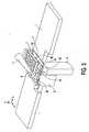
Fig. 3 , after the semiconductor products 21-26 have been wirebonded, thestationary clamp 4 releases thelead frame assembly 2 by moving in the Z direction to its second end position. - At this moment, or earlier in time, the
semiconductor products movable clamp 5 in its first end position. - As illustrated in
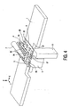
Figs. 4 and5 , theindex mechanism 6 then indexes thelead frame assembly 2 over twice the pitch of thesemiconductor products 3 in the X direction. Themovable clamp 5 and thewirebonding tool 7 follow the indexing movement of theindexing mechanism 6 by a suitable mechanical or electrical coupling therebetween, in particular between their respective (servo) drive motors. Meanwhile, thesemiconductor products - As illustrated in
Fig. 6 , next thelead frame assembly 2 is clamped by moving thestationary clamp 4 in the Z direction to its first end position. As a result,semiconductor products - Meanwhile, the
movable clamp 5 releases thelead frame assembly 2 by moving in the Z direction to its second end position. Theindex mechanism 6 then moves back to its former position relative to the wirebonding frame 1 of the wirebonding apparatus, taking themovable clamp 5 along, but without displacing thelead frame assembly 2. Themovable clamp 5 then clamps leads andsemiconductor product 35 and an adjacent semiconductor product not shown inFig. 6 by moving in the Z direction to its first end position, after which the clamped semiconductor products can be wirebonded. - Thus, the situation of
Fig. 1 is obtained again, and a new cycle of wirebonding can be completed. These cycles can be repeated for as long as semiconductor products on thelead frame assembly 2 remain to be wirebonded. - As a further example, consider the situation in which the lead frame assembly comprises only two rows of lead frames carrying semiconductor products e.g. a row comprising
semiconductor products semiconductor products semiconductor products semiconductor products - As another example, consider again the situation in which the lead frame assembly comprises only two rows of lead frames carrying semiconductor products e.g. a row comprising
semiconductor products semiconductor products semiconductor products semiconductor products - From
Figs. 1-6 it will be clear that a meandering wirebonding path may followed over and across thelead frame assembly 2 by thewirebonding tool 7 for a minimum bonding time to be realized. However, other paths may be followed as well. The indexing of thelead frame assembly 2 is performed during the wirebonding process, which thus does not need to be interrupted for the indexing. - More than one
bonding tool 7 may be employed. - According to the above, a wirebonding method and apparatus have been disclosed in which the lead frame assembly indexing time is virtually taken out of the critical time path of the wirebonding process by using a clamping mechanism comprising a stationary clamp and a movable clamp.
- It should be noted that the above-mentioned embodiments illustrate rather than limit the invention, and that those skilled in the art will be able to design many alternative embodiments without departing from the scope of the appended claims. In the claims, any reference signs placed between parentheses shall not be construed as limiting the claim. The word "comprising" does not exclude the presence of other elements or steps than those listed in a claim. The word "a" or "an" preceding an element does not exclude the presence of a plurality of such elements.
Claims (9)
- A method for wirebonding leads of a plurality of lead frames being part of a lead frame assembly (2) by a wirebonding tool (7) to semiconductor products (3) mounted on the respective lead frames, the lead frame assembly (2) being indexable in an index direction relative to a wirebonding frame, and comprising a first row and an adjacent second row of lead frames as seen in the index direction, the lead frames being spaced from each other at a lead frame pitch in the index direction, the method characterized in it comprises the steps of:(a) clamping the leads of n (n ≥1) adjacent lead frames of the first row by a first clamp (4), and wirebonding the leads of the n lead frames of the first row to the corresponding semiconductor products (3);(b) clamping the leads of n adjacent lead frames of the second row to a second base member, and wirebonding the leads of the n lead frames of the second row to the corresponding semiconductor products (3);(c) releasing the first clamp (4) after step a);(d) indexing the lead frame assembly (2) over n lead frame pitches relative to the wirebonding frame after step (a), the second clamp (5) and the wirebonding tool following the index movement;(e) releasing the second clamp (5) after step (b);(f) moving the second clamp (5) opposite to the indexing direction over n lead frame pitches; and(g) repeating steps (a)-(f).
- The method according to claim 1, characterized in that after step (f), the n lead frames of the first row lead one lead frame pitch relative to the n lead frames of the second row.
- The method according to claim 1 or 2, characterized by at least one further row of lead frames adjacent to the first row at the side facing away from the second row of lead frames, the first clamp (4) in step (a) further clamping n lead frames of the further row adjacent the n lead frames of the first row.
- The method according to any of claims 1-3, characterized by at least one further row of lead frames adjacent to the second row at the side facing away from the first row of lead frames, the second clamp (5) in step (b) further clamping n lead frames of the further row adjacent the n lead frames of the second row.
- The method according to any of claims 1-4, characterized in that n is even.
- The method according to any of claims 1-5, characterized in that the first clamp (4) is stationary relative to the wirebonding frame, as seen in the index direction.
- Wirebonding apparatus for wirebonding leads of a plurality of lead frames being part of a lead frame assembly (2) to semiconductor products (3) mounted on the respective lead frames, the apparatus comprising:- a wirebonding frame (1);- an indexing device (6) for indexing the lead frame assembly in an index direction relative to the wirebonding frame (1)characterized in;- at least a first clamp (4) for clamping the leads of n (n ≥ 1) adjacent lead frames of a first row of lead frames as seen in the index direction, the first clamp being stationary in the index direction relative to the wirebonding frame;- at least a second clamp (5) for clamping the leads of n adjacent lead frames of a second row of lead frames adjacent the first row, the second clamp being movable in the index direction relative to the wirebonding frame; and- a wirebonding tool (7) for wirebonding the leads of the n lead frames of the first and the second row to the corresponding semiconductor products (3), the wirebonding tool (7) and the second clamp (5) follow the index movement of the lead frame assembly (2) by a suitable mechanical or electrical coupling therebetween.
- Wirebonding apparatus according to claim 7, characterized in that the wirebonding tool is adapted to perform a wirebonding operation during the movement of the second clamp (5).
- Wirebonding apparatus according to claim 7 or 8, characterized in that the first clamp (4) and the second clamp (5) are situated generally opposite to each other, as seen transversely to the index direction.
Priority Applications (1)
| Application Number | Priority Date | Filing Date | Title |
|---|---|---|---|
| EP20030813211 EP1586111B1 (en) | 2002-12-18 | 2003-11-17 | Wirebonding method and apparatus |
Applications Claiming Priority (4)
| Application Number | Priority Date | Filing Date | Title |
|---|---|---|---|
| EP02080360 | 2002-12-18 | ||
| EP02080360 | 2002-12-18 | ||
| EP20030813211 EP1586111B1 (en) | 2002-12-18 | 2003-11-17 | Wirebonding method and apparatus |
| PCT/IB2003/005244 WO2004055870A1 (en) | 2002-12-18 | 2003-11-17 | Wirebonding method and apparatus |
Publications (2)
| Publication Number | Publication Date |
|---|---|
| EP1586111A1 EP1586111A1 (en) | 2005-10-19 |
| EP1586111B1 true EP1586111B1 (en) | 2009-04-15 |
Family
ID=32524045
Family Applications (1)
| Application Number | Title | Priority Date | Filing Date |
|---|---|---|---|
| EP20030813211 Expired - Lifetime EP1586111B1 (en) | 2002-12-18 | 2003-11-17 | Wirebonding method and apparatus |
Country Status (9)
| Country | Link |
|---|---|
| US (2) | US7578425B2 (en) |
| EP (1) | EP1586111B1 (en) |
| JP (1) | JP2006511066A (en) |
| KR (1) | KR20050084355A (en) |
| AT (1) | ATE429030T1 (en) |
| AU (1) | AU2003276600A1 (en) |
| DE (1) | DE60327258D1 (en) |
| TW (1) | TW200414386A (en) |
| WO (1) | WO2004055870A1 (en) |
Families Citing this family (6)
| Publication number | Priority date | Publication date | Assignee | Title |
|---|---|---|---|---|
| US7216794B2 (en) * | 2005-06-09 | 2007-05-15 | Texas Instruments Incorporated | Bond capillary design for ribbon wire bonding |
| EP1984945A2 (en) | 2006-02-10 | 2008-10-29 | Nxp B.V. | A semiconductor process system having an optical instrument comprising an apparatus for aligning an optical device with an object |
| JP2010182911A (en) * | 2009-02-06 | 2010-08-19 | Renesas Electronics Corp | Manufacturing method of semiconductor device and wire bonder |
| WO2011011298A2 (en) * | 2009-07-20 | 2011-01-27 | Kulicke And Soffa Industries, Inc. | Method of operating a clamping system of a wire bonding machine |
| WO2012092058A2 (en) * | 2010-12-29 | 2012-07-05 | Orthodyne Electroncis Corporation | Methods and systems for aligning tooling elements of ultrasonic bonding systems |
| MY183541A (en) * | 2016-03-01 | 2021-02-25 | Carsem M Sdn Bhd | Flexible window clamp |
Family Cites Families (3)
| Publication number | Priority date | Publication date | Assignee | Title |
|---|---|---|---|---|
| US5238174A (en) * | 1991-11-15 | 1993-08-24 | Kulicke And Soffa Investments, Inc. | Smart indexing head for universal lead frame work station |
| US6068174A (en) * | 1996-12-13 | 2000-05-30 | Micro)N Technology, Inc. | Device and method for clamping and wire-bonding the leads of a lead frame one set at a time |
| US6062459A (en) * | 1998-04-29 | 2000-05-16 | Advanced Micro Devices, Inc. | Wire bond clamp |
-
2003
- 2003-11-17 WO PCT/IB2003/005244 patent/WO2004055870A1/en not_active Ceased
- 2003-11-17 AU AU2003276600A patent/AU2003276600A1/en not_active Abandoned
- 2003-11-17 KR KR1020057011125A patent/KR20050084355A/en not_active Abandoned
- 2003-11-17 DE DE60327258T patent/DE60327258D1/en not_active Expired - Lifetime
- 2003-11-17 US US10/538,281 patent/US7578425B2/en not_active Expired - Fee Related
- 2003-11-17 AT AT03813211T patent/ATE429030T1/en not_active IP Right Cessation
- 2003-11-17 EP EP20030813211 patent/EP1586111B1/en not_active Expired - Lifetime
- 2003-11-17 JP JP2004559986A patent/JP2006511066A/en active Pending
- 2003-12-15 TW TW92135394A patent/TW200414386A/en unknown
-
2009
- 2009-07-20 US US12/506,065 patent/US8474680B2/en not_active Expired - Fee Related
Also Published As
| Publication number | Publication date |
|---|---|
| US20090277950A1 (en) | 2009-11-12 |
| EP1586111A1 (en) | 2005-10-19 |
| US20060016860A1 (en) | 2006-01-26 |
| AU2003276600A1 (en) | 2004-07-09 |
| TW200414386A (en) | 2004-08-01 |
| US7578425B2 (en) | 2009-08-25 |
| WO2004055870A1 (en) | 2004-07-01 |
| US8474680B2 (en) | 2013-07-02 |
| KR20050084355A (en) | 2005-08-26 |
| JP2006511066A (en) | 2006-03-30 |
| ATE429030T1 (en) | 2009-05-15 |
| DE60327258D1 (en) | 2009-05-28 |
Similar Documents
| Publication | Publication Date | Title |
|---|---|---|
| US8474680B2 (en) | Wirebonding method and apparatus | |
| US5735449A (en) | Method and apparatus for bonding semiconductor electronic devices | |
| US5813590A (en) | Extended travel wire bonding machine | |
| US6467672B2 (en) | Methods for clamping and wire-bonding the leads of a lead frame one set at a time | |
| JPH0620085B2 (en) | Welding equipment | |
| US8573468B1 (en) | Ultrasonic bonding systems and methods of using the same | |
| EP3790129A1 (en) | Ultrasonic processing device and ultrasonic processing method | |
| US4838472A (en) | Orthogonal axis device with linear motors for positioning and bonding wires onto electronic components | |
| CA1088281A (en) | Attaching leads to integrated-circuit chips | |
| US12087674B2 (en) | Spring bar leadframe, method and packaged electronic device with zero draft angle | |
| KR20190080776A (en) | Bonding and indexing apparatus | |
| JP2685029B2 (en) | Wire bonding equipment | |
| US20250140739A1 (en) | Laser enhanced wire bonding for semiconductor device packages | |
| KR100368626B1 (en) | Wire bonding method and apparatus | |
| JP2790085B2 (en) | Semiconductor device manufacturing method and manufacturing apparatus | |
| KR100273881B1 (en) | Wire bonding method | |
| JP2620355B2 (en) | Semiconductor device manufacturing method and manufacturing apparatus | |
| JP2000183096A (en) | Semiconductor device, wire bonding method for the semiconductor device, and wire bonder | |
| JP2526790B2 (en) | Semiconductor manufacturing equipment | |
| JPS5850762A (en) | Lead frame for semiconductor device | |
| JPH06350013A (en) | Lead frame, semiconductor device and manufacture of semiconductor device |
Legal Events
| Date | Code | Title | Description |
|---|---|---|---|
| PUAI | Public reference made under article 153(3) epc to a published international application that has entered the european phase |
Free format text: ORIGINAL CODE: 0009012 |
|
| 17P | Request for examination filed |
Effective date: 20050718 |
|
| AK | Designated contracting states |
Kind code of ref document: A1 Designated state(s): AT BE BG CH CY CZ DE DK EE ES FI FR GB GR HU IE IT LI LU MC NL PT RO SE SI SK TR |
|
| AX | Request for extension of the european patent |
Extension state: AL LT LV MK |
|
| DAX | Request for extension of the european patent (deleted) | ||
| RAP1 | Party data changed (applicant data changed or rights of an application transferred) |
Owner name: NXP B.V. |
|
| 17Q | First examination report despatched |
Effective date: 20070801 |
|
| GRAP | Despatch of communication of intention to grant a patent |
Free format text: ORIGINAL CODE: EPIDOSNIGR1 |
|
| GRAP | Despatch of communication of intention to grant a patent |
Free format text: ORIGINAL CODE: EPIDOSNIGR1 |
|
| GRAS | Grant fee paid |
Free format text: ORIGINAL CODE: EPIDOSNIGR3 |
|
| GRAA | (expected) grant |
Free format text: ORIGINAL CODE: 0009210 |
|
| AK | Designated contracting states |
Kind code of ref document: B1 Designated state(s): AT BE BG CH CY CZ DE DK EE ES FI FR GB GR HU IE IT LI LU MC NL PT RO SE SI SK TR |
|
| REG | Reference to a national code |
Ref country code: CH Ref legal event code: EP Ref country code: GB Ref legal event code: FG4D |
|
| REG | Reference to a national code |
Ref country code: IE Ref legal event code: FG4D |
|
| REF | Corresponds to: |
Ref document number: 60327258 Country of ref document: DE Date of ref document: 20090528 Kind code of ref document: P |
|
| NLV1 | Nl: lapsed or annulled due to failure to fulfill the requirements of art. 29p and 29m of the patents act | ||
| PG25 | Lapsed in a contracting state [announced via postgrant information from national office to epo] |
Ref country code: FI Free format text: LAPSE BECAUSE OF FAILURE TO SUBMIT A TRANSLATION OF THE DESCRIPTION OR TO PAY THE FEE WITHIN THE PRESCRIBED TIME-LIMIT Effective date: 20090415 Ref country code: AT Free format text: LAPSE BECAUSE OF FAILURE TO SUBMIT A TRANSLATION OF THE DESCRIPTION OR TO PAY THE FEE WITHIN THE PRESCRIBED TIME-LIMIT Effective date: 20090415 Ref country code: PT Free format text: LAPSE BECAUSE OF FAILURE TO SUBMIT A TRANSLATION OF THE DESCRIPTION OR TO PAY THE FEE WITHIN THE PRESCRIBED TIME-LIMIT Effective date: 20090915 Ref country code: ES Free format text: LAPSE BECAUSE OF FAILURE TO SUBMIT A TRANSLATION OF THE DESCRIPTION OR TO PAY THE FEE WITHIN THE PRESCRIBED TIME-LIMIT Effective date: 20090726 |
|
| PG25 | Lapsed in a contracting state [announced via postgrant information from national office to epo] |
Ref country code: SI Free format text: LAPSE BECAUSE OF FAILURE TO SUBMIT A TRANSLATION OF THE DESCRIPTION OR TO PAY THE FEE WITHIN THE PRESCRIBED TIME-LIMIT Effective date: 20090415 Ref country code: SE Free format text: LAPSE BECAUSE OF FAILURE TO SUBMIT A TRANSLATION OF THE DESCRIPTION OR TO PAY THE FEE WITHIN THE PRESCRIBED TIME-LIMIT Effective date: 20090715 Ref country code: NL Free format text: LAPSE BECAUSE OF FAILURE TO SUBMIT A TRANSLATION OF THE DESCRIPTION OR TO PAY THE FEE WITHIN THE PRESCRIBED TIME-LIMIT Effective date: 20090415 |
|
| PG25 | Lapsed in a contracting state [announced via postgrant information from national office to epo] |
Ref country code: EE Free format text: LAPSE BECAUSE OF FAILURE TO SUBMIT A TRANSLATION OF THE DESCRIPTION OR TO PAY THE FEE WITHIN THE PRESCRIBED TIME-LIMIT Effective date: 20090415 Ref country code: RO Free format text: LAPSE BECAUSE OF FAILURE TO SUBMIT A TRANSLATION OF THE DESCRIPTION OR TO PAY THE FEE WITHIN THE PRESCRIBED TIME-LIMIT Effective date: 20090415 Ref country code: CZ Free format text: LAPSE BECAUSE OF FAILURE TO SUBMIT A TRANSLATION OF THE DESCRIPTION OR TO PAY THE FEE WITHIN THE PRESCRIBED TIME-LIMIT Effective date: 20090415 Ref country code: DK Free format text: LAPSE BECAUSE OF FAILURE TO SUBMIT A TRANSLATION OF THE DESCRIPTION OR TO PAY THE FEE WITHIN THE PRESCRIBED TIME-LIMIT Effective date: 20090415 |
|
| PLBE | No opposition filed within time limit |
Free format text: ORIGINAL CODE: 0009261 |
|
| STAA | Information on the status of an ep patent application or granted ep patent |
Free format text: STATUS: NO OPPOSITION FILED WITHIN TIME LIMIT |
|
| PG25 | Lapsed in a contracting state [announced via postgrant information from national office to epo] |
Ref country code: BE Free format text: LAPSE BECAUSE OF FAILURE TO SUBMIT A TRANSLATION OF THE DESCRIPTION OR TO PAY THE FEE WITHIN THE PRESCRIBED TIME-LIMIT Effective date: 20090415 Ref country code: SK Free format text: LAPSE BECAUSE OF FAILURE TO SUBMIT A TRANSLATION OF THE DESCRIPTION OR TO PAY THE FEE WITHIN THE PRESCRIBED TIME-LIMIT Effective date: 20090415 |
|
| 26N | No opposition filed |
Effective date: 20100118 |
|
| PG25 | Lapsed in a contracting state [announced via postgrant information from national office to epo] |
Ref country code: BG Free format text: LAPSE BECAUSE OF FAILURE TO SUBMIT A TRANSLATION OF THE DESCRIPTION OR TO PAY THE FEE WITHIN THE PRESCRIBED TIME-LIMIT Effective date: 20090715 |
|
| PG25 | Lapsed in a contracting state [announced via postgrant information from national office to epo] |
Ref country code: MC Free format text: LAPSE BECAUSE OF NON-PAYMENT OF DUE FEES Effective date: 20091130 |
|
| REG | Reference to a national code |
Ref country code: CH Ref legal event code: PL |
|
| PG25 | Lapsed in a contracting state [announced via postgrant information from national office to epo] |
Ref country code: CH Free format text: LAPSE BECAUSE OF NON-PAYMENT OF DUE FEES Effective date: 20091130 Ref country code: LI Free format text: LAPSE BECAUSE OF NON-PAYMENT OF DUE FEES Effective date: 20091130 Ref country code: IE Free format text: LAPSE BECAUSE OF NON-PAYMENT OF DUE FEES Effective date: 20091117 Ref country code: GR Free format text: LAPSE BECAUSE OF FAILURE TO SUBMIT A TRANSLATION OF THE DESCRIPTION OR TO PAY THE FEE WITHIN THE PRESCRIBED TIME-LIMIT Effective date: 20090716 |
|
| PG25 | Lapsed in a contracting state [announced via postgrant information from national office to epo] |
Ref country code: IT Free format text: LAPSE BECAUSE OF FAILURE TO SUBMIT A TRANSLATION OF THE DESCRIPTION OR TO PAY THE FEE WITHIN THE PRESCRIBED TIME-LIMIT Effective date: 20090415 |
|
| PG25 | Lapsed in a contracting state [announced via postgrant information from national office to epo] |
Ref country code: LU Free format text: LAPSE BECAUSE OF NON-PAYMENT OF DUE FEES Effective date: 20091117 |
|
| PG25 | Lapsed in a contracting state [announced via postgrant information from national office to epo] |
Ref country code: HU Free format text: LAPSE BECAUSE OF FAILURE TO SUBMIT A TRANSLATION OF THE DESCRIPTION OR TO PAY THE FEE WITHIN THE PRESCRIBED TIME-LIMIT Effective date: 20091016 |
|
| PG25 | Lapsed in a contracting state [announced via postgrant information from national office to epo] |
Ref country code: TR Free format text: LAPSE BECAUSE OF FAILURE TO SUBMIT A TRANSLATION OF THE DESCRIPTION OR TO PAY THE FEE WITHIN THE PRESCRIBED TIME-LIMIT Effective date: 20090415 |
|
| PG25 | Lapsed in a contracting state [announced via postgrant information from national office to epo] |
Ref country code: CY Free format text: LAPSE BECAUSE OF FAILURE TO SUBMIT A TRANSLATION OF THE DESCRIPTION OR TO PAY THE FEE WITHIN THE PRESCRIBED TIME-LIMIT Effective date: 20090415 |
|
| REG | Reference to a national code |
Ref country code: GB Ref legal event code: 732E Free format text: REGISTERED BETWEEN 20110915 AND 20110921 |
|
| REG | Reference to a national code |
Ref country code: FR Ref legal event code: TP Owner name: INVENSAS CORPORATION, US Effective date: 20111014 |
|
| REG | Reference to a national code |
Ref country code: DE Ref legal event code: R082 Ref document number: 60327258 Country of ref document: DE Representative=s name: RGTH RICHTER GERBAULET THIELEMANN HOFMANN PATE, DE Effective date: 20120412 Ref country code: DE Ref legal event code: R081 Ref document number: 60327258 Country of ref document: DE Owner name: INVENSAS CORP., (N. D. GES. D. STAATES DELAWAR, US Free format text: FORMER OWNER: NXP B.V., EINDHOVEN, NL Effective date: 20120412 |
|
| REG | Reference to a national code |
Ref country code: FR Ref legal event code: CA Effective date: 20120724 |
|
| REG | Reference to a national code |
Ref country code: FR Ref legal event code: PLFP Year of fee payment: 13 |
|
| REG | Reference to a national code |
Ref country code: FR Ref legal event code: PLFP Year of fee payment: 14 |
|
| REG | Reference to a national code |
Ref country code: FR Ref legal event code: PLFP Year of fee payment: 15 |
|
| PGFP | Annual fee paid to national office [announced via postgrant information from national office to epo] |
Ref country code: DE Payment date: 20181128 Year of fee payment: 16 |
|
| PGFP | Annual fee paid to national office [announced via postgrant information from national office to epo] |
Ref country code: GB Payment date: 20181127 Year of fee payment: 16 Ref country code: FR Payment date: 20181127 Year of fee payment: 16 |
|
| REG | Reference to a national code |
Ref country code: DE Ref legal event code: R119 Ref document number: 60327258 Country of ref document: DE |
|
| GBPC | Gb: european patent ceased through non-payment of renewal fee |
Effective date: 20191117 |
|
| PG25 | Lapsed in a contracting state [announced via postgrant information from national office to epo] |
Ref country code: GB Free format text: LAPSE BECAUSE OF NON-PAYMENT OF DUE FEES Effective date: 20191117 Ref country code: FR Free format text: LAPSE BECAUSE OF NON-PAYMENT OF DUE FEES Effective date: 20191130 Ref country code: DE Free format text: LAPSE BECAUSE OF NON-PAYMENT OF DUE FEES Effective date: 20200603 |