EP1585372B1 - Electronic ballast with resonance excitation for voltage generation takeover - Google Patents
Electronic ballast with resonance excitation for voltage generation takeover Download PDFInfo
- Publication number
- EP1585372B1 EP1585372B1 EP05004714.1A EP05004714A EP1585372B1 EP 1585372 B1 EP1585372 B1 EP 1585372B1 EP 05004714 A EP05004714 A EP 05004714A EP 1585372 B1 EP1585372 B1 EP 1585372B1
- Authority
- EP
- European Patent Office
- Prior art keywords
- frequency
- lamp
- resonant circuit
- excitation
- switching transistors
- Prior art date
- Legal status (The legal status is an assumption and is not a legal conclusion. Google has not performed a legal analysis and makes no representation as to the accuracy of the status listed.)
- Not-in-force
Links
Images
Classifications
-
- H—ELECTRICITY
- H05—ELECTRIC TECHNIQUES NOT OTHERWISE PROVIDED FOR
- H05B—ELECTRIC HEATING; ELECTRIC LIGHT SOURCES NOT OTHERWISE PROVIDED FOR; CIRCUIT ARRANGEMENTS FOR ELECTRIC LIGHT SOURCES, IN GENERAL
- H05B41/00—Circuit arrangements or apparatus for igniting or operating discharge lamps
- H05B41/14—Circuit arrangements
- H05B41/26—Circuit arrangements in which the lamp is fed by power derived from dc by means of a converter, e.g. by high-voltage dc
- H05B41/28—Circuit arrangements in which the lamp is fed by power derived from dc by means of a converter, e.g. by high-voltage dc using static converters
- H05B41/288—Circuit arrangements in which the lamp is fed by power derived from dc by means of a converter, e.g. by high-voltage dc using static converters with semiconductor devices and specially adapted for lamps without preheating electrodes, e.g. for high-intensity discharge lamps, high-pressure mercury or sodium lamps or low-pressure sodium lamps
- H05B41/2881—Load circuits; Control thereof
- H05B41/2882—Load circuits; Control thereof the control resulting from an action on the static converter
- H05B41/2883—Load circuits; Control thereof the control resulting from an action on the static converter the controlled element being a DC/AC converter in the final stage, e.g. by harmonic mode starting
-
- H—ELECTRICITY
- H05—ELECTRIC TECHNIQUES NOT OTHERWISE PROVIDED FOR
- H05B—ELECTRIC HEATING; ELECTRIC LIGHT SOURCES NOT OTHERWISE PROVIDED FOR; CIRCUIT ARRANGEMENTS FOR ELECTRIC LIGHT SOURCES, IN GENERAL
- H05B41/00—Circuit arrangements or apparatus for igniting or operating discharge lamps
- H05B41/14—Circuit arrangements
- H05B41/36—Controlling
- H05B41/38—Controlling the intensity of light
- H05B41/382—Controlling the intensity of light during the transitional start-up phase
- H05B41/388—Controlling the intensity of light during the transitional start-up phase for a transition from glow to arc
-
- Y—GENERAL TAGGING OF NEW TECHNOLOGICAL DEVELOPMENTS; GENERAL TAGGING OF CROSS-SECTIONAL TECHNOLOGIES SPANNING OVER SEVERAL SECTIONS OF THE IPC; TECHNICAL SUBJECTS COVERED BY FORMER USPC CROSS-REFERENCE ART COLLECTIONS [XRACs] AND DIGESTS
- Y02—TECHNOLOGIES OR APPLICATIONS FOR MITIGATION OR ADAPTATION AGAINST CLIMATE CHANGE
- Y02B—CLIMATE CHANGE MITIGATION TECHNOLOGIES RELATED TO BUILDINGS, e.g. HOUSING, HOUSE APPLIANCES OR RELATED END-USER APPLICATIONS
- Y02B20/00—Energy efficient lighting technologies, e.g. halogen lamps or gas discharge lamps
Definitions
- This invention relates to electronic ballasts and methods of operating high pressure discharge lamps.
- WO 2004/064457 describes a half-bridge circuit with two half-bridge switches, which is suitable for operating a high-pressure discharge lamp.
- the circuit includes an LC resonant circuit, which is excited by a third switch.
- an ignition voltage at a considerable height must be provided, for example in a range of 1.5 kV to 5 kV (single amplitude).
- the ignited lamp needs for a certain transitional period a so-called. Takeover voltage, which is increased compared to the necessary voltage of the continuous operation power supply.
- the invention is based on the technical problem of providing an electronic ballast for operating a high-pressure discharge lamp and a corresponding operating method in which the transfer voltage can be generated and controlled in a favorable manner.
- the invention relates to an electronic ballast for operating a high-pressure discharge lamp with a converter comprising a half-bridge with two switching transistors for generating a supply power for continuous operation of the lamp by a switching operation of the switching transistors and with a filter capacitor for filtering rippling interference in the power supply for the lamp the filter capacitor is part of a resonant circuit.
- the ballast is designed to excite a resonance of the resonant circuit by high-frequency operation of the switching transistors of the converter so as to produce an over-voltage compared to the steady-state supply power for the lamp during an adjoining to an ignition acquisition phase.
- a control of the amplitude of the resonance excitation is carried out according to the invention also characterized in that - similar to the buck converter operation during lamp end operation - during a conductive switching phase of the switching transistors by repeated switching off ("chopping") with a respect to the resonant frequency significantly increased frequency quasi an average amplitude reduction is achieved. Additionally or alternatively, the time duration of the switch-on of the switching transistors can be limited in total and turn out to be significantly less than half a time proportion.
- the invention relates to a corresponding lighting device with such a ballast and a suitable high-pressure discharge lamp and finally to a corresponding operating method for operating a high-pressure discharge lamp.
- the basic idea of the invention is to generate the transfer voltage by means of a resonance excitation and to use the filter capacitor as the capacitive element of a resonant circuit, which is anyway is provided for filtering the Ripplestromanomanteile.
- the excitation of the resonant circuit should be done by the same converter, with which the continuous operation of the lamp is accomplished. So it should be exploited as possible already existing components of the circuit.
- the switching operation of the switching transistors which are also used for continuous operation, to be used for resonance excitation.
- the resonance excitation takes place with an excitation fundamental frequency of the switching operation of the switching transistors (S 1 , S 2 ).
- the turn-on of the respective conductive switching transistor is interrupted with a modulation frequency that is above the frequency for resonance excitation, which can be described by "chopping" or modulation.
- the invention thus offers the advantage of producing and controlling the required increased transfer voltages with little effort, without the so-called DC link voltage with which the converter i. d. R. is to be increased significantly.
- an inductor element of the resonance circuit used for other reasons anyway lamp inductor or Tiefsetzerdrossel is used.
- Such a choke is necessary on the one hand because of the in many cases partially negative differential impedance of high-pressure discharge lamps and / or on the other hand because of the below-described buck converter function.
- no further elements are provided in the resonant circuit as actually involved in the resonance elements, of course, the filter capacitor and the lamp inductor can be multi-part, as mentioned earlier for the filter capacitor.
- the half-bridge according to the invention can be operated in continuous operation of the lamp so that it on the one hand as a low-frequency inverter for the already described at the outset "symmetrization" of the lamp operation by Sign reversal works.
- the lamp operation can also be done with a reduced voltage compared to the intermediate circuit voltage, to which the half-bridge with the respective conductive switching transistor within a half-cycle of the inverter operation similar to a buck converter reduces the DC link voltage.
- This buck converter operation of the switching transistors of the half-bridge can be integrated into a lamp current control.
- the resonant excitation characteristic of the invention is preferably at a frequency below the resonant frequency of the resonant circuit.
- the use of resonance peaks in electronic ballasts for lamps approaches resonance frequencies coming from above. In the present case, this should be reversed.
- the lamp choke or another resonance choke should not be unnecessarily large for cost and space reasons. If, due to the recharging processes during the resonant excitation, saturation of the choke occurs, its inductance would change and the resonant circuit would automatically increase its resonant frequency. This would lead to an unstable state and to a considerable component load when approaching higher frequencies. In order to control such unstable conditions, relatively fast regulators and relatively fast voltage or current measurements are necessary. The invention circumvents this problem by approaching low frequencies.
- the fundamental frequency of resonance excitation is meant. Since the excitation is usually not done with pure sine functions but with more or less rectangular shaped functions, of course Fourier shares occur at frequencies above the resonant frequency. However, these have correspondingly lower amplitudes.
- a preferred value for the excitation frequency should preferably not be above 0.9 times the resonance frequency.
- the excitation frequency is not less than 0.4 times the resonant frequency, although in many cases no excessive resonance peak is necessary to produce a sufficient transfer voltage. This is because the square wave functions have a strong harmonic at three times the fundamental frequency, which approach the resonant frequency at fundamental frequencies below 0.4 times the resonant frequency. Convenient values are between 0.4 and 0.6 times the resonant frequency. However, within the scope of this invention, it is also quite possible to work with relatively low excitation frequencies which are significantly below the 0.4-fold resonance frequency.
- the filter capacitor should have a certain minimum capacity in favor of a good filter effect. Preference is given to values of more than 1 nF / watt lamp power, in particular of more than 1.2 or 1.3 nF / watt. Of course, with multiple capacitors this applies to the total effective capacity.
- the occurring voltage increases should preferably lead to amplitudes in the range of up to 800 V (single amplitude).
- to generate the ignition voltage by resonance peaking leads to significantly larger currents and to a much greater proximity to the resonant frequency. This results in adverse effects on the allowable capacitance of the filter capacitor, which serves as a resonant capacitor, and / or for the design of the throttle.
- the ignition voltage itself is preferably generated by its own ignition circuit. This may in particular be a per se known ignition circuit with a firing capacitor whose discharge, possibly after high transformation, leads to the ignition.
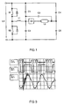
- FIG. 1 shows a known per se half-bridge topology with two switching transistors S 1 and S 2 . These are connected in series between two supply branches, between which an intermediate circuit voltage U 1 is present.
- the intermediate circuit voltage U 1 can be generated by rectifying a mains voltage with appropriate filtering and possibly power factor correction.
- the coupling capacitors C 4 and C 5 ensure that the right terminal of the lamp Lp has a potential in the middle between the potentials of the supply branches. Thus, the circuit is thus able to generate half the DC link voltage across the lamp Lp.
- Parallel to the lamp Lp is a filter capacitor C 3rd
- a tap between the lamp inductor L 1 and the ignition circuit G 1 is connected via two filter capacitors C 1 and C 2 respectively to the supply branches.
- a burning voltage of the order of magnitude of 80 V-150 V is necessary, which is actually smaller than the commonly available halved intermediate circuit voltages. Therefore, during a switching phase, in which, for example, the half-bridge transistor S 1 is conducting, it is interrupted in a clocked manner, in order to produce, together with the inductor L 1 during this switching phase To generate buck converter operation. As a result, a desired lamp burn voltage can be set by the step-down operation.
- a high-pressure discharge lamp requires a certain period of time for the transition from a glow discharge following the actual ignition to the arc discharge, in which a takeover voltage which is significantly higher than the burning voltage must be available in the range of typically 260 V-330 V. This value is regularly above the halved DC link voltage.
- the half-bridge combined with the buck converter can not easily generate this voltage.
- a resonance of a lamp resonant circuit is excited during the acquisition phase, which consists of the capacitors C 1 - C 3 and the inductor L 1 .
- This causes a voltage increase, with which the desired transfer voltage can be generated.
- this resonant excitation is used only for the transfer voltage and not for the ignition voltage, so that the filter capacitors a desired size of typically 50 nF in a ballast for a 35 W lamp or 100 nF in a ballast for a 70 W lamp and corresponding Capacities at other lamp power can have. This is in fact the effective total capacity of the capacitors C 1 to C 3 .
- Said resonant excitation for generating the transfer voltage is carried out according to the invention at lower frequencies than the resonant frequency of the lamp resonant circuit, in this embodiment, approximately at the halved resonant frequency, namely at 0.55 times the resonant frequency.
- a fast controller and a fast voltage or current measurement on the lamp resonant circuit can thus be avoided.
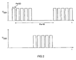
- FIG. 2 schematically shows the timing of the switching operation of the two transistors S 1 and S 2 FIG. 1 ,
- the upper part stands for the upper transistor S 1 (UGS1)
- the lower part stands for the lower transistor S 2 (UGS2).
- two periods occur here, namely a longer period between the pulse packets (PerHB) and, secondly, a shorter period within the pulse packets (PerSD).
- PerHB pulse packets
- PerSD pulse packets
- this corresponds to the already described combination of down-converter operation and half-bridge function, wherein the short period stands for the step-down operation and the longer one for the half-bridge function.
- FIG. 3 shows a real diagram of the ballast circuit FIG. 1 ,
- the uppermost curve at channel 1 shows the gate voltage of the lower half-bridge transistor S 2 , the middle curve at channel 2 the potential of the half-bridge midpoint and the lower curve at channel 3 the voltage across the lamp.
- the clear deflection of the lamp voltage approximately at the end of the first box from the left shows the ignition of the lamp with the aid of the ignition circuit G 1 .
- the thus excited high-frequency resonance is for the invention of no further concern and has to do with leakage inductances of the ignition circuit G 1 in connection with certain capacities.
- FIG. 2 illustrated "chopped" rectangular switching operation of the half-bridge transistor is already present before the ignition. Although it causes no ignition and therefore no acquisition, it does not hurt either. There does not even have to be synchronization to the ignition process. Rather, the described "chopped" half-bridge operation ensures a resonant (0.55-fold resonant frequency) excitation with a corresponding voltage overshoot across the lamp.
- FIG. 3 shows, voltage amplitudes across the lamp of almost ⁇ 400 V.
- This excitation takes place with the AC voltage shown at channel 2 at the bridge center.
- Typical resonance frequencies are approximately at 20 kHz - 40 kHz.
- the total effective capacitance of the filter capacitors is 100 nF and the inductance of the inductor L 1 is 500 ⁇ H.
- the basic excitation frequency is 12.5 kHz, the resonance frequency about 22.5 kHz.
- the amount of the takeover voltage can therefore be adjusted by the choice of the excitation frequency, on the one hand, and by the "chopper operation" on the other hand, and of course by the temporal extension of the conducting phases of the switching transistors.
- FIG. 3 shows that the "chopper frequency" is about 8 times the basic excitation frequency.
- a duty cycle within the modulation frequency ie a ratio between the switch-on phase and the associated switch-off phase by the "chopping", of about 85% is reached (the Dutycicle is only related to the modulation and not to the basic cycle).
Description
Diese Erfindung bezieht sich auf elektronische Vorschaltgeräte und Betriebsverfahren für Hochdruckentladungslampen.This invention relates to electronic ballasts and methods of operating high pressure discharge lamps.
In der Schrift
In der Schrift
In der Schrift
In der Schrift
In der Schrift
In der Schrift
Es ist an sich bekannt, Hochdruckentladungslampen mit elektronischen Vorschaltgeräten zu betreiben, die Wandler mit einem oder einer Mehrzahl Schalttransistoren aufweisen. Häufig sind Vollbrückenwandler. Während des Dauerbetriebs der Lampe erzeugen diese Wandler vereinfacht ausgedrückt in ihrer Polarität niederfrequent alternierende Gleichspannungs-Versorgungsleistungen für die Lampe. Dabei werden bei einem echten und damit asymmetrischen Gleichstrombetrieb auftretende störende Phänomene in der Lampe vermieden und gleichzeitig ebenfalls störende höhere Frequenzen von der Lampe weitgehend ferngehalten.It is known per se to operate high-pressure discharge lamps with electronic ballasts having transducers with one or a plurality of switching transistors. Often full bridge converters. During continuous operation of the lamp, these converters, in simplified terms, produce in their polarity low-frequency alternating DC power supplies for the lamp. In this case, occurring in a real and thus asymmetric DC operation disturbing phenomena in the lamp are avoided and at the same time also disturbing higher frequencies largely kept away from the lamp.
Es ist insbesondere notwendig, mit Filterkondensatoren verbleibende sog. Ripplestromanteile in der Versorgungsleistung für die Lampe auszufiltern bzw. zu begrenzen. Im Folgenden ist dabei von einem Filterkondensator die Rede, womit allerdings auch Varianten mit einer Mehrzahl Filterkondensatoren gemeint sind.In particular, it is necessary to filter out or limit so-called ripple current components remaining in the supply power for the lamp with filter capacitors. In the following, we are talking about a filter capacitor, which, however, also means variants with a plurality of filter capacitors.
Wenn Hochdruckentladungslampen gezündet werden, muss eine Zündspannung in erheblicher Höhe zur Verfügung gestellt werden, beispielsweise in einem Bereich von 1,5 kV bis 5 kV (einfache Amplitude). Die gezündete Lampe benötigt für eine gewisse Übergangszeit eine sog. Übernahmespannung, die gegenüber der notwendigen Spannung der Dauerbetriebs-Versorgungsleistung erhöht ist.When high-pressure discharge lamps are ignited, an ignition voltage at a considerable height must be provided, for example in a range of 1.5 kV to 5 kV (single amplitude). The ignited lamp needs for a certain transitional period a so-called. Takeover voltage, which is increased compared to the necessary voltage of the continuous operation power supply.
Der Erfindung liegt das technische Problem zugrunde, ein elektronisches Vorschaltgerät zum Betreiben einer Hochdruckentladungslampe und ein entsprechendes Betriebsverfahren anzugeben, bei denen in einer günstigen Weise die Übernahmespannung erzeugt und kontrolliert werden kann.The invention is based on the technical problem of providing an electronic ballast for operating a high-pressure discharge lamp and a corresponding operating method in which the transfer voltage can be generated and controlled in a favorable manner.
Die Erfindung bezieht sich auf ein elektronisches Vorschaltgerät zum Betreiben einer Hochdruckentladungslampe mit einem Wandler beinhaltend eine Halbbrücke mit zwei Schalttransistoren zum Erzeugen einer Versorgungsleistung zum Dauerbetrieb der Lampe durch einen Schaltbetrieb der Schalttransistoren und mit einem Filterkondensator zum Filtern von Ripplestörungen in der Versorgungsleistung für die Lampe, wobei der Filterkondensator Teil einer Resonanzschaltung ist. Das Vorschaltgerät ist dazu ausgelegt, durch einen hochfrequenten Betrieb der Schalttransistoren des Wandlers eine Resonanz der Resonanzschaltung anzuregen, um damit eine gegenüber der Dauerbetriebs-Versorgungsleistung spannungsüberhöhte Leistung für die Lampe während einer an eine Zündung anschließende Übernahmephase zu erzeugen.The invention relates to an electronic ballast for operating a high-pressure discharge lamp with a converter comprising a half-bridge with two switching transistors for generating a supply power for continuous operation of the lamp by a switching operation of the switching transistors and with a filter capacitor for filtering rippling interference in the power supply for the lamp the filter capacitor is part of a resonant circuit. The ballast is designed to excite a resonance of the resonant circuit by high-frequency operation of the switching transistors of the converter so as to produce an over-voltage compared to the steady-state supply power for the lamp during an adjoining to an ignition acquisition phase.
Eine Steuerung der Amplitude der Resonanzanregung erfolgt erfindungsgemäß auch dadurch, dass - ähnlich dem Tiefsetzerbetrieb während des Lampendauerbetriebs - während einer leitenden Schaltphase der Schalttransistoren durch ein wiederholtes Ausschalten ("Zerhacken") mit einer gegenüber der Resonanzfrequenz deutlich erhöhten Frequenz quasi eine mittlere Amplitudenabsenkung erreicht wird. Zusätzlich oder alternativ kann auch die zeitliche Dauer der Einschaltphase der Schalttransistoren insgesamt begrenzt werden und deutlich geringer als ein hälftiger Zeitanteil ausfallen.A control of the amplitude of the resonance excitation is carried out according to the invention also characterized in that - similar to the buck converter operation during lamp end operation - during a conductive switching phase of the switching transistors by repeated switching off ("chopping") with a respect to the resonant frequency significantly increased frequency quasi an average amplitude reduction is achieved. Additionally or alternatively, the time duration of the switch-on of the switching transistors can be limited in total and turn out to be significantly less than half a time proportion.
Weiterhin bezieht sich die Erfindung auf ein entsprechendes Beleuchtungsgerät mit einem solchen Vorschaltgerät und einer passenden Hochdruckentladungslampe und schließlich auf ein entsprechendes Betriebsverfahren zum Betreiben einer Hochdruckentladungslampe.Furthermore, the invention relates to a corresponding lighting device with such a ballast and a suitable high-pressure discharge lamp and finally to a corresponding operating method for operating a high-pressure discharge lamp.
Bevorzugte Ausgestaltungen sind in den abhängigen Ansprüchen angegeben.Preferred embodiments are specified in the dependent claims.
Die Grundidee der Erfindung besteht darin, die Übernahmespannung durch eine Resonanzanregung zu erzeugen und dabei als kapazitives Element einer Resonanzschaltung den Filterkondensator zu verwenden, der ohnehin zum Ausfiltern der Ripplestromanteile vorgesehen ist. Die Anregung der Resonanzschaltung soll durch denselben Wandler erfolgen, mit dem der Dauerbetrieb der Lampe bewerkstelligt wird. Es sollen also möglichst ohnehin vorhandene Bestandteile der Schaltung ausgenutzt werden. Insbesondere soll der Schaltbetrieb der Schalttransistoren, die auch für den Dauerbetrieb verwendet werden, zur Resonanzanregung eingesetzt werden. Die Resonanzanregung erfolgt mit einer Anregungsgrundfrequenz des Schaltbetriebs der Schalttransistoren (S1, S2). Die Einschaltphase des jeweils leitenden Schalttransistors wird mit einer Modulationsfrequenz, die über der Frequenz zur Resonanzanregung liegt, unterbrochen, was durch "Zerhacken" oder Modulation beschrieben werden kann.The basic idea of the invention is to generate the transfer voltage by means of a resonance excitation and to use the filter capacitor as the capacitive element of a resonant circuit, which is anyway is provided for filtering the Ripplestromanomanteile. The excitation of the resonant circuit should be done by the same converter, with which the continuous operation of the lamp is accomplished. So it should be exploited as possible already existing components of the circuit. In particular, the switching operation of the switching transistors, which are also used for continuous operation, to be used for resonance excitation. The resonance excitation takes place with an excitation fundamental frequency of the switching operation of the switching transistors (S 1 , S 2 ). The turn-on of the respective conductive switching transistor is interrupted with a modulation frequency that is above the frequency for resonance excitation, which can be described by "chopping" or modulation.
Insgesamt bietet die Erfindung damit den Vorteil, mit einem geringen Aufwand die erforderlichen erhöhten Übernahmespannungen zu erzeugen und zu kontrollieren, ohne deswegen die sog. Zwischenkreisspannung, mit der der Wandler i. d. R. versorgt wird, deutlich erhöhen zu müssen.Overall, the invention thus offers the advantage of producing and controlling the required increased transfer voltages with little effort, without the so-called DC link voltage with which the converter i. d. R. is to be increased significantly.
Vorzugsweise wird als induktives Element der Resonanzschaltung eine aus anderen Gründen ohnehin vorhandene Lampendrossel oder Tiefsetzerdrossel verwendet. Eine solche Drossel ist zum einen wegen der in vielen Fällen teilweise negativen differentiellen Impedanz von Hochdruckentladungslampen und/oder zum anderen wegen der im Folgenden noch erläuterten Tiefsetzerfunktion notwendig. Vorzugsweise sind dabei in der Resonanzschaltung als eigentlich an der Resonanz beteiligte Elemente keine weiteren Elemente vorgesehen, wobei natürlich der Filterkondensator und die Lampendrossel mehrteilig sein können, wie für den Filterkondensator bereits früher erwähnt.Preferably, an inductor element of the resonance circuit used for other reasons anyway lamp inductor or Tiefsetzerdrossel is used. Such a choke is necessary on the one hand because of the in many cases partially negative differential impedance of high-pressure discharge lamps and / or on the other hand because of the below-described buck converter function. Preferably, no further elements are provided in the resonant circuit as actually involved in the resonance elements, of course, the filter capacitor and the lamp inductor can be multi-part, as mentioned earlier for the filter capacitor.
Die erfindungsgemäße Halbbrücke kann im Dauerbetrieb der Lampe so betrieben werden, dass sie einerseits als niederfrequenter Inverter für die bereits eingangs geschilderte "Symmetrisierung" des Lampenbetriebs durch Vorzeichenumkehr arbeitet. Andererseits kann der Lampenbetrieb dabei außerdem mit einer gegenüber der Zwischenkreisspannung herabgesetzten Spannung erfolgen, wozu die Halbbrücke mit dem jeweils leitenden Schalttransistor innerhalb einer Halbperiode des Inverterbetriebs ähnlich einem Tiefsetzer die Zwischenkreisspannung herabsetzt. Dieser Tiefsetzerbetrieb der Schalttransistoren der Halbbrücke kann in eine Lampenstromregelung eingebunden sein.The half-bridge according to the invention can be operated in continuous operation of the lamp so that it on the one hand as a low-frequency inverter for the already described at the outset "symmetrization" of the lamp operation by Sign reversal works. On the other hand, the lamp operation can also be done with a reduced voltage compared to the intermediate circuit voltage, to which the half-bridge with the respective conductive switching transistor within a half-cycle of the inverter operation similar to a buck converter reduces the DC link voltage. This buck converter operation of the switching transistors of the half-bridge can be integrated into a lamp current control.
Die für die Erfindung charakteristische Resonanzanregung erfolgt vorzugsweise mit einer Frequenz unterhalb der Resonanzfrequenz der Resonanzschaltung. Konventioneller Weise nähert man sich bei der Ausnutzung von Resonanzüberhöhungen in elektronischen Vorschaltgeräten für Lampen Resonanzfrequenzen von oben her kommend an. Im vorliegenden Fall soll dies umgekehrt erfolgen. Dies hat aus folgenden Gründen Vorteile: Eine gute Filterwirkung des Filterkondensators bedingt eine gewisse Mindestkapazität des Filterkondensators. Andererseits soll die Lampendrossel oder eine andere Resonanzdrossel aus Kosten- und Platzgründen nicht unnötig groß sein. Wenn es nun durch die Umladevorgänge bei der Resonanzanregung zu einer Sättigung der Drossel kommt, so würde sich deren Induktivität verändern und die Resonanzschaltung selbsttätig ihre Resonanzfrequenz erhöhen. Dies würde bei einer Annäherung von höheren Frequenzen her zu einem instabilen Zustand und zu einer erheblichen Bauteilbelastung führen. Um solche instabilen Verhältnisse kontrollieren zu können, sind relativ schnelle Regler und relativ schnelle Spannungs- oder Strommessungen notwendig. Die Erfindung umgeht dieses Problem durch Annäherung von tiefen Frequenzen her.The resonant excitation characteristic of the invention is preferably at a frequency below the resonant frequency of the resonant circuit. Conventionally, the use of resonance peaks in electronic ballasts for lamps approaches resonance frequencies coming from above. In the present case, this should be reversed. This has advantages for the following reasons: A good filter effect of the filter capacitor requires a certain minimum capacitance of the filter capacitor. On the other hand, the lamp choke or another resonance choke should not be unnecessarily large for cost and space reasons. If, due to the recharging processes during the resonant excitation, saturation of the choke occurs, its inductance would change and the resonant circuit would automatically increase its resonant frequency. This would lead to an unstable state and to a considerable component load when approaching higher frequencies. In order to control such unstable conditions, relatively fast regulators and relatively fast voltage or current measurements are necessary. The invention circumvents this problem by approaching low frequencies.
Dabei ist hier die Grundfrequenz der Resonanzanregung gemeint. Da die Anregung im Regelfall nicht mit reinen Sinusfunktionen sondern mit mehr oder weniger rechteckig geformten Funktionen erfolgen wird, können natürlich Fourieranteile mit Frequenzen über der Resonanzfrequenz auftreten. Diese haben jedoch entsprechend geringere Amplituden.Here, the fundamental frequency of resonance excitation is meant. Since the excitation is usually not done with pure sine functions but with more or less rectangular shaped functions, of course Fourier shares occur at frequencies above the resonant frequency. However, these have correspondingly lower amplitudes.
Ein bevorzugter Wert für die Anregungsfrequenz sollte möglichst nicht über dem 0,9-fachen der Resonanzfrequenz liegen. Andererseits kann es vorteilhaft sein, wenn die Anregungsfrequenz, obwohl in vielen Fällen keine allzu starke Resonanzüberhöhung notwendig ist, um eine ausreichende Übernahmespannung zu erzeugen, nicht unter dem 0,4-fachen der Resonanzfrequenz liegt. Dies liegt daran, dass die Rechteckfunktionen eine starke Harmonische bei der dreifachen Grundfrequenz aufweisen, die bei Grundfrequenzen unterhalb der 0,4-fachen Resonanzfrequenz nah an die Resonanzfrequenz heranrücken. Günstig sind Werte zwischen dem 0,4- und 0,6-fachen der Resonanzfrequenz. Allerdings ist es im Rahmen dieser Erfindung auch durchaus möglich, mit relativ niedrigen Anregungsfrequenzen zu arbeiten, die deutlich unterhalb der 0,4-fachen Resonanzfrequenz liegen. Dabei ist dann die Spannungserhöhung im Sinne einer Sprungantwort zu verstehen, erfolgt also gewissermaßen hauptsächlich durch die Oberschwingungen des Anregungssprungs. (Mit Anregungssprung ist hier allerdings nicht eine einmalige Anregung sondern lediglich die Tatsache gemeint, dass die Frequenz deutlich kleiner als die Resonanzfrequenz ist.)A preferred value for the excitation frequency should preferably not be above 0.9 times the resonance frequency. On the other hand, it may be advantageous if the excitation frequency is not less than 0.4 times the resonant frequency, although in many cases no excessive resonance peak is necessary to produce a sufficient transfer voltage. This is because the square wave functions have a strong harmonic at three times the fundamental frequency, which approach the resonant frequency at fundamental frequencies below 0.4 times the resonant frequency. Convenient values are between 0.4 and 0.6 times the resonant frequency. However, within the scope of this invention, it is also quite possible to work with relatively low excitation frequencies which are significantly below the 0.4-fold resonance frequency. In this case, then, the voltage increase in the sense of a step response is to be understood, so to speak, takes place mainly by the harmonics of the excitation jump. (With excitation jump here is not meant a one-time excitation but only the fact that the frequency is much smaller than the resonance frequency.)
Es wurde bereits erwähnt, dass der Filterkondensator zu Gunsten einer guten Filterwirkung eine gewisse Mindestkapazität aufweisen soll. Bevorzugt sind Werte von mehr als 1 nF/Watt Lampenleistung, insbesondere von mehr als 1,2 oder 1,3 nF/Watt. Bei mehreren Kondensatoren gilt dies natürlich für die effektive Gesamtkapazität.It has already been mentioned that the filter capacitor should have a certain minimum capacity in favor of a good filter effect. Preference is given to values of more than 1 nF / watt lamp power, in particular of more than 1.2 or 1.3 nF / watt. Of course, with multiple capacitors this applies to the total effective capacity.
Die auftretenden Spannungsüberhöhungen sollten vorzugsweise zu Amplituden im Bereich von bis zu 800 V (einfache Amplitude) führen. Es ist nämlich insbesondere bevorzugt, mit der erfindungsgemäßen Resonanzüberhöhung nur die Übernahmespannung und nicht die Zündspannung zu erzeugen. Auch die Zündspannung durch Resonanzüberhöhung zu erzeugen, führt zu erheblich größeren Strömen und zu einer erheblich größeren Nähe zur Resonanzfrequenz. Damit ergeben sich nachteilige Auswirkungen für die zulässige Kapazität des Filterkondensators, der als Resonanzkondensator dient, und/oder für die Bemessung der Drossel. Da aber angestrebt wird, mit einem ausreichend großen Filterkondensator einerseits und mit einer nicht zu großen Lampendrossel bzw. anderen Resonanzdrossel andererseits zu arbeiten, wird die Zündspannung selbst vorzugsweise durch eine eigene Zündschaltung erzeugt. Dabei kann es sich insbesondere um eine an sich bekannte Zündschaltung mit einem Zündkondensator handeln, dessen Entladung, ggf. nach Hochtransformation, zur Zündung führt.The occurring voltage increases should preferably lead to amplitudes in the range of up to 800 V (single amplitude). In fact, it is particularly preferred with the resonance peaking according to the invention to generate only the transfer voltage and not the ignition voltage. Also, to generate the ignition voltage by resonance peaking, leads to significantly larger currents and to a much greater proximity to the resonant frequency. This results in adverse effects on the allowable capacitance of the filter capacitor, which serves as a resonant capacitor, and / or for the design of the throttle. However, since the aim is to work with a sufficiently large filter capacitor on the one hand and with a not too large lamp choke or other resonance choke on the other hand, the ignition voltage itself is preferably generated by its own ignition circuit. This may in particular be a per se known ignition circuit with a firing capacitor whose discharge, possibly after high transformation, leads to the ignition.
Im Folgenden wird die Erfindung anhand eines Ausführungsbeispiels näher erläutert. Insbesondere bezieht sich die vorstehende wie die nachfolgende Beschreibung immer sowohl auf die Vorrichtungs- als auch auf die Verfahrenskategorie der Erfindung.
- Figur 1
- zeigt ein schematisches Schaltdiagramm eines erfindungsgemäßen Vorschaltgeräts.
Figur 2- zeigt schematisierte Zeitverlaufsdiagramme zur Illustration der Taktung von Transistoren des Vorschaltgeräts aus
Figur 1 . - Figur 3
- zeigt Messdiagramme zum Betrieb des Vorschaltgeräts aus
Figur 1 bei einer Taktung gemäßFigur 2
- FIG. 1
- shows a schematic circuit diagram of a ballast according to the invention.
- FIG. 2
- shows schematic timing diagrams for illustrating the timing of transistors of the ballast
FIG. 1 , - FIG. 3
- shows measurement diagrams for the operation of the ballast
FIG. 1 at a timing according toFIG. 2 ,
Durch einen alternierenden Schaltbetrieb der Halbbrückentransistoren S1 und S2 wird ein Mittenabgriff dazwischen hin und her geschaltet zwischen den Potentialen der Versorgungsäste. Dementsprechend liegt an dem linken Anschluss einer in
Im tatsächlichen Betrieb einer Hochdruckentladungslampe ist eine Brennspannung von größenordnungsmäßig 80 V - 150 V notwendig, die tatsächlich kleiner ist als die üblicherweise zur Verfügung stehenden halbierten Zwischenkreisspannungen. Daher wird hier während einer Schaltphase, in der beispielsweise der Halbbrückentransistor S1 leitend ist, dieser getaktet unterbrochen, um gemeinsam mit der Drossel L1 während dieser Schaltphase einen Tiefsetzerbetrieb zu erzeugen. Dadurch kann durch den Tiefsetzerbetrieb eine gewünschte Lampenbrennspannung eingestellt werden.In actual operation of a high-pressure discharge lamp, a burning voltage of the order of magnitude of 80 V-150 V is necessary, which is actually smaller than the commonly available halved intermediate circuit voltages. Therefore, during a switching phase, in which, for example, the half-bridge transistor S 1 is conducting, it is interrupted in a clocked manner, in order to produce, together with the inductor L 1 during this switching phase To generate buck converter operation. As a result, a desired lamp burn voltage can be set by the step-down operation.
Andererseits benötigt eine Hochdruckentladungslampe für den Übergang von einer sich an die eigentliche Zündung anschließenden Glimmentladung in die Bogenentladung eine gewisse Zeitdauer, in der eine gegenüber der Brennspannung deutlich überhöhte Übernahmespannung im Bereich von typischerweise 260 V - 330 V zur Verfügung stehen muss. Dieser Wert liegt regelmäßig über der halbierten Zwischenkreisspannung. Die mit dem Tiefsetzer kombinierte Halbbrücke kann diese Spannung nicht ohne weiteres erzeugen.On the other hand, a high-pressure discharge lamp requires a certain period of time for the transition from a glow discharge following the actual ignition to the arc discharge, in which a takeover voltage which is significantly higher than the burning voltage must be available in the range of typically 260 V-330 V. This value is regularly above the halved DC link voltage. The half-bridge combined with the buck converter can not easily generate this voltage.
Erfindungsgemäß wird während der Übernahmephase eine Resonanz eines Lampenresonanzkreises angeregt, der aus den Kondensatoren C1 - C3 und der Drossel L1 besteht. Dadurch wird eine Spannungsüberhöhung bewirkt, mit der die gewünschte Übernahmespannung erzeugt werden kann. Erfindungsgemäß wird diese Resonanzanregung jedoch nur für die Übernahmespannung und nicht für die Zündspannung verwendet, so dass die Filterkondensatoren eine gewünschte Größe von typischerweise 50 nF bei einem Vorschaltgerät für eine 35 W-Lampe oder 100 nF bei einem Vorschaltgerät für eine 70 W-Lampe und entsprechenden Kapazitäten bei anderen Lampenleistungen haben können. Dabei handelt es sich faktisch um die effektive Gesamtkapazität der Kondensatoren C1 bis C3. Würde mit dieser effektiven Filterkapazität eine Resonanzzündung erfolgen, so würden in Folge der notwendigen Zündspannungen von größenordnungsmäßig 1,5 kV - 5 kV zusammen mit der genannten Kapazität erhebliche Ströme entstehen. Die Drossel L1 müsste dementsprechend sehr groß dimensioniert werden, um die damit korrelierende Energie aufnehmen zu können. (Diese Energie ist proportional zur Filterkapazität und zum Quadrat der Spannung.) Eine solche Drosseldimensionierung wird gemäß der Erfindung als hinsichtlich der Baugröße und der Kosten ungünstig angesehen.According to the invention a resonance of a lamp resonant circuit is excited during the acquisition phase, which consists of the capacitors C 1 - C 3 and the inductor L 1 . This causes a voltage increase, with which the desired transfer voltage can be generated. According to the invention, however, this resonant excitation is used only for the transfer voltage and not for the ignition voltage, so that the filter capacitors a desired size of typically 50 nF in a ballast for a 35 W lamp or 100 nF in a ballast for a 70 W lamp and corresponding Capacities at other lamp power can have. This is in fact the effective total capacity of the capacitors C 1 to C 3 . If a resonant ignition were to take place with this effective filter capacity, considerable currents would arise as a result of the necessary ignition voltages of the order of magnitude of 1.5 kV-5 kV together with the stated capacity. Accordingly, the throttle L 1 would have to be dimensioned very large in order to be able to absorb the energy correlating therewith. (This energy is proportional to the filter capacitance and the square of the voltage.) Such a throttle sizing is considered unfavorable according to the invention in terms of size and cost.
Eine Erhöhung der Zwischenkreisspannung käme zwar als Lösung in Betracht, ist jedoch wegen der Dimensionierung der Bauteile der Halbbrücke und einer eventuellen Leistungsfaktorkorrekturschaltung und auch beim Wirkungsgrad mit Nachteilen verbunden.Although an increase in the intermediate circuit voltage would be considered as a solution, however, it is associated with disadvantages because of the dimensioning of the components of the half-bridge and a possible power factor correction circuit and also in terms of efficiency.
Die genannte Resonanzanregung zur Erzeugung der Übernahmespannung erfolgt erfindungsgemäß bei geringeren Frequenzen als die Resonanzfrequenz des Lampenresonanzkreises, bei diesem Ausführungsbeispiel etwa bei der halbierten Resonanzfrequenz, und zwar bei dem 0,55-fachen der Resonanzfrequenz. Damit entstehen nur moderate Spannungsüberhöhungen, die jedoch für die Übernahmephase völlig ausreichen. Insbesondere ist durch die Frequenzlage unterhalb der Resonanzfrequenz sichergestellt, dass es bei eventuellen unbeabsichtigten Sättigungserscheinungen oder anderen Schwankungen nicht zu grundsätzlichen Instabilitäten kommt. Insbesondere können damit ein schneller Regler und eine schnelle Spannungs- oder Strommessung an dem Lampenresonanzkreis vermieden werden.Said resonant excitation for generating the transfer voltage is carried out according to the invention at lower frequencies than the resonant frequency of the lamp resonant circuit, in this embodiment, approximately at the halved resonant frequency, namely at 0.55 times the resonant frequency. This results in only moderate voltage overshoots, which are, however, completely sufficient for the acquisition phase. In particular, it is ensured by the frequency position below the resonant frequency that there is no fundamental instability in case of any unintended saturation phenomena or other fluctuations. In particular, a fast controller and a fast voltage or current measurement on the lamp resonant circuit can thus be avoided.
Hier geht es allerdings um den Betrieb während der Übernahmephase. Die längere Periode steht hierbei für die resonanznahe Anregung bei etwa der 0,55-fachen Resonanzfrequenz. Innerhalb der entsprechenden, durch das hochliegende Niveau der Gatespannung des entsprechenden Transistors dargestellten leitenden Phase erfolgt eine "Zerhackung", also eine Modulation mit der kürzeren Periodendauer. Diese liegt deutlich über der Resonanzfrequenz, könnte aber in bestimmten Fällen auch kleiner als die Resonanzfrequenz sein. Es sollte lediglich vermieden werden, zu stark in die Nähe der Resonanzfrequenz zu geraten. Mit der "Zerhackung" kann gewissermaßen die effektive wirksame Amplitude der rechteckförmigen Anregung mit der 0,55-fachen Resonanzfrequenz vermindert werden. Durch eine "Zerhackung" mit deutlich höherer Frequenz ist für den Resonanzkreis gewissermaßen nur der Mittelwert relevant. Eine Ergänzung oder Alternative würde übrigens darin bestehen, die Einschaltphasen gegenüber dem hälftigen Zeitanteil zu verkürzen, also gewissermaßen die "Zerhackerpulse" synchron an den Anfang oder das Ende einer leitenden Phase zu setzen.However, this is about the operation during the acquisition phase. The longer period stands for resonance-near excitation at about the 0.55-fold resonance frequency. Within the corresponding, represented by the high level of the gate voltage of the corresponding transistor conductive phase is a "chopping", ie a modulation with the shorter period. This is well above the resonance frequency, but in certain cases could be smaller than the resonance frequency. It should only be avoided to get too close to the resonance frequency. With the "chopping" can be effectively reduced the effective effective amplitude of the rectangular excitation with the 0.55-fold resonant frequency. By "chopping" with a much higher frequency, only the mean value is to some extent relevant for the resonance circuit. Incidentally, a supplement or alternative would be to shorten the switch-on phases compared to the half-time component, ie to set the "chopper pulses" synchronously at the beginning or the end of a conducting phase.
Der deutliche Ausschlag der Lampenspannung etwa am Ende des ersten Kästchens von links zeigt die Zündung der Lampe mit Hilfe der Zündschaltung G1. Die dadurch angeregte hochfrequente Resonanz ist für die Erfindung nicht von weiterem Belangen und hat mit Streuinduktivitäten der Zündschaltung G1 in Verbindung mit bestimmten Kapazitäten zu tun. Man erkennt jedoch, dass der anhand
Typische Resonanzfrequenzen liegen etwa bei 20 kHz - 40 kHz. Im vorliegenden Fall beträgt die effektive Gesamtkapazität der Filterkondensatoren 100 nF und die Induktivität der Drossel L1 500 µH. Die Anregungsgrundfrequenz beträgt 12,5 kHz, die Resonanzfrequenz etwa 22,5 kHz.Typical resonance frequencies are approximately at 20 kHz - 40 kHz. In the present case, the total effective capacitance of the filter capacitors is 100 nF and the inductance of the inductor L 1 is 500 μH. The basic excitation frequency is 12.5 kHz, the resonance frequency about 22.5 kHz.
In der Lampenspannung auf Kanal 3 lässt sich erkennen, dass mit dem Übergang von der leitenden Schaltphase eines Schalttransistors zur leitenden Schaltphase des anderen näherungsweise eine Sinusperiode der Lampenspannung beginnt. Dabei entsprechen die beiden Schultern zwischen den Extremwerten der Lampenspannung dem Start und dem Ende solcher Sinusperioden, also näherungsweise den Extrema der einzelnen Sinusperiode. Es handelt sich um Sprungantworten auf die Resonanzanregung in Folge der gegenüber der Resonanzfrequenz deutlich niedrigeren Anregungsfrequenz. Dabei schwingt die Lampenspannung mit doppelter Anregungsamplitude durch und würde dann eine Sinusschwingung um die Anregungsamplitude herum durchführen, von der jedoch nur ein erstes Stück zu sehen ist. Dies liegt gerade an dem näherungsweise der Zahl 2 entsprechenden Verhältnis zwischen Anregungsfrequenz und Resonanzfrequenz.In the lamp voltage on channel 3, it can be seen that with the transition from the conducting switching phase of one switching transistor to the conducting switching phase of the other, approximately one sine period of the lamp voltage begins. The two shoulders between the extreme values of the lamp voltage correspond to the start and the end of such sine periods, ie approximately the extremes of the individual sine period. These are step responses to the resonance excitation as a result of the significantly lower excitation frequency than the resonance frequency. The lamp voltage oscillates with twice the excitation amplitude and would then perform a sinusoidal oscillation around the excitation amplitude, of which, however, only a first piece can be seen. This is precisely due to the ratio of the excitation frequency to the resonance frequency that corresponds approximately to the
Die Höhe der Übernahmespannung lässt sich also zum einen durch die Wahl der Anregungsfrequenz, zum anderen durch den "Zerhackerbetrieb" und zum dritten natürlich durch die zeitliche Ausdehnung der leitenden Phasen der Schalttransistoren einstellen.The amount of the takeover voltage can therefore be adjusted by the choice of the excitation frequency, on the one hand, and by the "chopper operation" on the other hand, and of course by the temporal extension of the conducting phases of the switching transistors.
Claims (11)
- Electronic ballast for operating a high-pressure discharge lamp (Lp) having- a converter containing a half-bridge having two switching transistors (S1, S2) for the purpose of generating an operating voltage for continuous operation of the lamp (Lp) by means of a switching operation of the switching transistors (S1, S2),- a resonant circuit (L1, C1-3),- a starting circuit (G1) having a starting capacitor for the purpose of starting the high-pressure discharge lamp by a discharge and possibly step-up transformation of the charging of the starting capacitor,wherein- the electronic ballast is designed to excite a resonance in the resonant circuit (L1, C1-3) by means of radiofrequency operation of the switching transistors (S1, S2) of the converter, in order thus to generate a voltage amplitude for the lamp (Lp), which is greater than the operating voltage, during a transfer phase following starting,- wherein the excitation of the resonance of the resonant circuit (L1, C1-3) takes place at a fundamental excitation frequency of the switching operation of the switching transistors (S1, S2),characterized in that- the fundamental excitation frequency of the switching operation of the switching transistors (S1, S2) is lower than a resonant frequency of the resonant circuit, and- the electronic ballast is designed to reduce the average voltage amplitude during the transfer phase by repeated disconnection in the switch-on phases of the switching transistors (S1, S2) at a frequency which is markedly higher than the fundamental excitation frequency, and- the resonant circuit has a filter capacitor (C1-3) for the purpose of filtering ripple interference in the operating voltage.
- Ballast according to Claim 1, in which the resonant circuit (L1, C1-3) contains a lamp inductor (L1) as the inductive element.
- Ballast according to Claim 1 or 2, in which the converter is designed to operate, during continuous operation of the lamp (Lp), as a low-frequency inverter and, within the inverter switching phases, as a step-down converter for the purpose of regulating the lamp current.
- Ballast according to one of the preceding claims, in which the resonance excitation takes place at a fundamental frequency of at most 0.9 times the resonant frequency of the resonant circuit (L1, C1-3).
- Ballast according to Claim 4, in which the resonance excitation takes place at a fundamental frequency between 0.4 times and 0.9 times, inclusive, the resonant frequency of the resonant circuit (L1, C1-3).
- Ballast according to Claim 1, in which the frequency of the repeated disconnection in the switch-on phases of the switching transistors (S1, S2) is markedly above the resonant frequency of the resonant circuit (L1, C1-3).
- Ballast according to one of the preceding claims, in which the capacitance of the filter capacitor (C1-3) is at least 1 nF/watt of lamp power.
- Ballast according to one of the preceding claims, in which the voltage amplitudes during resonance excitation are at most 800 V (peak-to-peak).
- Illumination device having a ballast according to one of Claims 1 - 8 and a high-pressure discharge lamp (Lp).
- Method for operating a high-pressure discharge lamp (Lp) having the following steps:- starting the high-pressure discharge lamp with a starting circuit (G1) having a starting capacitor by a discharge and possibly step-up transformation of the charging of the starting capacitor,- supplying an operating voltage to the lamp during continuous operation by means of a switching operation of two switching transistors (S1, S2) of a half-bridge converter,- during a transfer phase following starting, generating a voltage amplitude which is greater than the operating voltage by resonance excitation in a resonant circuit (L1, C1-3), wherein the resonance excitation takes place by means of radiofrequency operation of the switching transistors (S1, S2) of the half-bridge converter,characterized in that- the resonance excitation takes place by means of a fundamental excitation frequency of the switching operation of the switching transistors (S1, S2), whose frequency is lower than the resonant frequency of the resonant circuit,- the average voltage amplitude is reduced during the transfer phase by repeated disconnection in the switch-on phases of the switching transistors (S1, S2) at a frequency which is markedly higher than the fundamental excitation frequency,
and- ripple interference in the operating voltage of the lamp is filtered by a filter capacitor (C1-3) contained in the resonant circuit. - Method for operating a lamp (Lp) according to Claim 10 having a ballast according to one of Claims 2 - 8.
Applications Claiming Priority (2)
| Application Number | Priority Date | Filing Date | Title |
|---|---|---|---|
| DE102004017479A DE102004017479A1 (en) | 2004-04-08 | 2004-04-08 | ECG with resonance stimulus for transfer voltage generation |
| DE102004017479 | 2004-04-08 |
Publications (2)
| Publication Number | Publication Date |
|---|---|
| EP1585372A1 EP1585372A1 (en) | 2005-10-12 |
| EP1585372B1 true EP1585372B1 (en) | 2013-07-10 |
Family
ID=34895538
Family Applications (1)
| Application Number | Title | Priority Date | Filing Date |
|---|---|---|---|
| EP05004714.1A Not-in-force EP1585372B1 (en) | 2004-04-08 | 2005-03-03 | Electronic ballast with resonance excitation for voltage generation takeover |
Country Status (5)
| Country | Link |
|---|---|
| US (1) | US7145293B2 (en) |
| EP (1) | EP1585372B1 (en) |
| CN (1) | CN1681368A (en) |
| CA (1) | CA2503635A1 (en) |
| DE (1) | DE102004017479A1 (en) |
Families Citing this family (7)
| Publication number | Priority date | Publication date | Assignee | Title |
|---|---|---|---|---|
| US7432663B2 (en) * | 2006-09-25 | 2008-10-07 | Osram Sylvania Inc. | Circuit for igniting a high intensity discharge lamp |
| US7432664B2 (en) * | 2006-09-29 | 2008-10-07 | Osram Sylvania Inc. | Circuit for powering a high intensity discharge lamp |
| US8193728B2 (en) * | 2007-01-10 | 2012-06-05 | Osram Ag | Circuit arrangement and method for operating a high-pressure discharge lamp |
| WO2008128577A1 (en) * | 2007-04-24 | 2008-10-30 | Osram Gesellschaft mit beschränkter Haftung | Circuit arrangement for igniting and operating a discharge lamp |
| US8450939B2 (en) | 2007-05-07 | 2013-05-28 | Osram Ag | Method for igniting and starting high-pressure discharge lamps |
| DE102011089553A1 (en) * | 2011-12-22 | 2013-06-27 | Robert Bosch Gmbh | Electronic ballast for a gas discharge lamp |
| ITGE20120058A1 (en) * | 2012-06-20 | 2013-12-21 | Umpi R & D S R L | FEEDING SYSTEM FOR A PUBLIC LIGHTING SYSTEM WITH INTEGRATED AUXILIARY SERVICES |
Citations (3)
| Publication number | Priority date | Publication date | Assignee | Title |
|---|---|---|---|---|
| US5696798A (en) * | 1993-09-30 | 1997-12-09 | Rockwell Semiconductor Systems, Inc. | Multiple antenna home base for digital cordless telephones |
| DE19644115A1 (en) * | 1996-10-23 | 1998-04-30 | Patent Treuhand Ges Fuer Elektrische Gluehlampen Mbh | Circuit arrangement for operating a high-pressure discharge lamp and lighting system with a high-pressure discharge lamp and an operating device for the high-pressure discharge lamp |
| US20020047609A1 (en) * | 1997-12-12 | 2002-04-25 | Matsushita Electric Works R&D Laboratory | Ballast for discharge lamp |
Family Cites Families (12)
| Publication number | Priority date | Publication date | Assignee | Title |
|---|---|---|---|---|
| ATE147925T1 (en) * | 1992-08-20 | 1997-02-15 | Philips Electronics Nv | SWITCHGEAR FOR A LAMP |
| US5426350A (en) * | 1993-11-18 | 1995-06-20 | Electric Power Research Institute, Inc. | High frequency transformerless electronics ballast using double inductor-capacitor resonant power conversion for gas discharge lamps |
| DE19508468B4 (en) * | 1994-11-25 | 2006-05-24 | Matsushita Electric Works, Ltd., Kadoma | Power supply means |
| US5623187A (en) * | 1994-12-28 | 1997-04-22 | Philips Electronics North America Corporation | Controller for a gas discharge lamp with variable inverter frequency and with lamp power and bus voltage control |
| US5932976A (en) * | 1997-01-14 | 1999-08-03 | Matsushita Electric Works R&D Laboratory, Inc. | Discharge lamp driving |
| DK1042942T3 (en) * | 1997-07-24 | 2002-12-02 | Noontek Ltd | Electronic ballast for a gas discharge lamp |
| US6459215B1 (en) * | 2000-08-11 | 2002-10-01 | General Electric Company | Integral lamp |
| US6459214B1 (en) * | 2001-04-10 | 2002-10-01 | General Electric Company | High frequency/high power factor inverter circuit with combination cathode heating |
| DE10210629A1 (en) * | 2002-03-11 | 2003-09-25 | Knobel Lichttech | Ignition circuit for a high pressure discharge lamp |
| DE10235217A1 (en) * | 2002-08-01 | 2004-02-19 | Patent-Treuhand-Gesellschaft für elektrische Glühlampen mbH | Circuit device for operating lamp, especially low pressure discharge lamp has current limiter that can drive control electrode of at least one transistor switching unit in inverter to limit current |
| WO2004064457A1 (en) * | 2003-01-14 | 2004-07-29 | Koninklijke Philips Electronics N.V. | Circuit arrangment |
| US7075251B2 (en) * | 2003-12-05 | 2006-07-11 | General Electric Company | Universal platform for phase dimming discharge lighting ballast and lamp |
-
2004
- 2004-04-08 DE DE102004017479A patent/DE102004017479A1/en not_active Withdrawn
-
2005
- 2005-03-03 EP EP05004714.1A patent/EP1585372B1/en not_active Not-in-force
- 2005-04-06 CA CA002503635A patent/CA2503635A1/en not_active Abandoned
- 2005-04-08 US US11/101,390 patent/US7145293B2/en active Active
- 2005-04-08 CN CNA2005100648852A patent/CN1681368A/en active Pending
Patent Citations (3)
| Publication number | Priority date | Publication date | Assignee | Title |
|---|---|---|---|---|
| US5696798A (en) * | 1993-09-30 | 1997-12-09 | Rockwell Semiconductor Systems, Inc. | Multiple antenna home base for digital cordless telephones |
| DE19644115A1 (en) * | 1996-10-23 | 1998-04-30 | Patent Treuhand Ges Fuer Elektrische Gluehlampen Mbh | Circuit arrangement for operating a high-pressure discharge lamp and lighting system with a high-pressure discharge lamp and an operating device for the high-pressure discharge lamp |
| US20020047609A1 (en) * | 1997-12-12 | 2002-04-25 | Matsushita Electric Works R&D Laboratory | Ballast for discharge lamp |
Also Published As
| Publication number | Publication date |
|---|---|
| CA2503635A1 (en) | 2005-10-08 |
| EP1585372A1 (en) | 2005-10-12 |
| DE102004017479A1 (en) | 2005-10-27 |
| CN1681368A (en) | 2005-10-12 |
| US20050225260A1 (en) | 2005-10-13 |
| US7145293B2 (en) | 2006-12-05 |
Similar Documents
| Publication | Publication Date | Title |
|---|---|---|
| DE60024215T2 (en) | MODULAR HIGH FREQUENCY BALLAST | |
| EP0244644B1 (en) | Circuit arrangement for the high-frequency operation of low-pressure discharge lamps | |
| DE4420182B4 (en) | Power supply apparatus | |
| EP0669789B1 (en) | Circuit for operating at least one low-pressure discharge lamp | |
| EP1585372B1 (en) | Electronic ballast with resonance excitation for voltage generation takeover | |
| EP0356818B1 (en) | Circuitry for driving a load | |
| DE10025610A1 (en) | Control equipment for discharge lamp in start phase provides a d.c. component to lamp voltage to power transfer to arc discharge condition | |
| DE102005007346A1 (en) | Circuit arrangement and method for operating gas discharge lamps | |
| DE20221985U1 (en) | Electronic ballast for gas discharge lamp | |
| EP1465330B1 (en) | Method and circuit for varying the power consumption of capacitive loads | |
| DE60224094T2 (en) | ELECTRONIC CIRCUIT AND METHOD FOR OPERATING A HIGH-PRESSURE LAMP | |
| DE19606874A1 (en) | Power supply fed by DC source e.g. for high-pressure discharge lamp | |
| EP2399429A1 (en) | Electronic operating device for a gas discharge lamp | |
| DE3711814C2 (en) | Electronic ballast for operating fluorescent lamps | |
| WO2008128576A2 (en) | Circuit arrangement for igniting and operating a discharge lamp | |
| DE102008052701A1 (en) | Ignition device and lighting device | |
| EP1696713B1 (en) | Electronic ballast with current measuring means for high-pressure discharge lamps | |
| EP2417837B1 (en) | Circuit arrangement and method for operating a high-pressure discharge lamp | |
| EP2168229A1 (en) | Circuit arrangement comprising a voltage transformer and associated method | |
| EP1583403B1 (en) | Ballast for at least one lamp | |
| DE10206175A1 (en) | Discharge lamp lighting circuit | |
| EP0697803A2 (en) | Circuit for operating discharge lamps | |
| WO2005107339A1 (en) | Device for generation of voltage pulse sequences in particular for operation of capacitive discharge lamps | |
| DE112005000771T5 (en) | Discharge lamp lighting apparatus | |
| DE102005056229A1 (en) | Fluorescent lamp control circuit for aircraft industry, has feed lines between inductor and capacitance, where parasitic capacitance of switching unit and voltage of converter are added to provide starting voltage |
Legal Events
| Date | Code | Title | Description |
|---|---|---|---|
| PUAI | Public reference made under article 153(3) epc to a published international application that has entered the european phase |
Free format text: ORIGINAL CODE: 0009012 |
|
| AK | Designated contracting states |
Kind code of ref document: A1 Designated state(s): AT BE BG CH CY CZ DE DK EE ES FI FR GB GR HU IE IS IT LI LT LU MC NL PL PT RO SE SI SK TR |
|
| AX | Request for extension of the european patent |
Extension state: AL BA HR LV MK YU |
|
| 17P | Request for examination filed |
Effective date: 20051107 |
|
| AKX | Designation fees paid |
Designated state(s): AT BE BG CH CY CZ DE DK EE ES FI FR GB GR HU IE IS IT LI LT LU MC NL PL PT RO SE SI SK TR |
|
| 17Q | First examination report despatched |
Effective date: 20051208 |
|
| GRAP | Despatch of communication of intention to grant a patent |
Free format text: ORIGINAL CODE: EPIDOSNIGR1 |
|
| RAP1 | Party data changed (applicant data changed or rights of an application transferred) |
Owner name: OSRAM GMBH |
|
| RIC1 | Information provided on ipc code assigned before grant |
Ipc: H05B 41/288 20060101AFI20130305BHEP Ipc: H05B 41/38 20060101ALI20130305BHEP |
|
| RAP1 | Party data changed (applicant data changed or rights of an application transferred) |
Owner name: OSRAM GMBH |
|
| GRAS | Grant fee paid |
Free format text: ORIGINAL CODE: EPIDOSNIGR3 |
|
| GRAA | (expected) grant |
Free format text: ORIGINAL CODE: 0009210 |
|
| AK | Designated contracting states |
Kind code of ref document: B1 Designated state(s): AT BE BG CH CY CZ DE DK EE ES FI FR GB GR HU IE IS IT LI LT LU MC NL PL PT RO SE SI SK TR |
|
| REG | Reference to a national code |
Ref country code: GB Ref legal event code: FG4D Free format text: NOT ENGLISH |
|
| REG | Reference to a national code |
Ref country code: CH Ref legal event code: EP Ref country code: AT Ref legal event code: REF Ref document number: 621571 Country of ref document: AT Kind code of ref document: T Effective date: 20130715 |
|
| REG | Reference to a national code |
Ref country code: IE Ref legal event code: FG4D Free format text: LANGUAGE OF EP DOCUMENT: GERMAN |
|
| REG | Reference to a national code |
Ref country code: DE Ref legal event code: R096 Ref document number: 502005013824 Country of ref document: DE Effective date: 20130905 |
|
| PG25 | Lapsed in a contracting state [announced via postgrant information from national office to epo] |
Ref country code: SI Free format text: LAPSE BECAUSE OF FAILURE TO SUBMIT A TRANSLATION OF THE DESCRIPTION OR TO PAY THE FEE WITHIN THE PRESCRIBED TIME-LIMIT Effective date: 20130710 |
|
| REG | Reference to a national code |
Ref country code: NL Ref legal event code: VDEP Effective date: 20130710 |
|
| REG | Reference to a national code |
Ref country code: LT Ref legal event code: MG4D |
|
| PG25 | Lapsed in a contracting state [announced via postgrant information from national office to epo] |
Ref country code: SE Free format text: LAPSE BECAUSE OF FAILURE TO SUBMIT A TRANSLATION OF THE DESCRIPTION OR TO PAY THE FEE WITHIN THE PRESCRIBED TIME-LIMIT Effective date: 20130710 Ref country code: IS Free format text: LAPSE BECAUSE OF FAILURE TO SUBMIT A TRANSLATION OF THE DESCRIPTION OR TO PAY THE FEE WITHIN THE PRESCRIBED TIME-LIMIT Effective date: 20131110 Ref country code: LT Free format text: LAPSE BECAUSE OF FAILURE TO SUBMIT A TRANSLATION OF THE DESCRIPTION OR TO PAY THE FEE WITHIN THE PRESCRIBED TIME-LIMIT Effective date: 20130710 Ref country code: CY Free format text: LAPSE BECAUSE OF FAILURE TO SUBMIT A TRANSLATION OF THE DESCRIPTION OR TO PAY THE FEE WITHIN THE PRESCRIBED TIME-LIMIT Effective date: 20130619 Ref country code: PT Free format text: LAPSE BECAUSE OF FAILURE TO SUBMIT A TRANSLATION OF THE DESCRIPTION OR TO PAY THE FEE WITHIN THE PRESCRIBED TIME-LIMIT Effective date: 20131111 |
|
| PG25 | Lapsed in a contracting state [announced via postgrant information from national office to epo] |
Ref country code: PL Free format text: LAPSE BECAUSE OF FAILURE TO SUBMIT A TRANSLATION OF THE DESCRIPTION OR TO PAY THE FEE WITHIN THE PRESCRIBED TIME-LIMIT Effective date: 20130710 Ref country code: FI Free format text: LAPSE BECAUSE OF FAILURE TO SUBMIT A TRANSLATION OF THE DESCRIPTION OR TO PAY THE FEE WITHIN THE PRESCRIBED TIME-LIMIT Effective date: 20130710 Ref country code: NL Free format text: LAPSE BECAUSE OF FAILURE TO SUBMIT A TRANSLATION OF THE DESCRIPTION OR TO PAY THE FEE WITHIN THE PRESCRIBED TIME-LIMIT Effective date: 20130710 Ref country code: ES Free format text: LAPSE BECAUSE OF FAILURE TO SUBMIT A TRANSLATION OF THE DESCRIPTION OR TO PAY THE FEE WITHIN THE PRESCRIBED TIME-LIMIT Effective date: 20131021 Ref country code: GR Free format text: LAPSE BECAUSE OF FAILURE TO SUBMIT A TRANSLATION OF THE DESCRIPTION OR TO PAY THE FEE WITHIN THE PRESCRIBED TIME-LIMIT Effective date: 20131011 |
|
| PG25 | Lapsed in a contracting state [announced via postgrant information from national office to epo] |
Ref country code: CY Free format text: LAPSE BECAUSE OF FAILURE TO SUBMIT A TRANSLATION OF THE DESCRIPTION OR TO PAY THE FEE WITHIN THE PRESCRIBED TIME-LIMIT Effective date: 20130710 |
|
| PG25 | Lapsed in a contracting state [announced via postgrant information from national office to epo] |
Ref country code: EE Free format text: LAPSE BECAUSE OF FAILURE TO SUBMIT A TRANSLATION OF THE DESCRIPTION OR TO PAY THE FEE WITHIN THE PRESCRIBED TIME-LIMIT Effective date: 20130710 Ref country code: CZ Free format text: LAPSE BECAUSE OF FAILURE TO SUBMIT A TRANSLATION OF THE DESCRIPTION OR TO PAY THE FEE WITHIN THE PRESCRIBED TIME-LIMIT Effective date: 20130710 Ref country code: SK Free format text: LAPSE BECAUSE OF FAILURE TO SUBMIT A TRANSLATION OF THE DESCRIPTION OR TO PAY THE FEE WITHIN THE PRESCRIBED TIME-LIMIT Effective date: 20130710 Ref country code: RO Free format text: LAPSE BECAUSE OF FAILURE TO SUBMIT A TRANSLATION OF THE DESCRIPTION OR TO PAY THE FEE WITHIN THE PRESCRIBED TIME-LIMIT Effective date: 20130710 Ref country code: DK Free format text: LAPSE BECAUSE OF FAILURE TO SUBMIT A TRANSLATION OF THE DESCRIPTION OR TO PAY THE FEE WITHIN THE PRESCRIBED TIME-LIMIT Effective date: 20130710 |
|
| PLBE | No opposition filed within time limit |
Free format text: ORIGINAL CODE: 0009261 |
|
| STAA | Information on the status of an ep patent application or granted ep patent |
Free format text: STATUS: NO OPPOSITION FILED WITHIN TIME LIMIT |
|
| PG25 | Lapsed in a contracting state [announced via postgrant information from national office to epo] |
Ref country code: IT Free format text: LAPSE BECAUSE OF FAILURE TO SUBMIT A TRANSLATION OF THE DESCRIPTION OR TO PAY THE FEE WITHIN THE PRESCRIBED TIME-LIMIT Effective date: 20130710 |
|
| 26N | No opposition filed |
Effective date: 20140411 |
|
| REG | Reference to a national code |
Ref country code: DE Ref legal event code: R097 Ref document number: 502005013824 Country of ref document: DE Effective date: 20140411 |
|
| PG25 | Lapsed in a contracting state [announced via postgrant information from national office to epo] |
Ref country code: LU Free format text: LAPSE BECAUSE OF FAILURE TO SUBMIT A TRANSLATION OF THE DESCRIPTION OR TO PAY THE FEE WITHIN THE PRESCRIBED TIME-LIMIT Effective date: 20140303 |
|
| REG | Reference to a national code |
Ref country code: CH Ref legal event code: PL |
|
| REG | Reference to a national code |
Ref country code: IE Ref legal event code: MM4A |
|
| PG25 | Lapsed in a contracting state [announced via postgrant information from national office to epo] |
Ref country code: LI Free format text: LAPSE BECAUSE OF NON-PAYMENT OF DUE FEES Effective date: 20140331 Ref country code: CH Free format text: LAPSE BECAUSE OF NON-PAYMENT OF DUE FEES Effective date: 20140331 Ref country code: IE Free format text: LAPSE BECAUSE OF NON-PAYMENT OF DUE FEES Effective date: 20140303 |
|
| REG | Reference to a national code |
Ref country code: AT Ref legal event code: MM01 Ref document number: 621571 Country of ref document: AT Kind code of ref document: T Effective date: 20140303 |
|
| PG25 | Lapsed in a contracting state [announced via postgrant information from national office to epo] |
Ref country code: AT Free format text: LAPSE BECAUSE OF NON-PAYMENT OF DUE FEES Effective date: 20140303 |
|
| REG | Reference to a national code |
Ref country code: FR Ref legal event code: PLFP Year of fee payment: 12 |
|
| PG25 | Lapsed in a contracting state [announced via postgrant information from national office to epo] |
Ref country code: MC Free format text: LAPSE BECAUSE OF FAILURE TO SUBMIT A TRANSLATION OF THE DESCRIPTION OR TO PAY THE FEE WITHIN THE PRESCRIBED TIME-LIMIT Effective date: 20130710 Ref country code: BG Free format text: LAPSE BECAUSE OF FAILURE TO SUBMIT A TRANSLATION OF THE DESCRIPTION OR TO PAY THE FEE WITHIN THE PRESCRIBED TIME-LIMIT Effective date: 20130710 |
|
| PG25 | Lapsed in a contracting state [announced via postgrant information from national office to epo] |
Ref country code: BE Free format text: LAPSE BECAUSE OF FAILURE TO SUBMIT A TRANSLATION OF THE DESCRIPTION OR TO PAY THE FEE WITHIN THE PRESCRIBED TIME-LIMIT Effective date: 20140331 Ref country code: HU Free format text: LAPSE BECAUSE OF FAILURE TO SUBMIT A TRANSLATION OF THE DESCRIPTION OR TO PAY THE FEE WITHIN THE PRESCRIBED TIME-LIMIT; INVALID AB INITIO Effective date: 20050303 Ref country code: TR Free format text: LAPSE BECAUSE OF FAILURE TO SUBMIT A TRANSLATION OF THE DESCRIPTION OR TO PAY THE FEE WITHIN THE PRESCRIBED TIME-LIMIT Effective date: 20130710 |
|
| REG | Reference to a national code |
Ref country code: FR Ref legal event code: PLFP Year of fee payment: 13 |
|
| REG | Reference to a national code |
Ref country code: FR Ref legal event code: PLFP Year of fee payment: 14 |
|
| PGFP | Annual fee paid to national office [announced via postgrant information from national office to epo] |
Ref country code: DE Payment date: 20190321 Year of fee payment: 15 Ref country code: FR Payment date: 20190322 Year of fee payment: 15 Ref country code: GB Payment date: 20190320 Year of fee payment: 15 |
|
| REG | Reference to a national code |
Ref country code: DE Ref legal event code: R119 Ref document number: 502005013824 Country of ref document: DE |
|
| PG25 | Lapsed in a contracting state [announced via postgrant information from national office to epo] |
Ref country code: DE Free format text: LAPSE BECAUSE OF NON-PAYMENT OF DUE FEES Effective date: 20201001 Ref country code: FR Free format text: LAPSE BECAUSE OF NON-PAYMENT OF DUE FEES Effective date: 20200331 |
|
| GBPC | Gb: european patent ceased through non-payment of renewal fee |
Effective date: 20200303 |
|
| PG25 | Lapsed in a contracting state [announced via postgrant information from national office to epo] |
Ref country code: GB Free format text: LAPSE BECAUSE OF NON-PAYMENT OF DUE FEES Effective date: 20200303 |