EP1585193B1 - Breitbandantenne - Google Patents
Breitbandantenne Download PDFInfo
- Publication number
- EP1585193B1 EP1585193B1 EP05012924A EP05012924A EP1585193B1 EP 1585193 B1 EP1585193 B1 EP 1585193B1 EP 05012924 A EP05012924 A EP 05012924A EP 05012924 A EP05012924 A EP 05012924A EP 1585193 B1 EP1585193 B1 EP 1585193B1
- Authority
- EP
- European Patent Office
- Prior art keywords
- antenna
- cone angle
- radiation electrode
- conical
- monoconical
- Prior art date
- Legal status (The legal status is an assumption and is not a legal conclusion. Google has not performed a legal analysis and makes no representation as to the accuracy of the status listed.)
- Expired - Lifetime
Links
- 230000005855 radiation Effects 0.000 claims description 105
- 239000004020 conductor Substances 0.000 claims description 57
- 239000012212 insulator Substances 0.000 description 57
- 230000014509 gene expression Effects 0.000 description 27
- 230000000694 effects Effects 0.000 description 24
- 238000010586 diagram Methods 0.000 description 22
- 238000011068 loading method Methods 0.000 description 19
- 238000000034 method Methods 0.000 description 18
- 230000009467 reduction Effects 0.000 description 11
- 230000002349 favourable effect Effects 0.000 description 9
- 230000004048 modification Effects 0.000 description 8
- 238000012986 modification Methods 0.000 description 8
- 238000004088 simulation Methods 0.000 description 7
- 230000015572 biosynthetic process Effects 0.000 description 6
- 238000004891 communication Methods 0.000 description 6
- 230000003467 diminishing effect Effects 0.000 description 6
- 229920001971 elastomer Polymers 0.000 description 6
- 230000005672 electromagnetic field Effects 0.000 description 5
- 238000004519 manufacturing process Methods 0.000 description 5
- 239000000463 material Substances 0.000 description 4
- 239000002184 metal Substances 0.000 description 4
- 238000007747 plating Methods 0.000 description 4
- 239000011248 coating agent Substances 0.000 description 3
- 238000000576 coating method Methods 0.000 description 3
- 230000000052 comparative effect Effects 0.000 description 3
- 238000005520 cutting process Methods 0.000 description 3
- 239000003989 dielectric material Substances 0.000 description 3
- 239000000806 elastomer Substances 0.000 description 3
- 230000002708 enhancing effect Effects 0.000 description 3
- 230000006870 function Effects 0.000 description 3
- 230000010287 polarization Effects 0.000 description 3
- 230000008569 process Effects 0.000 description 2
- 238000005549 size reduction Methods 0.000 description 2
- 239000000853 adhesive Substances 0.000 description 1
- 230000001070 adhesive effect Effects 0.000 description 1
- 230000005540 biological transmission Effects 0.000 description 1
- 230000003292 diminished effect Effects 0.000 description 1
- 230000001771 impaired effect Effects 0.000 description 1
- 239000000696 magnetic material Substances 0.000 description 1
- 230000008450 motivation Effects 0.000 description 1
- 238000005457 optimization Methods 0.000 description 1
- 238000004806 packaging method and process Methods 0.000 description 1
- 230000004044 response Effects 0.000 description 1
- 238000004904 shortening Methods 0.000 description 1
- 238000005476 soldering Methods 0.000 description 1
- 239000007787 solid Substances 0.000 description 1
- 238000003892 spreading Methods 0.000 description 1
- 230000007480 spreading Effects 0.000 description 1
- 230000001052 transient effect Effects 0.000 description 1
Images


Classifications
-
- H—ELECTRICITY
- H01—ELECTRIC ELEMENTS
- H01Q—ANTENNAS, i.e. RADIO AERIALS
- H01Q9/00—Electrically-short antennas having dimensions not more than twice the operating wavelength and consisting of conductive active radiating elements
- H01Q9/04—Resonant antennas
- H01Q9/30—Resonant antennas with feed to end of elongated active element, e.g. unipole
- H01Q9/40—Element having extended radiating surface
-
- H—ELECTRICITY
- H01—ELECTRIC ELEMENTS
- H01Q—ANTENNAS, i.e. RADIO AERIALS
- H01Q1/00—Details of, or arrangements associated with, antennas
- H01Q1/36—Structural form of radiating elements, e.g. cone, spiral, umbrella; Particular materials used therewith
- H01Q1/38—Structural form of radiating elements, e.g. cone, spiral, umbrella; Particular materials used therewith formed by a conductive layer on an insulating support
-
- H—ELECTRICITY
- H01—ELECTRIC ELEMENTS
- H01Q—ANTENNAS, i.e. RADIO AERIALS
- H01Q1/00—Details of, or arrangements associated with, antennas
- H01Q1/40—Radiating elements coated with or embedded in protective material
-
- H—ELECTRICITY
- H01—ELECTRIC ELEMENTS
- H01Q—ANTENNAS, i.e. RADIO AERIALS
- H01Q19/00—Combinations of primary active antenna elements and units with secondary devices, e.g. with quasi-optical devices, for giving the antenna a desired directional characteristic
- H01Q19/06—Combinations of primary active antenna elements and units with secondary devices, e.g. with quasi-optical devices, for giving the antenna a desired directional characteristic using refracting or diffracting devices, e.g. lens
- H01Q19/09—Combinations of primary active antenna elements and units with secondary devices, e.g. with quasi-optical devices, for giving the antenna a desired directional characteristic using refracting or diffracting devices, e.g. lens wherein the primary active element is coated with or embedded in a dielectric or magnetic material
-
- H—ELECTRICITY
- H01—ELECTRIC ELEMENTS
- H01Q—ANTENNAS, i.e. RADIO AERIALS
- H01Q9/00—Electrically-short antennas having dimensions not more than twice the operating wavelength and consisting of conductive active radiating elements
- H01Q9/04—Resonant antennas
- H01Q9/0407—Substantially flat resonant element parallel to ground plane, e.g. patch antenna
- H01Q9/0471—Non-planar, stepped or wedge-shaped patch
-
- H—ELECTRICITY
- H01—ELECTRIC ELEMENTS
- H01Q—ANTENNAS, i.e. RADIO AERIALS
- H01Q9/00—Electrically-short antennas having dimensions not more than twice the operating wavelength and consisting of conductive active radiating elements
- H01Q9/04—Resonant antennas
- H01Q9/16—Resonant antennas with feed intermediate between the extremities of the antenna, e.g. centre-fed dipole
- H01Q9/28—Conical, cylindrical, cage, strip, gauze, or like elements having an extended radiating surface; Elements comprising two conical surfaces having collinear axes and adjacent apices and fed by two-conductor transmission lines
-
- H—ELECTRICITY
- H01—ELECTRIC ELEMENTS
- H01Q—ANTENNAS, i.e. RADIO AERIALS
- H01Q9/00—Electrically-short antennas having dimensions not more than twice the operating wavelength and consisting of conductive active radiating elements
- H01Q9/04—Resonant antennas
- H01Q9/30—Resonant antennas with feed to end of elongated active element, e.g. unipole
- H01Q9/32—Vertical arrangement of element
- H01Q9/38—Vertical arrangement of element with counterpoise
Definitions
- the present invention relates to an antenna used in radio communication including wireless LAN (Local Area Network). More particularly, it relates to a wideband antenna comprising a conical radiation electrode and a ground conductor.
- wireless LAN Local Area Network
- the present invention relates to a wideband antenna wherein its inherent quality of wideband characteristics is sufficiently maintained and further size reduction is accomplished. Especially, it relates to a wideband antenna wherein reduction in profile and width is accomplished.
- PAN personal area network
- different radio communication systems have been defined using frequency bands, such as 2.4-GHz band and 5-GHz band, for which licenses from competent authorities are unnecessary.
- a monoconical antenna comprises a radiation electrode formed in a substantially conical concavity in a dielectric, and a ground electrode formed on the bottom face of the dielectric.
- a small antenna having relatively wideband characteristics can be constituted by the wavelength shortening effect from the dielectric positioned between the radiation electrode and the ground electrode.
- An antenna having wideband characteristics can be used in UWB (Ultra-WideBand) communication wherein, for example, data is spread in as ultra-wide a frequency band as 3GHz to 10GHz for transmission and reception.
- a small antenna contributes to reduction in the size and weight of radio equipment.
- Japanese Unexamined Patent Publication No. Hei 8(1996)-139515 discloses a small dielectric vertical polarization antenna for wireless LAN.
- This dielectric vertical polarization antenna is constituted as follows: one base of a cylindrical dielectric is conically hollowed out, and a radiation electrode is formed there, and an earth electrode is formed on the opposite side. The radiation electrode is drawn out to the earth electrode side through a conductor in a through hole. (Refer to FIG. 1 in the Unexamined Patent Publication.)
- FIG. 5 in the Unexamined Patent Publication illustrates the antenna characteristics of this dielectric vertical polarization antenna.
- its operating band is approximately 100MHz.
- the center frequency is approximately 2.5GHz; therefore, the relative bandwidth is approximately 4%.
- the monoconical antenna has inherently an operating band not less than one octave; therefore, it cannot be said that the above antenna sufficiently delivers expected wideband characteristics.
- the miniaturization of an antenna means reduction in, for example, its profile or width.
- Japanese Unexamined Patent Publication No. Hei 9(1997)-153727 presents a proposal with respect to reduction in the width of monoconical antenna.
- the proposal is such that a radiation conductor should be simply formed in the shape of semi-elliptic solid of revolution, and whether it is applicable to the structure of an antenna whose side face is covered with dielectric without any modification is unknown.
- FIG. 31 schematically illustrates the general constitution of a monoconical antenna having a single conical radiation electrode.
- the monoconical antenna illustrated in the figure comprises a radiation conductor formed in substantially conical shape, and a ground conductor formed with a gap provided between it and the radiation conductor. Electrical signals are fed to the gap.
- FIG. 32 illustrates an example of the VSWR (Voltage Standing Wave Ratio) characteristics of a monoconical antenna.
- a VSWR not more than 2 is attained over a wide range from 4GHz to 9GHz, and this indicates that the antenna has a wide relative bandwidth.
- FIG. 33 and FIG. 34 illustrate examples of the constitutions of monoconical antennas whose radiation conductor is formed of a low-conductivity member containing a resistance component, instead of high-conductivity metal.
- the radiation electrode may be formed of a material having a constant low conductivity.
- the conductivity is distributed as illustrated in FIG. 34 (lower conductivity on the upper base side), the effect is produced better.
- NUSSEIBEN F ET AL "TRANSIENT RESPONSE OF A WIDE-ANGLE CONE WITH DIELECTRIC LOADING" RADIO SCIENCE, AMERICAN GEOPHYSICAL UNION, WASHINGTON, DC, US, vol. 31, no. 5, September 1996 (1996-09), pages 1047-1052 , discloses an antenna according to the preamble of claim 1.
- An object of the present invention is to provide an excellent monoconical antenna comprising a conical radiation electrode and a ground conductor.
- Another object of the present invention to provide an excellent monoconical antenna wherein its inherent quality of wideband characteristics is sufficiently maintained and further size reduction is accomplished.
- a further object of the present invention is to provide an excellent monoconical antenna wherein reduction in profile and width is accomplished.
- the present invention has been made with the above problems taken into account.
- the present invention is a monoconical antenna comprising: a conical radiation electrode having a vertex and a ground conductor, provided in proximity to the radiation electrode and extending parallel to the base of the conical motivation electrode , wherein said antenna is so constituted that electrical signals are fed to between a near vertex region of the radiation electrode and a region of the ground conductor.
- the monoconical antenna according to the present invention is thus so constituted that impedance matching is compensated by setting the vertex of the circular cone off the center.
- FIG. 1 illustrates the appearance and constitution of the monoconical antenna 1 according to a first example.
- the monoconical antenna comprises: a substantially conical concavity 11 formed in one end face of a dielectric cylinder 10; a conical radiation electrode 12 provided on the surface of the concavity, the electrode spreading out upwardly from a vertex (region) 14 to its base (at the upper side in fig.1); and a ground conductor 13 which is provided in proximity to and substantially in parallel with the other end face opposite the one end face of the dielectric 10.
- the monoconical antenna 1 is so constituted that electrical signals are fed to between the near vertex region 14 of the radiation electrode 12 and the region of the ground conductor 13.
- the monoconical antenna 1 With respect to the half-cone angle ⁇ (angle between the central axis and the side face of the cone) of the substantially conical concavity 11 formed in the one end face of the dielectric 10, the monoconical antenna 1 according to this example is constituted as follows: the half-cone angle ⁇ is determined by a predetermined rule according to relative dielectric constant ⁇ r .
- the rule is, for example, as follows:
- Expression (1) describes the relation between the half-cone angle ⁇ of the conical concavity 11 formed in one end face of the dielectric 10 and relative dielectric constant ⁇ r .
- ⁇ 0.8 ⁇ tan - 1 1.7 / ⁇ r + 13 Unit of angle : degree
- the effective range of half-cone angle setting is between the value given by Expression (1) above plus several degrees and minus several degrees. Any value within this range does not pose a problem in practical use.
- FIG. 2 and FIG. 3 illustrate examples of computations of the frequency characteristics of a monoconical antenna according to this example (the results of electromagnetic field simulations).
- FIG. 2 illustrates the frequency characteristics in the form of Smith chart (center: 50 ⁇ ) and VSWR characteristic diagram which frequency characteristics are measured when the relative dielectric constant ⁇ r is 3 and the half-cone angle is 40 degrees.
- FIG. 3 illustrates them measured when the relative dielectric constant ⁇ r is 8 and the half-cone angle is 22 degrees.
- the antenna has spiral characteristics in proximity to the center of the Smith chart, and obtains favorable frequency characteristics. It is said that an antenna has favorable antenna characteristics in the frequency domain if the VSWR is not more than 2. In either example of constitution, the relative bandwidth with VSWR ⁇ 2 accounts for nearly 100%. It is apparent that the bandwidth is dramatically enhanced as compared with examples of characteristics presented in Japanese Unexamined Patent Publication No. Hei 8(1996)-139515 .
- the shape of the concavity 11 formed in one end face of the dielectric 10 is not limited to circular cone. Even if it is formed in the shape of elliptic cone or pyramid, the effect of the present invention is equally produced. If pyramidal concavity is used, the definition of its half-cone angle ⁇ is as follows: the average of the minimum angle and the maximum angle among angles formed between the central axis and the side face.
- the dielectric cylinder 10 there is no special limitation on the outside shape of the dielectric cylinder 10 as well. Basically, any shape, including circular cylinder and prism, is acceptable as long as the radiation electrode is covered with it.
- the radiation electrode may be formed by filling it in the conical concavity 11, instead of forming it on the surface of the concavity 11.
- the effective range of the relative dielectric constant ⁇ r of the dielectric 10 is up to 10 or so.
- FIG. 4 includes charts and graphs illustrating half-cone angle versus frequency characteristics (right) and a graph plotting the half-cone angle based on the expression for setting according to the present example (left).
- the right charts and graphs illustrate three cases: case where the half-cone angle is 58 degrees, case where the half-cone angle is 40 degrees, and case where the half-cone angle is 24 degrees, from above.
- the figure illustrates the relation between them when the relative dielectric constant ⁇ r of the dielectric 10 is 1.
- the frequency characteristic diagrams comprise Smith chart and VSWR characteristic diagram.
- FIG. 5 includes charts and graphs illustrating half-cone angle versus frequency characteristics (right) and a graph plotting the half-cone angle based on the expression for setting according to the present example (left).
- the right charts and graphs illustrate three cases: case where the half-cone angle is 58 degrees, case where the half-cone angle is 40 degrees, and case where the half-cone angle is 24 degrees, from above.
- the figure illustrates the relation between them when the relative dielectric constant ⁇ r of the dielectric 10 is 3.
- the frequency characteristic diagrams comprise Smith chart and VSWR characteristic diagram.
- FIG. 6 includes charts and graphs illustrating half-cone angle versus frequency characteristics (right) and a graph plotting the half-cone angle based on the expression for setting according to the present example (left).
- the right charts and graphs illustrate three cases: case where the half-cone angle is 40 degrees, case where the half-cone angle is 26 degrees, and case where the half-cone angle is 15 degrees, from above.
- the figure illustrates the relation between them when the relative dielectric constant ⁇ r of the dielectric 10 is 5.
- the frequency characteristic diagrams comprise Smith chart and VSWR characteristic diagram.
- FIG. 7 includes charts and graphs illustrating half-cone angle versus frequency characteristics (right) and a graph plotting the half-cone angle based on the expression for setting according to the present example (left).
- the right charts and graphs illustrate three cases: case where the half-cone angle is 36 degrees, case where the half-cone angle is 22 degrees, and case where the half-cone angle is 10 degrees, from above.
- the figure illustrates the relation between them when the relative dielectric constant ⁇ r of the dielectric 10 is 8.
- the frequency characteristic diagrams comprise Smith chart and VSWR characteristic diagram.
- the monoconical antenna of a second example comprises a substantially conical concavity formed in one end face of a dielectric cylinder; a radiation electrode provided on the surface of the concavity (or provided so that the concavity is filled with it); and a ground conductor provided in proximity to and substantially in parallel with the other end face opposite the one end face of the dielectric.
- the monoconical antenna is so constituted that electrical signals are fed to between the near vertex region of the radiation electrode and the region of the ground conductor.
- the monoconical antenna can be constituted as a small antenna having relatively wideband characteristics because of the wavelength shorting effect from the dielectric positioned between the radiation electrode and the ground electrode.
- the optimum half-cone angle of a circular cone depends on the relative dielectric constant of the dielectric. As illustrated in FIG. 8, for example, the optimum half-cone angle is 48 degrees when the relative dielectric constant ⁇ r is 2, and 31 degrees when the relative dielectric constant ⁇ r is 4.
- FIG. 9 illustrates the antenna characteristics of a monoconical antenna with an optimum half-cone angle for the relative dielectric constant ⁇ r of 2 and 4, respectively. However, the figure represents the antenna characteristics by VSWR characteristics. From FIG.
- Extremely slender constitution may be conversely desired sometimes. If a monoconical antenna is constituted according to Expression (2) above, this is accomplished by enhancing the relative dielectric constant ⁇ r . As a matter of fact, however, dielectrics of various relative dielectric constants do not infinitely exist. Further, available dielectrics are naturally limited in terms of workability in electrode formation and cutting and heat resistance. Therefore, a desired slender constitution is quite likely to be difficult to implement.
- the half-cone angle of a circular cone whose profile or width is reduced deviates from an optimum value which brings favorable impedance matching.
- this example is so constituted that it is compensated by stepping the half-cone angle.
- the half-cone angle is varied stepwise so that it is reduced as it goes from the base portion to the vertex portion.
- the ratio of the height h of the concavity to the effective radius r of the base of the concavity is set in accordance with the following expression which describes its relation with relative dielectric constant ⁇ r . tan - 1 r / h > 0.8 ⁇ tan - 1 1.7 / ⁇ r + 13 Unit of angle : degree
- the half-cone angle is varied so that it is increased as it goes from the base portion to the vertex portion.
- the ratio of the height h of the concavity to the effective radius r of the base of the concavity is set in accordance with the following expression which describes its relation with relative dielectric constant ⁇ r . tan - 1 r / h ⁇ 0.8 ⁇ tan - 1 1.7 / ⁇ r + 13 Unit of angle : degree
- two steps of half-cone angle are basically sufficient. Needless to add, the number of steps may be increased to three or more, or a portion where the half-cone angle is continuously varied may be present.
- the half-cone angle at the vertex portion of a radiation electrode must be less than 90 degrees. Further, it is preferable that variation in half-cone angle should be gentle in proximity to the vertex portion of a radiation electrode. It follows that an effort should be made to maintain an equiangular circular cone in proximity to the vertex portion, that is, the feeding portion in accordance with Rumsey's Equiangular Theory.
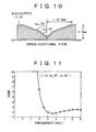
- FIG. 10 illustrates an example of a monoconical antenna whose profile is reduced as compared with optimum half-cone angle constitution.
- the profile is lower than in the optimum half-cone angle constitution.
- a dielectric with a relative dielectric constant ⁇ r of 4 is selected; the height h of the circular cone is set to 6 mm; and the radius r of the base of the circular cone is set to 12.6 mm.
- the half-cone angle is stepped at a midpoint, and the half-cone angle value ⁇ 0 on the base side is set to 70 degrees with the half-cone angle value ⁇ 1 on the vertex side set to 45 degrees.
- the half-cone angle value on the vertex side is made smaller than that on the base side.
- FIG. 11 illustrates the result of a simulation conducted with respect to the VSWR characteristics of a monoconical antenna having the constitution illustrated in FIG. 10. As illustrated in the figure, favorable impedance matching is generally obtained, and a state in which the impedance matching is greatly lost and thus wideband characteristics are lost is avoided. If the combination of half-cone angle values is more finely adjusted, more favorable characteristics would be obtained.
- FIG. 12 illustrates an example of a monoconical antenna whose width is reduced as compared with optimum half-cone angle constitution according to this example.
- the width is smaller than the optimum half-cone angle constitution.
- a dielectric with a relative dielectric constant ⁇ r of 2 is selected; the height h of the circular cone is set to 17.4 mm; and the radius r of the base of the circular cone is set to 9 mm.
- the half-cone angle is stepped at a midpoint, and the half-cone angle value ⁇ 0 on the base side is set to 11 degrees with the half-cone angle value ⁇ 1 on the vertex side is set to 41 degrees.
- the half-cone angle value on the vertex side is made larger than that on the base side.
- FIG. 13 illustrates the result of a simulation conducted with respect to the VSWR characteristics of a monoconical antenna having the constitution illustrated in FIG. 12. As illustrated in the figure, favorable impedance matching is generally obtained.
- FIG. 14 illustrates an example of the constitution of a monoconical antenna provided with a feeding portion structure suitable for mass production.
- a track-like feeding electrode is provided on the base of a dielectric, and the feeding electrode and a radiation electrode are electrically connected with each other through a hole made in the center of the bottom of the dielectric. As illustrated in the figure, this feeding electrode is so formed that its one end reaches the dielectric side face.
- a ground conductor is also formed on the dielectric base. As illustrated in the figure, the ground conductor is so formed that it averts and encircles the feeding electrode. Further, the ground conductor is also so formed that it is extended to the dielectric side face.
- the feeding electrode and ground conductor illustrated in FIG. 14 can be easily formed on the surface of a dielectric by plating, for example. Therefore, use of such a monoconical antenna as illustrated in the figure makes it possible to follow a technique for so-called surface mounting when the antenna is mounted on a circuit board in mass production, and thus the manufacturing process is simplified.
- the body of the monoconical antenna can be fixed on and electrically connected with a circuit board only by soldering the electrodes on the dielectric side face to the electrodes on the circuit board from the surface side.
- the ground conductor need not necessarily be formed on the base of a dielectric, and alternatively, a ground conductor may be formed on the circuit board on which the body of the antenna is to be mounted. In this case, for example, adhesive may be used to fix the body of the antenna.
- the monoconical antennas according to this example illustrated in FIG. 10 and FIG. 12 are so constituted that: when an antenna is reduced in profile or width based on the optimum values of half-cone angle obtained by Expressions (3) and (4) above, deviation of its half-cone angle from the optimum values is compensated. This compensation is carried out by stepping the half-cone angle, and this results in favorable impedance matching.
- FIG. 16 illustrates the cross-sectional structure of a monoconical antenna using low-profile constitution.
- a material with a relative dielectric constant ⁇ r of 4 is used.
- FIG. 17 includes the impedance characteristic diagram and VSWR characteristic diagram of the low-profile monoconical antenna illustrated in FIG. 16. As is evident from the figure, the impedance greatly differs from 50 ohm, and the VSWR characteristics are impaired, especially, in high frequency domain.
- FIG. 18 illustrates the cross-sectional structure of a low-profile monoconical antenna according to the present invention wherein the vertex of the conical radiation electrode is set off the center by 25% with respect to radius.
- the straight line connecting the vertex of the substantially conical radiation electrode and the center of the base of the conical radiation electrode is not perpendicular to the base of the conical radiation electrode.
- FIG. 19 includes the impedance characteristic diagram and VSWR characteristic diagram of the low-profile monoconical antenna illustrated in FIG. 18. As is evident from the figure, the impedance characteristics are close to 50 ohm, and the VSWR characteristics are enhanced as well. Especially, it is important that the lower limit frequency of the matching band is lowered.
- the shape of the concavity formed in one end face of the dielectric is not limited to circular cone. Even if it is formed in the shape of elliptic cone or pyramid, the effect of the present invention is equally produced.
- the definition of its half-cone angle ⁇ is as follows: the average of the minimum angle and the maximum angle among angles formed between the central axis and the side face.
- the dielectric cylinder there is no special limitation on the outside shape of the dielectric cylinder as well. Basically, any shape, including circular cylinder and prism, is acceptable as long as the radiation electrode is covered with it.
- the radiation electrode may be formed by filling it in the conical concavity 11, instead of forming it on the surface of the concavity.
- FIG. 20 illustrates the constitution of the monoconical antenna according to a third example.
- the monoconical antenna comprises: an insulator; a substantially conical concavity provided in one end face of the insulator; a radiation electrode formed on the internal surface of the concavity; a stripped portion obtained by circumferentially stripping part of the radiation electrode; a low-conductivity member filled in the concavity to the level at which at least the stripped portion is buried; and a ground conductor provided in proximity to and substantially in parallel with the other end face of the insulator.
- the substantially conical concavity is provided in the one end face of the insulator.
- the radiation electrode is formed on the internal surface of the concavity by plating or the like. Subsequently, part of the radiation electrode is circumferentially stripped by cutting or the like. Then, the low-conductivity member is filled to the level at which the stripped portion is buried.
- rubber or elastomer containing conductor is suitable for the low-conductivity member. A desired conductivity is obtained with comparative ease by adjusting the conductor content.
- the ground conductor is provided in proximity to and substantially in parallel with the other end face of the insulator. Needless to add, an electrode may be formed as ground conductor directly on the other end face of the insulator.
- the antenna illustrated in FIG. 20 basically functions as a monoconical antenna. By the way, no conductor is present on the upper base of the concavity; however, this does not become a cause of preventing the proper operation of the monoconical antenna. In addition, since the low-conductivity member exists between the two divided radiation electrodes, the electrical effect equivalent to resistive loading is produced.
- FIG. 20 is depicted so that the concavity is formed on the upper side of the insulator.
- the end face provided with the concavity is designated as upper base for convenience in description. However, that does not limit the scope of the present example. (The is the same with the following.))
- FIG. 21 illustrates an example of computation for demonstrating the electrical effect of the monoconical antenna according to this example.
- a VSWR characteristic diagram obtained when the electrode stripped portion is not formed, and on the right is that obtained when the stripped portion is formed. (The other conditions are completely identical.)
- the conditions for the computation will be briefly described below.
- the formation of the electrode stripped portion brings the following advantages: the band wherein VSWR is not more than 2 is expanded to the low-frequency band; the matching property is improved; and band widening of the conical antenna is accomplished.
- one circumferential stripped portion is formed in the radiation electrode formed on the internal surface of the concavity in the insulator.
- the number of the circumferential stripped portions is not limited to one. More specific description will be given. As mentioned above, the presence of the low-conductivity member between the radiation electrodes divided by the stripped portion produces the electrical effect equivalent to resistive loading. For this purpose, two or more circumferential stripped portions may be provided as required.
- FIG. 22 illustrates the constitutions of conical antennas wherein two electrode stripped portions are formed in the direction of the depth of the concavity formed in an insulator.
- the low-conductivity member in the concavity may be provided with multilayer structure as illustrated on the right side of the figure.
- the multilayer structure is such that low-conductivity members different in conductivity are filled level by level at which each electrode stripped portion is buried. At this time, the low-conductivity members are so distributed that the conductivity is lower on the upper base side.
- the effect of diminishing reflective power to the feeding portion is enhanced, and this results in expanded matching band.
- the example is not limited to monoconical antenna, and is effective as a resistive loading method for biconical antenna.
- FIG. 23 illustrates examples wherein the formation of the ground conductor on the other end face of the insulator.
- the resistive loading is applied to biconical antennas formed by disposing radiation electrodes on the internal surfaces of substantially conical concavities symmetrically formed in both the end faces.
- Each of the biconical antennas illustrated in the figure comprises: an insulator; a first substantially conical concavity formed in one end face of the insulator; a first radiation electrode formed on the internal surface of the first concavity; a first stripped portion obtained by circumferentially stripping part of the first radiation electrode; a first low-conductivity member filled in the concavity to the level at which at least the first stripped portion is buried; a second substantially conical concavity formed in the other end face of the insulator; a second radiation electrode formed on the internal surface of the second concavity; a second stripped portion obtained by circumferentially stripping part of the second radiation electrode; and a second low-conductivity member filled in the concavity to the level at which at least the second stripped portion is buried.
- electrical signals are fed to the gap between both the radiation electrodes.
- various methods can be used. For example, parallel lines can be extended from the insulator side face and connected to the vertex regions of both the radiation electrodes. (This method is not shown in the figure.)
- the presence of the low-conductivity member between the radiation electrodes divided by the stripped portion produces the electrical effect equivalent to resistive loading.
- resistive loading is applied to a biconical antenna, this constitution can be similarly adopted. That is, for the above-mentioned purpose, two or more circumferential stripped portions may be provided in each of the upper and lower radiation electrodes as required. (Refer to the center of FIG. 23.)
- the low-conductivity members in the concavities may be provided with multilayer structure.
- the multilayer structure is such that the low-conductivity members different in conductivity are respectively filled to the level at which each electrode stripped portion is buried. At this time, the low-conductivity members are so distributed that the conductivity is lower on the base side. Thus, the effect of diminishing reflective power to the feeding portion is enhanced, and this results in expanded matching band.
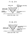
- FIG. 24 illustrates the cross-sectional structure of a monoconical antenna which is a modification to the third example.
- the monoconical antenna illustrated in the figure comprises: an insulator formed in substantially conical shape; a radiation electrode formed on the surface of the substantially conical insulator; a circumferential slit portion which circumferentially divides part of the radiation electrode together with the insulator thereunder; a low-conductivity member filled in the circumferential slit portion; and a ground conductor provided in proximity to the near vertex region of the radiation electrode.
- the radiation electrode is first formed on the surface of the insulator formed in conical shape.
- the radiation electrode can be formed by plating or the like. Subsequently, part of the radiation electrode is circumferentially stripped and cut together with the insulator thereunder by cutting or the like. The thus obtained stripped and cut portion is filled with the low-conductivity member.
- the low-conductivity member rubber or elastomer containing conductor is suitable. A desired conductivity is obtained with comparative ease by adjusting the conductor content. Further, the ground conductor is provided in proximity to the vertex region of the radiation electrode.
- the radiation electrode formed on the surface of the insulator is provided with only one circumferential stripped and cut portion.
- the example does not limit the number of the circumferential stripped and cut portions to one. More specific description will be given. As mentioned above, the presence of the low-conductivity member between the radiation electrodes divided by the stripped portion produces the electrical effect equivalent to resistive loading. For this purpose, two or more circumferential stripped and cut portions may be provide as required.
- FIG. 25 illustrates the constitution of a conical antenna wherein two stripped and cut portions are formed in the direction of the depth of the substantially conical radiation electrode formed on an insulator.
- low-conductivity members different in conductivity may be filled in the individual stripped and cut portions.
- the low-conductivity members are so distributed that the conductivity is lower on the base side of the insulator.
- the effect of diminishing reflective power to the feeding portion is enhanced, and this results in expanded matching band.
- FIG. 24 is not limited to monoconical antenna, and is effective as a resistive loading method for biconical antenna.
- FIG. 26 illustrates examples of the constitutions of biconical antennas using conical antennas which are formed by providing circumferential stripped and cut portions in the radiation electrodes formed on the surfaces of conical insulators.
- Biconical antenna illustrated or the left of FIG. 26 comprises a first insulator formed in substantially conical shape; a first radiation electrode formed on the surface of the substantially conical insulator; a first circumferential slit portion which circumferentially divides part of the first radiation electrode together with the insulator thereunder; a first low-conductivity member filled in the first circumferential slit portion; a second insulator formed in substantially conical shape whose vertex is opposed to that of the first insulator and whose base is symmetrical with that of the first insulator; a second radiation electrode formed on the surface of the substantially conical insulator; a second circumferential slit portion which circumferentially divides part of the second radiation electrode together with the insulator thereunder; and a second low-conductivity member filled in the second circumferential slit portion.
- each insulator As illustrated in FIG. 26, the formation of the ground conductor on the other end face of each insulator in proximity to the near vertex region of the radiation electrode is omitted.
- the conical insulators are so disposed that their respective vertexes are opposed to each other and their respective bases are symmetrical with each other, and the radiation electrode is formed on the surface of each conical insulator.
- Part of each radiation electrode is circumferentially stripped and cut together with the insulator thereunder, and these stripped and cut portions are filled with the low-conductivity member. Needless to add, a support for fixing the disposition of the two conical antennas is required though it is not shown in the figure.
- electrical signals are fed to the gap between both the radiation electrodes.
- various methods can be used. For example, parallel lines can be extended from the insulator side face and connected to the vertex regions of both the radiation electrodes. (This method is not shown in the figure.)
- the present of the low-conductivity member between the radiation electrodes divided by the stripped and cut portion produces the electrical effect equivalent to resistive loading.
- resistive loading according to the example illustrated in FIG. 24 is applied to a biconical antenna, this constitution can be similarly adopted.
- two or more circumferential stripped and cut portions may be provided in each of the upper and lower radiation electrode as required. (Refer to the right side of FIG. 26.)
- low-conductivity members different in conductivity may be filled in the two stripped and cut portions formed in the direction of the depth of the substantially conical radiation electrode formed on each of the upper and lower insulators. At this time, the low-conductivity members are so distributed that the conductivity is lower on the upper base side. Thus, the effect of diminishing reflective power to the feeding portion is enhanced, and this results in expanded matching band.
- FIG. 27 illustrates the cross-sectional structure of a monoconical antenna which is another modification to the third example.
- the monoconical antenna illustrated in the figure comprises: an insulator; a substantially conical concavity provided in one end face of the insulator; a feeding electrode formed on the surface of the near vertex region in the concavity; a low-conductivity member filled in the concavity; and a ground conductor provided in proximity to and substantially in parallel with the other end face of the insulator or formed directly on the other end face of the insulator.
- the conical concavity is first formed in the surface of the insulator, and then the feeding electrode is formed on the internal surface of the concavity in proximity to its vertex.
- the feeding electrode can be formed by plating or the like.
- the concavity is filled with the low-conductivity member.
- rubber or elastomer containing conductor is suitable for the low-conductivity member. A desired conductivity is obtained with comparative ease by adjusting the conductor content.
- the ground conductor is provided in proximity to and substantially in parallel with the other end face of the insulator. Alternatively, the ground conductor may be formed directly on the other end face of the insulator.
- the low-conductivity member functions as a radiation conductor, and further the electrical effect equivalent to resistive loading is obtained.
- the area of the electrode is significantly reduced, and the cost can be accordingly reduced.
- the electrode stripping process is omitted, and the cost can be accordingly reduced.
- FIG. 28 illustrates a modification to the monoconical antenna illustrated in FIG. 27.
- the low-conductivity member filled in the concavity may be provided with multilayer structure wherein members different in conductivity are respectively filled to individual predetermined levels. At this time, the low-conductivity members are so distributed that the conductivity is lower on the upper base side. Thus, the effect of diminishing reflective power to the feeding portion is enhanced, and this results in expanded matching band.
- FIG. 27 is not limited to monoconical antenna, and is effective as a resistive loading method for biconical antenna.
- FIG. 29 illustrates the cross-sectional structure of a biconical antenna constituted using conical antennas which are formed by filling a low-conductivity member in feeding electrodes formed on the surfaces of the conical concavities in an insulator.
- the biconical antenna comprises: a first conical concavity and a second conical concavity symmetrically formed in both the end faces; a first feeding electrode formed on the surface of the near vertex region in the first concavity; a first low-conductivity member filled in the first concavity; a second feeding electrode formed on the surface of the near vertex region in the second concavity; and a second low-conductivity member filled in the second concavity.
- the low-conductivity members function as radiation conductors, and further the electrical effect equivalent to resistive loading is obtained.
- the area of the electrodes is significantly reduced, and the cost can be accordingly reduced.
- the electrode stripping process is omitted, and the cost can be accordingly reduced.
- electrical signals are fed to the gap between the first and second feeding electrodes.
- various methods can be used. For example, parallel lines can be extended from the insulator side face and connected to the vertex regions of both the radiation electrodes. (This method is not shown in the figure.)
- FIG. 30 illustrates an modification to the biconical antenna illustrated in FIG. 29.
- the low-conductivity member filled in each concavity may be provided with multilayer structure wherein members different in conductivity are respectively filled to individual predetermined levels. At this time, the low-conductivity members are so distributed that the conductivity is lower on the upper base side. Thus, the effect of diminishing reflective power to the feeding portion is enhanced, and this results in expanded matching band.
- the radiation electrode of the conical antenna is formed in conical shape.
- the examples are not limited to this, and even if the shape of the radiation electrode is elliptic cone or pyramid, the effect is equally produced.
- the outside shape of the insulator cylinder either and basically, any shape, including circular cylinder and prism, easy to handle may be adopted.
- the insulator is not limited to dielectric, and even a magnetic material does not have influence on the essential effect of the examples.
- an excellent monoconical antenna wherein reduction in profile and width is accomplished regardless of the selection of dielectric can be provided.
- the thus obtained antenna is useful, for example, as a small, low-profile antenna or small, slender antenna for ultra-wide band communication system.
Landscapes
- Details Of Aerials (AREA)
- Waveguide Aerials (AREA)
Claims (2)
- Monokonusantenne (1) mit einer konischen Strahlungselektrode (12), die einen Scheitelpunkt (14) und eine Grundfläche aufweist,
und mit einem Erdleiter (13), der in der Nähe der betreffenden Strahlungselektrode (12) vorgesehen ist und der parallel zu der Grundfläche der konischen Strahlungselektrode (12) verläuft,
wobei die betreffende Antenne (1) so aufgebaut ist, dass elektrische Signale zwischen einem Nah-Scheitelpunktbereich (14) der genannten Strahlungselektrode (12) und einem Bereich des genannten Erdleiters (13) zugeführt werden,
dadurch gekennzeichnet, dass eine den genannten Scheitelpunkt (14) der konischen Strahlungselektrode (12) und die Mitte der Grundfläche der konischen Strahlungselektrode (12) verbindende gerade Linie nicht rechtwinklig zu der Grundfläche der konischen Strahlungselektrode (12) verläuft. - Monokonusantenne nach Anspruch 1, wobei zwischen die genannte Strahlungselektrode (12) und den genannten Erdleiter (13) ein Dielektrikum (10) eingefüllt ist.
Applications Claiming Priority (13)
| Application Number | Priority Date | Filing Date | Title |
|---|---|---|---|
| JP2002307908 | 2002-10-23 | ||
| JP2002307909 | 2002-10-23 | ||
| JP2002307908 | 2002-10-23 | ||
| JP2002307909 | 2002-10-23 | ||
| JP2002315381 | 2002-10-30 | ||
| JP2002315381 | 2002-10-30 | ||
| JP2003049895 | 2003-02-26 | ||
| JP2003049896 | 2003-02-26 | ||
| JP2003049895A JP3649224B2 (ja) | 2002-10-23 | 2003-02-26 | モノコニカル・アンテナ |
| JP2003049896 | 2003-02-26 | ||
| JP2003096903A JP4033022B2 (ja) | 2002-10-23 | 2003-03-31 | コニカル・アンテナ及びその製造方法 |
| JP2003096903 | 2003-03-31 | ||
| EP03758778A EP1555719B1 (de) | 2002-10-23 | 2003-10-22 | Breitbandantenne |
Related Parent Applications (2)
| Application Number | Title | Priority Date | Filing Date |
|---|---|---|---|
| EP03758778A Division EP1555719B1 (de) | 2002-10-23 | 2003-10-22 | Breitbandantenne |
| EP03758778.9 Division | 2003-10-22 |
Publications (3)
| Publication Number | Publication Date |
|---|---|
| EP1585193A2 EP1585193A2 (de) | 2005-10-12 |
| EP1585193A3 EP1585193A3 (de) | 2006-03-15 |
| EP1585193B1 true EP1585193B1 (de) | 2008-01-09 |
Family
ID=32180812
Family Applications (5)
| Application Number | Title | Priority Date | Filing Date |
|---|---|---|---|
| EP03758778A Expired - Lifetime EP1555719B1 (de) | 2002-10-23 | 2003-10-22 | Breitbandantenne |
| EP08013167A Expired - Lifetime EP2001083B1 (de) | 2002-10-23 | 2003-10-22 | Breitbandantenne |
| EP08013166A Withdrawn EP2001082A3 (de) | 2002-10-23 | 2003-10-22 | Breitbandantenne |
| EP05027200A Expired - Lifetime EP1648051B1 (de) | 2002-10-23 | 2003-10-22 | Breitbandantenne |
| EP05012924A Expired - Lifetime EP1585193B1 (de) | 2002-10-23 | 2003-10-22 | Breitbandantenne |
Family Applications Before (4)
| Application Number | Title | Priority Date | Filing Date |
|---|---|---|---|
| EP03758778A Expired - Lifetime EP1555719B1 (de) | 2002-10-23 | 2003-10-22 | Breitbandantenne |
| EP08013167A Expired - Lifetime EP2001083B1 (de) | 2002-10-23 | 2003-10-22 | Breitbandantenne |
| EP08013166A Withdrawn EP2001082A3 (de) | 2002-10-23 | 2003-10-22 | Breitbandantenne |
| EP05027200A Expired - Lifetime EP1648051B1 (de) | 2002-10-23 | 2003-10-22 | Breitbandantenne |
Country Status (9)
| Country | Link |
|---|---|
| US (3) | US7132993B2 (de) |
| EP (5) | EP1555719B1 (de) |
| KR (1) | KR101077793B1 (de) |
| CN (2) | CN1685562B (de) |
| AU (1) | AU2003275586A1 (de) |
| DE (4) | DE60328619D1 (de) |
| ES (3) | ES2326970T3 (de) |
| MX (1) | MXPA04005983A (de) |
| WO (1) | WO2004038861A1 (de) |
Families Citing this family (30)
| Publication number | Priority date | Publication date | Assignee | Title |
|---|---|---|---|---|
| DE60328619D1 (de) * | 2002-10-23 | 2009-09-10 | Sony Corp | Breitbandantenne |
| US7006047B2 (en) * | 2003-01-24 | 2006-02-28 | Bae Systems Information And Electronic Systems Integration Inc. | Compact low RCS ultra-wide bandwidth conical monopole antenna |
| US7456799B1 (en) | 2003-03-29 | 2008-11-25 | Fractal Antenna Systems, Inc. | Wideband vehicular antennas |
| US7190318B2 (en) * | 2003-03-29 | 2007-03-13 | Nathan Cohen | Wide-band fractal antenna |
| US7444734B2 (en) * | 2003-12-09 | 2008-11-04 | International Business Machines Corporation | Apparatus and methods for constructing antennas using vias as radiating elements formed in a substrate |
| JP4475583B2 (ja) * | 2004-07-13 | 2010-06-09 | 株式会社リコー | ディスコーンアンテナおよび該ディスコーンアンテナを用いた情報通信機器 |
| US20070241982A1 (en) * | 2004-09-30 | 2007-10-18 | Alan Stigliani | Contoured triangular dipole antenna |
| FR2883671A1 (fr) * | 2005-03-24 | 2006-09-29 | Groupe Ecoles Telecomm | Antenne ultra-large bande offrant une grande flexibilite de conception |
| DE102005022493A1 (de) * | 2005-05-11 | 2006-11-16 | Endress + Hauser Gmbh + Co. Kg | Vorrichtung zur Ermittlung und Überwachung des Füllstandes eines Mediums in einem Behälter |
| US7286095B2 (en) * | 2005-06-20 | 2007-10-23 | Harris Corporation | Inverted feed discone antenna and related methods |
| DE502005003107D1 (de) * | 2005-08-11 | 2008-04-17 | Festo Ag & Co | Abstandsmessvorrichtung mit einer Mikrowellen-Antennenanordnung und Verfahren zu ihrer Herstellung |
| US7872607B2 (en) * | 2006-01-27 | 2011-01-18 | Qualcomm, Incorporated | Diverse spectrum antenna for handsets and other devices |
| US7940225B1 (en) * | 2007-06-19 | 2011-05-10 | The United States Of America As Represented By The Secretary Of The Navy | Antenna with shaped dielectric loading |
| US7791554B2 (en) * | 2008-07-25 | 2010-09-07 | The United States Of America As Represented By The Attorney General | Tulip antenna with tuning stub |
| GB0903514D0 (en) * | 2009-02-28 | 2009-04-08 | Original Perspectives Ltd | Hyperband antenna arm and antenna |
| US9343798B2 (en) * | 2011-09-26 | 2016-05-17 | Gary Gwoon Wong | High performance (mini-cube) indoor HDTV antenna |
| CN103117451B (zh) * | 2013-03-04 | 2016-03-02 | 金明涛 | 超宽带天线 |
| US9634396B2 (en) * | 2013-07-09 | 2017-04-25 | Galtronics Corporation Ltd. | Extremely low-profile antenna |
| US9847571B2 (en) * | 2013-11-06 | 2017-12-19 | Symbol Technologies, Llc | Compact, multi-port, MIMO antenna with high port isolation and low pattern correlation and method of making same |
| US10158178B2 (en) | 2013-11-06 | 2018-12-18 | Symbol Technologies, Llc | Low profile, antenna array for an RFID reader and method of making same |
| US9553369B2 (en) * | 2014-02-07 | 2017-01-24 | Her Majesty The Queen In Right Of Canada, As Represented By The Minister Of National Defence | Ultra-wideband biconical antenna with excellent gain and impedance matching |
| US20160043472A1 (en) * | 2014-04-28 | 2016-02-11 | Tyco Electronics Corporation | Monocone antenna |
| US9692136B2 (en) * | 2014-04-28 | 2017-06-27 | Te Connectivity Corporation | Monocone antenna |
| AU2016367704A1 (en) * | 2015-12-09 | 2018-04-19 | Licensys Australasia Pty Ltd | An antenna |
| KR101893555B1 (ko) | 2017-08-21 | 2018-08-30 | 국방과학연구소 | 안테나 장치 |
| JP2019047328A (ja) * | 2017-09-01 | 2019-03-22 | 富士通株式会社 | アンテナ及び通信装置 |
| US12003023B2 (en) * | 2019-01-26 | 2024-06-04 | Intel Corporation | In-package 3D antenna |
| US11038278B2 (en) * | 2019-08-15 | 2021-06-15 | United States Of America As Represented By The Secretary Of The Navy | Lens apparatus and methods for an antenna |
| US20220336946A1 (en) * | 2019-09-05 | 2022-10-20 | Lg Electronics Inc. | Electronic device having antenna |
| WO2024192431A1 (en) * | 2023-03-16 | 2024-09-19 | Massive Light, LLC | Ultra-wideband, low-distortion, omni-directional, and placement-insensitive antennas |
Family Cites Families (27)
| Publication number | Priority date | Publication date | Assignee | Title |
|---|---|---|---|---|
| US3401387A (en) * | 1966-02-16 | 1968-09-10 | Northrop Corp | Slotted cone antenna |
| CA1055600A (en) | 1976-03-05 | 1979-05-29 | Michael Hamid | Wideband antenna |
| US4074268A (en) * | 1976-06-21 | 1978-02-14 | Hoffman Electronics Corporation | Electronically scanned antenna |
| FR2372522A1 (fr) * | 1976-11-30 | 1978-06-23 | Thomson Csf | Antenne omnidirectionnelle a diagramme de directivite reglable en site |
| JPS53129251A (en) | 1977-04-19 | 1978-11-11 | Toshiba Machine Co Ltd | Multilayer die for sheet forming |
| GB2164517B (en) * | 1984-02-29 | 1988-02-17 | Thomas Michael Benyon Wright | Improvements to antenna systems |
| JPS645203U (de) | 1987-06-29 | 1989-01-12 | ||
| JPH0821595B2 (ja) | 1987-07-28 | 1996-03-04 | 三菱電機株式会社 | 半導体装置 |
| US4851859A (en) * | 1988-05-06 | 1989-07-25 | Purdue Research Foundation | Tunable discone antenna |
| US4947181A (en) * | 1988-12-19 | 1990-08-07 | Raytheon Company | Asymmetrical biconical horn antenna |
| JPH02246502A (ja) | 1989-02-18 | 1990-10-02 | Du Pont Japan Ltd | アンテナ |
| JPH02270405A (ja) * | 1989-04-12 | 1990-11-05 | Nissan Motor Co Ltd | 平板パッチアンテナ |
| JPH02298105A (ja) * | 1989-05-11 | 1990-12-10 | Murata Mfg Co Ltd | マイクロストリップ・アンテナ |
| US5038152A (en) * | 1990-05-17 | 1991-08-06 | Hughes Aircraft Company | Broad band omnidirectional monocone antenna |
| US5506592A (en) * | 1992-05-29 | 1996-04-09 | Texas Instruments Incorporated | Multi-octave, low profile, full instantaneous azimuthal field of view direction finding antenna |
| JPH08139515A (ja) | 1994-11-11 | 1996-05-31 | Toko Inc | 誘電体垂直偏波アンテナ |
| JP2733451B2 (ja) * | 1994-11-16 | 1998-03-30 | 日東工業株式会社 | 配線用遮断器 |
| JPH09153727A (ja) | 1995-11-29 | 1997-06-10 | Furukawa C & B Kk | 広帯域アンテナ |
| IT1319430B1 (it) * | 2000-09-13 | 2003-10-10 | Zendar Spa | Antenna a basso profilo, senza stilo |
| US6661389B2 (en) * | 2000-11-20 | 2003-12-09 | Vega Grieshaber Kg | Horn antenna for a radar device |
| US6956534B2 (en) * | 2000-12-27 | 2005-10-18 | Cocomo Mb Communications, Inc. | Method and apparatus for improving antenna efficiency |
| JP2002298105A (ja) | 2001-03-30 | 2002-10-11 | Sony Corp | データ記憶装置および方法、情報処理装置および方法、記録媒体、並びにプログラム |
| US6697031B2 (en) * | 2001-08-01 | 2004-02-24 | Lucent Technologies Inc | Antenna |
| DE60328619D1 (de) * | 2002-10-23 | 2009-09-10 | Sony Corp | Breitbandantenne |
| US7215294B2 (en) * | 2003-05-23 | 2007-05-08 | Lucent Technologies Inc. | Antenna with reflector |
| JP4234617B2 (ja) * | 2004-01-30 | 2009-03-04 | 富士通コンポーネント株式会社 | アンテナ装置 |
| JP4280182B2 (ja) * | 2004-03-09 | 2009-06-17 | 富士通コンポーネント株式会社 | アンテナ装置 |
-
2003
- 2003-10-22 DE DE60328619T patent/DE60328619D1/de not_active Expired - Lifetime
- 2003-10-22 KR KR1020047009973A patent/KR101077793B1/ko not_active IP Right Cessation
- 2003-10-22 EP EP03758778A patent/EP1555719B1/de not_active Expired - Lifetime
- 2003-10-22 DE DE60323406T patent/DE60323406D1/de not_active Expired - Lifetime
- 2003-10-22 DE DE60336865T patent/DE60336865D1/de not_active Expired - Lifetime
- 2003-10-22 CN CN2003801000901A patent/CN1685562B/zh not_active Expired - Fee Related
- 2003-10-22 EP EP08013167A patent/EP2001083B1/de not_active Expired - Lifetime
- 2003-10-22 US US10/498,813 patent/US7132993B2/en not_active Expired - Fee Related
- 2003-10-22 ES ES03758778T patent/ES2326970T3/es not_active Expired - Lifetime
- 2003-10-22 EP EP08013166A patent/EP2001082A3/de not_active Withdrawn
- 2003-10-22 DE DE60318626T patent/DE60318626T2/de not_active Expired - Lifetime
- 2003-10-22 EP EP05027200A patent/EP1648051B1/de not_active Expired - Lifetime
- 2003-10-22 EP EP05012924A patent/EP1585193B1/de not_active Expired - Lifetime
- 2003-10-22 AU AU2003275586A patent/AU2003275586A1/en not_active Abandoned
- 2003-10-22 ES ES05027200T patent/ES2314548T3/es not_active Expired - Lifetime
- 2003-10-22 WO PCT/JP2003/013487 patent/WO2004038861A1/ja active Application Filing
- 2003-10-22 CN CN2008100874024A patent/CN101246995B/zh not_active Expired - Fee Related
- 2003-10-22 ES ES05012924T patent/ES2297565T3/es not_active Expired - Lifetime
-
2004
- 2004-06-18 MX MXPA04005983A patent/MXPA04005983A/es active IP Right Grant
-
2006
- 2006-07-19 US US11/488,678 patent/US7352334B2/en not_active Expired - Fee Related
- 2006-07-19 US US11/488,753 patent/US7626558B2/en not_active Expired - Fee Related
Also Published As
Similar Documents
| Publication | Publication Date | Title |
|---|---|---|
| EP1585193B1 (de) | Breitbandantenne | |
| EP2297817B1 (de) | Geklappte konische antenne und diesbezügliche verfahren | |
| US6624788B2 (en) | Antenna arrangement | |
| EP1551079A1 (de) | Miniaturisierte Ultrabreitband-Mikrostreifenantenne | |
| US6590543B1 (en) | Double monopole meanderline loaded antenna | |
| US8917216B2 (en) | Antenna device with U-shaped slit | |
| DE19729664C2 (de) | Planare Breitbandantenne | |
| US6788265B2 (en) | Antenna element | |
| Cho et al. | Bidirectional rod antenna composed of narrow patches | |
| JPH08250925A (ja) | 広帯域線状アンテナ | |
| Mohamed | Design of Efficient Millimeter Waves Planar Antennas For 5G Communication Systems | |
| CN113097696A (zh) | 超宽带天线 | |
| JP4214887B2 (ja) | モノコニカル・アンテナ | |
| CN216872250U (zh) | 紧凑型宽带新月形贴片对天线 | |
| JP4033022B2 (ja) | コニカル・アンテナ及びその製造方法 | |
| JP5280973B2 (ja) | アンテナ | |
| Greenberg et al. | Characterization of bunny-ear antennas for wireless basestation applications | |
| ES2365439T3 (es) | Antena de banda ancha. |
Legal Events
| Date | Code | Title | Description |
|---|---|---|---|
| PUAI | Public reference made under article 153(3) epc to a published international application that has entered the european phase |
Free format text: ORIGINAL CODE: 0009012 |
|
| 17P | Request for examination filed |
Effective date: 20050615 |
|
| AC | Divisional application: reference to earlier application |
Ref document number: 1555719 Country of ref document: EP Kind code of ref document: P |
|
| AK | Designated contracting states |
Kind code of ref document: A2 Designated state(s): AT BE BG CH CY CZ DE DK EE ES FI FR GB GR HU IE IT LI LU MC NL PT RO SE SI SK TR |
|
| PUAL | Search report despatched |
Free format text: ORIGINAL CODE: 0009013 |
|
| AK | Designated contracting states |
Kind code of ref document: A3 Designated state(s): AT BE BG CH CY CZ DE DK EE ES FI FR GB GR HU IE IT LI LU MC NL PT RO SE SI SK TR |
|
| AKX | Designation fees paid |
Designated state(s): DE ES FR GB |
|
| 17Q | First examination report despatched |
Effective date: 20061103 |
|
| GRAP | Despatch of communication of intention to grant a patent |
Free format text: ORIGINAL CODE: EPIDOSNIGR1 |
|
| GRAS | Grant fee paid |
Free format text: ORIGINAL CODE: EPIDOSNIGR3 |
|
| GRAA | (expected) grant |
Free format text: ORIGINAL CODE: 0009210 |
|
| AC | Divisional application: reference to earlier application |
Ref document number: 1555719 Country of ref document: EP Kind code of ref document: P |
|
| AK | Designated contracting states |
Kind code of ref document: B1 Designated state(s): DE ES FR GB |
|
| REG | Reference to a national code |
Ref country code: GB Ref legal event code: FG4D |
|
| REF | Corresponds to: |
Ref document number: 60318626 Country of ref document: DE Date of ref document: 20080221 Kind code of ref document: P |
|
| REG | Reference to a national code |
Ref country code: ES Ref legal event code: FG2A Ref document number: 2297565 Country of ref document: ES Kind code of ref document: T3 |
|
| ET | Fr: translation filed | ||
| PLBE | No opposition filed within time limit |
Free format text: ORIGINAL CODE: 0009261 |
|
| STAA | Information on the status of an ep patent application or granted ep patent |
Free format text: STATUS: NO OPPOSITION FILED WITHIN TIME LIMIT |
|
| 26N | No opposition filed |
Effective date: 20081010 |
|
| REG | Reference to a national code |
Ref country code: GB Ref legal event code: 746 Effective date: 20091130 |
|
| PGFP | Annual fee paid to national office [announced via postgrant information from national office to epo] |
Ref country code: FR Payment date: 20101104 Year of fee payment: 8 |
|
| PGFP | Annual fee paid to national office [announced via postgrant information from national office to epo] |
Ref country code: DE Payment date: 20101022 Year of fee payment: 8 |
|
| PGFP | Annual fee paid to national office [announced via postgrant information from national office to epo] |
Ref country code: GB Payment date: 20101021 Year of fee payment: 8 |
|
| PGFP | Annual fee paid to national office [announced via postgrant information from national office to epo] |
Ref country code: ES Payment date: 20101021 Year of fee payment: 8 |
|
| GBPC | Gb: european patent ceased through non-payment of renewal fee |
Effective date: 20111022 |
|
| REG | Reference to a national code |
Ref country code: FR Ref legal event code: ST Effective date: 20120629 |
|
| PG25 | Lapsed in a contracting state [announced via postgrant information from national office to epo] |
Ref country code: DE Free format text: LAPSE BECAUSE OF NON-PAYMENT OF DUE FEES Effective date: 20120501 |
|
| PG25 | Lapsed in a contracting state [announced via postgrant information from national office to epo] |
Ref country code: GB Free format text: LAPSE BECAUSE OF NON-PAYMENT OF DUE FEES Effective date: 20111022 Ref country code: FR Free format text: LAPSE BECAUSE OF NON-PAYMENT OF DUE FEES Effective date: 20111102 |
|
| REG | Reference to a national code |
Ref country code: DE Ref legal event code: R119 Ref document number: 60318626 Country of ref document: DE Effective date: 20120501 |
|
| REG | Reference to a national code |
Ref country code: ES Ref legal event code: FD2A Effective date: 20130417 |
|
| PG25 | Lapsed in a contracting state [announced via postgrant information from national office to epo] |
Ref country code: ES Free format text: LAPSE BECAUSE OF NON-PAYMENT OF DUE FEES Effective date: 20111023 |