EP1585115A2 - Data recording apparatus - Google Patents
Data recording apparatus Download PDFInfo
- Publication number
- EP1585115A2 EP1585115A2 EP05012117A EP05012117A EP1585115A2 EP 1585115 A2 EP1585115 A2 EP 1585115A2 EP 05012117 A EP05012117 A EP 05012117A EP 05012117 A EP05012117 A EP 05012117A EP 1585115 A2 EP1585115 A2 EP 1585115A2
- Authority
- EP
- European Patent Office
- Prior art keywords
- lowpass filter
- data recording
- signal
- sampling
- laser diode
- Prior art date
- Legal status (The legal status is an assumption and is not a legal conclusion. Google has not performed a legal analysis and makes no representation as to the accuracy of the status listed.)
- Granted
Links
Images


Classifications
-
- G—PHYSICS
- G11—INFORMATION STORAGE
- G11B—INFORMATION STORAGE BASED ON RELATIVE MOVEMENT BETWEEN RECORD CARRIER AND TRANSDUCER
- G11B7/00—Recording or reproducing by optical means, e.g. recording using a thermal beam of optical radiation by modifying optical properties or the physical structure, reproducing using an optical beam at lower power by sensing optical properties; Record carriers therefor
- G11B7/004—Recording, reproducing or erasing methods; Read, write or erase circuits therefor
- G11B7/006—Overwriting
- G11B7/0062—Overwriting strategies, e.g. recording pulse sequences with erasing level used for phase-change media
-
- G—PHYSICS
- G11—INFORMATION STORAGE
- G11B—INFORMATION STORAGE BASED ON RELATIVE MOVEMENT BETWEEN RECORD CARRIER AND TRANSDUCER
- G11B7/00—Recording or reproducing by optical means, e.g. recording using a thermal beam of optical radiation by modifying optical properties or the physical structure, reproducing using an optical beam at lower power by sensing optical properties; Record carriers therefor
- G11B7/12—Heads, e.g. forming of the optical beam spot or modulation of the optical beam
- G11B7/125—Optical beam sources therefor, e.g. laser control circuitry specially adapted for optical storage devices; Modulators, e.g. means for controlling the size or intensity of optical spots or optical traces
- G11B7/126—Circuits, methods or arrangements for laser control or stabilisation
- G11B7/1263—Power control during transducing, e.g. by monitoring
-
- G—PHYSICS
- G11—INFORMATION STORAGE
- G11B—INFORMATION STORAGE BASED ON RELATIVE MOVEMENT BETWEEN RECORD CARRIER AND TRANSDUCER
- G11B7/00—Recording or reproducing by optical means, e.g. recording using a thermal beam of optical radiation by modifying optical properties or the physical structure, reproducing using an optical beam at lower power by sensing optical properties; Record carriers therefor
- G11B7/004—Recording, reproducing or erasing methods; Read, write or erase circuits therefor
- G11B7/0045—Recording
- G11B7/00456—Recording strategies, e.g. pulse sequences
Definitions
- the latter another method does not reduce the accuracy of light intensity because the peak hold capability can be used to perform feedback control.
- the circuit for peak hold has a large scale.
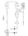
- the switch 7 is constantly in the on-state, and the lowpass filter 2 is set at the non-operation state with the output of the lowpass filter 2 being consistent with the signal level (-V 1 ) obtained when laser light with the read level of RL is applied.
- the lowpass filter 2 is operated only during the time period over which the record mark with the length of 14T, whereby only the detection signal of the front monitor diode FMD during this time period is extracted, thus making it possible to detect correctly and control the intensity of light emitted from the laser diode LD.
- the lowpass filter 2 is operated only when the record mark with the length of 14T is written, and therefore the luminous intensity of the laser diode LD can be reflected correctly in the output signal of the lowpass filter 2.
- the luminous intensity of the laser diode LD can be controlled with high accuracy.
- circuits for peak holding and the like are not required, and therefore the scale of the circuit can be reduced, thus making it possible to reduce cost for assembling the device.
Landscapes
- Physics & Mathematics (AREA)
- Optics & Photonics (AREA)
- Optical Recording Or Reproduction (AREA)
- Optical Head (AREA)
Abstract
Description
a band switching device for switching the filter band of said lowpass filter according to the data recording rate to record the data for said data recording medium.
Claims (3)
- A data recording apparatus comprising:a photoirradiation device (LD) for applying a light to a data recording medium to record data;a detection device (FMD) for detecting the intensity of light emitted from said photoirradiation device (LD);a lowpass filter (2) for receiving a signal which is output from said detection device (FMD);a sampling device (3) for sampling a signal which is output from said lowpass filter (2);a control device (6) for controlling the intensity of light emitted from said photoirradiation device (LD) based on the signal sampled by said sampling device (3); anda sampling timing switching device (8) for switching the sampling timing of said sampling device (3) according to the data recording rate to record the data for said data recording medium.
- The data recording apparatus according to claim 1, comprising:a band switching device (9) for switching the filter band of said lowpass filter (2) according to the data recording rate to record the data for said data recording medium.
- The data recording apparatus according to any of claims 1 to 2, wherein:said sampling device (3) samples the signal which is output from said lowpass filter (2) at a point of time before the signal which is output from said lowpass filter (2) converges to a predetermined level.
Applications Claiming Priority (5)
| Application Number | Priority Date | Filing Date | Title |
|---|---|---|---|
| JP2001304910 | 2001-10-01 | ||
| JP2001304910 | 2001-10-01 | ||
| JP2002044222 | 2002-02-21 | ||
| JP2002044222 | 2002-02-21 | ||
| EP02256238A EP1298649B1 (en) | 2001-10-01 | 2002-09-10 | Data recording apparatus |
Related Parent Applications (1)
| Application Number | Title | Priority Date | Filing Date |
|---|---|---|---|
| EP02256238A Division EP1298649B1 (en) | 2001-10-01 | 2002-09-10 | Data recording apparatus |
Publications (3)
| Publication Number | Publication Date |
|---|---|
| EP1585115A2 true EP1585115A2 (en) | 2005-10-12 |
| EP1585115A3 EP1585115A3 (en) | 2005-10-19 |
| EP1585115B1 EP1585115B1 (en) | 2006-11-02 |
Family
ID=26623510
Family Applications (3)
| Application Number | Title | Priority Date | Filing Date |
|---|---|---|---|
| EP05012116A Withdrawn EP1585114A1 (en) | 2001-10-01 | 2002-09-10 | Data recording apparatus |
| EP05012117A Expired - Lifetime EP1585115B1 (en) | 2001-10-01 | 2002-09-10 | Data recording apparatus |
| EP02256238A Expired - Lifetime EP1298649B1 (en) | 2001-10-01 | 2002-09-10 | Data recording apparatus |
Family Applications Before (1)
| Application Number | Title | Priority Date | Filing Date |
|---|---|---|---|
| EP05012116A Withdrawn EP1585114A1 (en) | 2001-10-01 | 2002-09-10 | Data recording apparatus |
Family Applications After (1)
| Application Number | Title | Priority Date | Filing Date |
|---|---|---|---|
| EP02256238A Expired - Lifetime EP1298649B1 (en) | 2001-10-01 | 2002-09-10 | Data recording apparatus |
Country Status (5)
| Country | Link |
|---|---|
| US (1) | US6822210B2 (en) |
| EP (3) | EP1585114A1 (en) |
| KR (1) | KR100545320B1 (en) |
| CN (1) | CN1180409C (en) |
| DE (2) | DE60207354T2 (en) |
Families Citing this family (5)
| Publication number | Priority date | Publication date | Assignee | Title |
|---|---|---|---|---|
| TWI303061B (en) * | 2004-02-19 | 2008-11-11 | Mediatek Inc | Optical pickup capable of reducing signal distortion and signal processing method thereof |
| JP2005353133A (en) * | 2004-06-09 | 2005-12-22 | Hitachi Ltd | Method of deriving appropriate sample-and-hold timing, and optical disk apparatus using this method |
| TW200746626A (en) * | 2006-06-05 | 2007-12-16 | Mediatek Inc | High pass filtering device and servo control apparatus of an optical disc drive |
| CN101105954B (en) * | 2006-07-14 | 2012-08-29 | 鸿富锦精密工业(深圳)有限公司 | Writing capability correction method and information recording device |
| US20080084805A1 (en) * | 2006-10-05 | 2008-04-10 | Hon Hai Precision Industry Co., Ltd. | Writing power calibrating method and data recording apparatus using the same |
Family Cites Families (14)
| Publication number | Priority date | Publication date | Assignee | Title |
|---|---|---|---|---|
| JPH07111782B2 (en) * | 1986-08-13 | 1995-11-29 | ソニー株式会社 | Optical disc recording / reproducing device |
| JPH0827958B2 (en) * | 1988-09-16 | 1996-03-21 | パイオニア株式会社 | Optical power control device for semiconductor light emitting element |
| EP0388833B1 (en) * | 1989-03-20 | 1996-06-19 | Hitachi, Ltd. | Optical recording system |
| JPH03136101A (en) * | 1989-10-23 | 1991-06-10 | Olympus Optical Co Ltd | Digital servo-device |
| JPH0521883A (en) | 1991-07-11 | 1993-01-29 | Pioneer Electron Corp | Output control device |
| KR930014352A (en) * | 1991-12-31 | 1993-07-23 | 정용문 | Laser light quantity control circuit in optical drive system |
| US5537383A (en) * | 1995-03-01 | 1996-07-16 | Eastman Kodak Company | Optical data storage system with differential data detection and source noise subtraction for use with magneto-optic, write-once and other optical media |
| JPH0922530A (en) * | 1995-07-03 | 1997-01-21 | Ricoh Co Ltd | Optical output setting method for information recording / playback |
| JP3096239B2 (en) * | 1996-04-01 | 2000-10-10 | 太陽誘電株式会社 | Optical disc running OPC method and optical disc recording / reproducing apparatus |
| JP2000021001A (en) | 1998-06-30 | 2000-01-21 | Pioneer Electron Corp | Optical pickup device |
| JP4068752B2 (en) * | 1999-03-02 | 2008-03-26 | シャープ株式会社 | Optical disk device |
| US6490302B1 (en) * | 1999-10-28 | 2002-12-03 | Matsushita Electric Industrial Co., Ltd. | Semiconductor laser control circuit and laser light source |
| JP2002100044A (en) * | 2000-09-25 | 2002-04-05 | Sony Corp | Optical recording apparatus and laser power control method therefor |
| JP3814476B2 (en) * | 2000-09-28 | 2006-08-30 | 日本ビクター株式会社 | Information recording method and information recording apparatus |
-
2002
- 2002-09-10 DE DE60207354T patent/DE60207354T2/en not_active Expired - Fee Related
- 2002-09-10 EP EP05012116A patent/EP1585114A1/en not_active Withdrawn
- 2002-09-10 DE DE60215870T patent/DE60215870T2/en not_active Expired - Fee Related
- 2002-09-10 EP EP05012117A patent/EP1585115B1/en not_active Expired - Lifetime
- 2002-09-10 EP EP02256238A patent/EP1298649B1/en not_active Expired - Lifetime
- 2002-09-24 US US10/252,571 patent/US6822210B2/en not_active Expired - Fee Related
- 2002-09-27 KR KR1020020058864A patent/KR100545320B1/en not_active Expired - Fee Related
- 2002-09-29 CN CNB02144255XA patent/CN1180409C/en not_active Expired - Fee Related
Also Published As
| Publication number | Publication date |
|---|---|
| DE60215870D1 (en) | 2006-12-14 |
| US6822210B2 (en) | 2004-11-23 |
| DE60207354D1 (en) | 2005-12-22 |
| CN1180409C (en) | 2004-12-15 |
| EP1585115A3 (en) | 2005-10-19 |
| DE60207354T2 (en) | 2006-06-01 |
| US20030062466A1 (en) | 2003-04-03 |
| DE60215870T2 (en) | 2007-03-08 |
| KR100545320B1 (en) | 2006-01-24 |
| EP1298649A3 (en) | 2004-03-24 |
| EP1585115B1 (en) | 2006-11-02 |
| EP1585114A1 (en) | 2005-10-12 |
| EP1298649A2 (en) | 2003-04-02 |
| CN1409307A (en) | 2003-04-09 |
| KR20030028409A (en) | 2003-04-08 |
| EP1298649B1 (en) | 2005-11-16 |
Similar Documents
| Publication | Publication Date | Title |
|---|---|---|
| KR910003460B1 (en) | Optical information-recording apparatus | |
| KR100606255B1 (en) | Information recording apparatus | |
| EP1136992A2 (en) | Apparatus and method for controlling auto laser diode power | |
| JP2000216470A (en) | Laser drive device and optical disk recording / reproducing device | |
| JPH11144288A (en) | Laser power control method for optical disk recording and laser diode driving circuit for optical disk recorder | |
| EP1298649B1 (en) | Data recording apparatus | |
| JP3257287B2 (en) | Optical disk recording device | |
| JPH1166594A (en) | Optical disc recorder | |
| KR100493033B1 (en) | Laser power controlling device | |
| JP3800534B2 (en) | Information recording device | |
| EP1515314A1 (en) | Information recording device and information recording method | |
| JP2003077128A (en) | Information recording device and information recording method | |
| KR100363173B1 (en) | Auto output control apparatus of laser diode | |
| JPH11144287A (en) | Optical disk recorder | |
| JP4347771B2 (en) | Apparatus and method for controlling laser diode power in optical drive | |
| JP3187594B2 (en) | Optical information recording / reproducing device | |
| JP4406348B2 (en) | Voltage level detection apparatus and method, and laser output control apparatus and method | |
| CN100487798C (en) | Recording pulse generating apparatus and information recording apparatus | |
| JP2002150591A (en) | Recorder by optical recording medium and its recording method | |
| JP4086650B2 (en) | Optical disc apparatus and method for controlling optical disc apparatus | |
| JPWO2005041175A1 (en) | Information recording device and information recording method | |
| JPH11134692A (en) | Optical disk recorder | |
| KR20080081012A (en) | Optical recording device with high speed forward laser power control (LPC) | |
| JPH09161302A (en) | Circuit and method for controlling semiconductor laser | |
| JP2000048387A (en) | Method and circuit for writing compensation and optical disk recording device |
Legal Events
| Date | Code | Title | Description |
|---|---|---|---|
| PUAI | Public reference made under article 153(3) epc to a published international application that has entered the european phase |
Free format text: ORIGINAL CODE: 0009012 |
|
| PUAL | Search report despatched |
Free format text: ORIGINAL CODE: 0009013 |
|
| AC | Divisional application: reference to earlier application |
Ref document number: 1298649 Country of ref document: EP Kind code of ref document: P |
|
| AK | Designated contracting states |
Kind code of ref document: A2 Designated state(s): DE FR GB |
|
| AK | Designated contracting states |
Kind code of ref document: A3 Designated state(s): DE FR GB |
|
| 17P | Request for examination filed |
Effective date: 20051031 |
|
| GRAP | Despatch of communication of intention to grant a patent |
Free format text: ORIGINAL CODE: EPIDOSNIGR1 |
|
| AKX | Designation fees paid |
Designated state(s): DE FR GB |
|
| GRAS | Grant fee paid |
Free format text: ORIGINAL CODE: EPIDOSNIGR3 |
|
| GRAA | (expected) grant |
Free format text: ORIGINAL CODE: 0009210 |
|
| AC | Divisional application: reference to earlier application |
Ref document number: 1298649 Country of ref document: EP Kind code of ref document: P |
|
| AK | Designated contracting states |
Kind code of ref document: B1 Designated state(s): DE FR GB |
|
| REG | Reference to a national code |
Ref country code: GB Ref legal event code: FG4D |
|
| REF | Corresponds to: |
Ref document number: 60215870 Country of ref document: DE Date of ref document: 20061214 Kind code of ref document: P |
|
| ET | Fr: translation filed | ||
| REG | Reference to a national code |
Ref country code: GB Ref legal event code: 746 Effective date: 20070803 |
|
| PGFP | Annual fee paid to national office [announced via postgrant information from national office to epo] |
Ref country code: DE Payment date: 20070906 Year of fee payment: 6 |
|
| PLBE | No opposition filed within time limit |
Free format text: ORIGINAL CODE: 0009261 |
|
| STAA | Information on the status of an ep patent application or granted ep patent |
Free format text: STATUS: NO OPPOSITION FILED WITHIN TIME LIMIT |
|
| 26N | No opposition filed |
Effective date: 20070803 |
|
| PGFP | Annual fee paid to national office [announced via postgrant information from national office to epo] |
Ref country code: GB Payment date: 20070905 Year of fee payment: 6 |
|
| PGFP | Annual fee paid to national office [announced via postgrant information from national office to epo] |
Ref country code: FR Payment date: 20070914 Year of fee payment: 6 |
|
| GBPC | Gb: european patent ceased through non-payment of renewal fee |
Effective date: 20080910 |
|
| REG | Reference to a national code |
Ref country code: FR Ref legal event code: ST Effective date: 20090529 |
|
| PG25 | Lapsed in a contracting state [announced via postgrant information from national office to epo] |
Ref country code: DE Free format text: LAPSE BECAUSE OF NON-PAYMENT OF DUE FEES Effective date: 20090401 |
|
| PG25 | Lapsed in a contracting state [announced via postgrant information from national office to epo] |
Ref country code: FR Free format text: LAPSE BECAUSE OF NON-PAYMENT OF DUE FEES Effective date: 20080930 |
|
| PG25 | Lapsed in a contracting state [announced via postgrant information from national office to epo] |
Ref country code: GB Free format text: LAPSE BECAUSE OF NON-PAYMENT OF DUE FEES Effective date: 20080910 |