EP1583143A2 - Methode zur Herstellung von selbst-justierten Source/Drain-Kontakten in einem Doppel-Gate-FET unter kontrollierter Herstellung eines dünnen Si- oder Nicht-Si-Kanals - Google Patents
Methode zur Herstellung von selbst-justierten Source/Drain-Kontakten in einem Doppel-Gate-FET unter kontrollierter Herstellung eines dünnen Si- oder Nicht-Si-Kanals Download PDFInfo
- Publication number
- EP1583143A2 EP1583143A2 EP05003842A EP05003842A EP1583143A2 EP 1583143 A2 EP1583143 A2 EP 1583143A2 EP 05003842 A EP05003842 A EP 05003842A EP 05003842 A EP05003842 A EP 05003842A EP 1583143 A2 EP1583143 A2 EP 1583143A2
- Authority
- EP
- European Patent Office
- Prior art keywords
- layer
- region
- transistor structure
- forming
- gate
- Prior art date
- Legal status (The legal status is an assumption and is not a legal conclusion. Google has not performed a legal analysis and makes no representation as to the accuracy of the status listed.)
- Granted
Links
- 238000004519 manufacturing process Methods 0.000 title description 7
- 238000000034 method Methods 0.000 claims abstract description 54
- 239000012535 impurity Substances 0.000 claims abstract description 30
- 230000015572 biosynthetic process Effects 0.000 claims abstract description 23
- 239000000758 substrate Substances 0.000 claims abstract description 18
- 238000010884 ion-beam technique Methods 0.000 claims abstract description 15
- 239000002019 doping agent Substances 0.000 claims abstract description 8
- 238000002513 implantation Methods 0.000 claims abstract description 8
- 238000005468 ion implantation Methods 0.000 claims abstract description 4
- VYPSYNLAJGMNEJ-UHFFFAOYSA-N Silicium dioxide Chemical compound O=[Si]=O VYPSYNLAJGMNEJ-UHFFFAOYSA-N 0.000 claims description 32
- 239000000377 silicon dioxide Substances 0.000 claims description 16
- 238000005530 etching Methods 0.000 claims description 14
- 239000000463 material Substances 0.000 claims description 14
- 235000012239 silicon dioxide Nutrition 0.000 claims description 14
- 239000002096 quantum dot Substances 0.000 claims description 5
- 229910000577 Silicon-germanium Inorganic materials 0.000 claims description 4
- 239000002184 metal Substances 0.000 claims description 4
- 229910052751 metal Inorganic materials 0.000 claims description 4
- 239000004065 semiconductor Substances 0.000 claims description 4
- 230000008021 deposition Effects 0.000 claims description 3
- OKTJSMMVPCPJKN-UHFFFAOYSA-N Carbon Chemical compound [C] OKTJSMMVPCPJKN-UHFFFAOYSA-N 0.000 claims description 2
- 229910001218 Gallium arsenide Inorganic materials 0.000 claims description 2
- 229910052799 carbon Inorganic materials 0.000 claims description 2
- 150000001875 compounds Chemical class 0.000 claims description 2
- 229910000765 intermetallic Inorganic materials 0.000 claims description 2
- 239000002071 nanotube Substances 0.000 claims description 2
- 239000002070 nanowire Substances 0.000 claims description 2
- 150000002500 ions Chemical class 0.000 claims 1
- 229960001866 silicon dioxide Drugs 0.000 description 11
- XUIMIQQOPSSXEZ-UHFFFAOYSA-N Silicon Chemical compound [Si] XUIMIQQOPSSXEZ-UHFFFAOYSA-N 0.000 description 6
- 229910052710 silicon Inorganic materials 0.000 description 6
- 239000010703 silicon Substances 0.000 description 6
- 229910052681 coesite Inorganic materials 0.000 description 2
- 229910052906 cristobalite Inorganic materials 0.000 description 2
- 238000000151 deposition Methods 0.000 description 2
- 238000005137 deposition process Methods 0.000 description 2
- 230000009977 dual effect Effects 0.000 description 2
- 230000000694 effects Effects 0.000 description 2
- 238000001465 metallisation Methods 0.000 description 2
- 238000004377 microelectronic Methods 0.000 description 2
- 238000002161 passivation Methods 0.000 description 2
- 229910052682 stishovite Inorganic materials 0.000 description 2
- 229910052905 tridymite Inorganic materials 0.000 description 2
- 229910018999 CoSi2 Inorganic materials 0.000 description 1
- 229910052581 Si3N4 Inorganic materials 0.000 description 1
- 229910008479 TiSi2 Inorganic materials 0.000 description 1
- 230000002411 adverse Effects 0.000 description 1
- 229910052782 aluminium Inorganic materials 0.000 description 1
- 238000000137 annealing Methods 0.000 description 1
- 238000003491 array Methods 0.000 description 1
- DFJQEGUNXWZVAH-UHFFFAOYSA-N bis($l^{2}-silanylidene)titanium Chemical compound [Si]=[Ti]=[Si] DFJQEGUNXWZVAH-UHFFFAOYSA-N 0.000 description 1
- 229910052802 copper Inorganic materials 0.000 description 1
- 229910021419 crystalline silicon Inorganic materials 0.000 description 1
- 230000006866 deterioration Effects 0.000 description 1
- -1 e.g. Inorganic materials 0.000 description 1
- 230000005684 electric field Effects 0.000 description 1
- 229910052737 gold Inorganic materials 0.000 description 1
- 239000012212 insulator Substances 0.000 description 1
- 229910021421 monocrystalline silicon Inorganic materials 0.000 description 1
- 229910052759 nickel Inorganic materials 0.000 description 1
- 230000003071 parasitic effect Effects 0.000 description 1
- 229910052697 platinum Inorganic materials 0.000 description 1
- 102000004169 proteins and genes Human genes 0.000 description 1
- 108090000623 proteins and genes Proteins 0.000 description 1
- 229910052709 silver Inorganic materials 0.000 description 1
- 229910052721 tungsten Inorganic materials 0.000 description 1
Images

Classifications
-
- H—ELECTRICITY
- H10—SEMICONDUCTOR DEVICES; ELECTRIC SOLID-STATE DEVICES NOT OTHERWISE PROVIDED FOR
- H10D—INORGANIC ELECTRIC SEMICONDUCTOR DEVICES
- H10D30/00—Field-effect transistors [FET]
- H10D30/60—Insulated-gate field-effect transistors [IGFET]
- H10D30/67—Thin-film transistors [TFT]
- H10D30/6757—Thin-film transistors [TFT] characterised by the structure of the channel, e.g. transverse or longitudinal shape or doping profile
-
- B—PERFORMING OPERATIONS; TRANSPORTING
- B82—NANOTECHNOLOGY
- B82Y—SPECIFIC USES OR APPLICATIONS OF NANOSTRUCTURES; MEASUREMENT OR ANALYSIS OF NANOSTRUCTURES; MANUFACTURE OR TREATMENT OF NANOSTRUCTURES
- B82Y10/00—Nanotechnology for information processing, storage or transmission, e.g. quantum computing or single electron logic
-
- H—ELECTRICITY
- H01—ELECTRIC ELEMENTS
- H01L—SEMICONDUCTOR DEVICES NOT COVERED BY CLASS H10
- H01L21/00—Processes or apparatus adapted for the manufacture or treatment of semiconductor or solid state devices or of parts thereof
- H01L21/70—Manufacture or treatment of devices consisting of a plurality of solid state components formed in or on a common substrate or of parts thereof; Manufacture of integrated circuit devices or of parts thereof
- H01L21/71—Manufacture of specific parts of devices defined in group H01L21/70
- H01L21/768—Applying interconnections to be used for carrying current between separate components within a device comprising conductors and dielectrics
- H01L21/76897—Formation of self-aligned vias or contact plugs, i.e. involving a lithographically uncritical step
-
- H—ELECTRICITY
- H10—SEMICONDUCTOR DEVICES; ELECTRIC SOLID-STATE DEVICES NOT OTHERWISE PROVIDED FOR
- H10D—INORGANIC ELECTRIC SEMICONDUCTOR DEVICES
- H10D10/00—Bipolar junction transistors [BJT]
- H10D10/01—Manufacture or treatment
- H10D10/041—Manufacture or treatment of thin-film BJTs
-
- H—ELECTRICITY
- H10—SEMICONDUCTOR DEVICES; ELECTRIC SOLID-STATE DEVICES NOT OTHERWISE PROVIDED FOR
- H10D—INORGANIC ELECTRIC SEMICONDUCTOR DEVICES
- H10D10/00—Bipolar junction transistors [BJT]
- H10D10/311—Thin-film BJTs
-
- H—ELECTRICITY
- H10—SEMICONDUCTOR DEVICES; ELECTRIC SOLID-STATE DEVICES NOT OTHERWISE PROVIDED FOR
- H10D—INORGANIC ELECTRIC SEMICONDUCTOR DEVICES
- H10D30/00—Field-effect transistors [FET]
- H10D30/01—Manufacture or treatment
- H10D30/021—Manufacture or treatment of FETs having insulated gates [IGFET]
- H10D30/031—Manufacture or treatment of FETs having insulated gates [IGFET] of thin-film transistors [TFT]
-
- H—ELECTRICITY
- H10—SEMICONDUCTOR DEVICES; ELECTRIC SOLID-STATE DEVICES NOT OTHERWISE PROVIDED FOR
- H10D—INORGANIC ELECTRIC SEMICONDUCTOR DEVICES
- H10D30/00—Field-effect transistors [FET]
- H10D30/60—Insulated-gate field-effect transistors [IGFET]
- H10D30/67—Thin-film transistors [TFT]
- H10D30/6729—Thin-film transistors [TFT] characterised by the electrodes
- H10D30/673—Thin-film transistors [TFT] characterised by the electrodes characterised by the shapes, relative sizes or dispositions of the gate electrodes
- H10D30/6733—Multi-gate TFTs
-
- H—ELECTRICITY
- H10—SEMICONDUCTOR DEVICES; ELECTRIC SOLID-STATE DEVICES NOT OTHERWISE PROVIDED FOR
- H10D—INORGANIC ELECTRIC SEMICONDUCTOR DEVICES
- H10D62/00—Semiconductor bodies, or regions thereof, of devices having potential barriers
- H10D62/10—Shapes, relative sizes or dispositions of the regions of the semiconductor bodies; Shapes of the semiconductor bodies
- H10D62/117—Shapes of semiconductor bodies
- H10D62/118—Nanostructure semiconductor bodies
- H10D62/119—Nanowire, nanosheet or nanotube semiconductor bodies
- H10D62/121—Nanowire, nanosheet or nanotube semiconductor bodies oriented parallel to substrates
Definitions
- the present invention relates to a method of fabricating source and drain contacts and a channel region as defined in the preamble of claim 1.
- the present invention relates to a FET comprising such source and drain contacts and such a channel region. Furthermore, the present invention relates to a semiconductor device comprising such a FET.
- US 6,458,662 B1 discloses a method of fabricating a dual gate MOSFET.
- the method defines an asymmetrical dual gate structure which flanks a fin structure and is disposed approximately 90 ⁇ from the source/drain structure in the Si layer.
- the fin structure comprises an epitaxial SiGe/Si/SiGe sandwich which acts as a channel region.
- the source and drain regions are formed in a completing step.
- Double-Gate structure from the prior art has certain disadvantages.
- the double gate structure Due to its layout the double gate structure has a current path which substantially resides in the sidewalls of the fin. This type of current path may result in a deterioration of the performance of the device unless extreme care is taken to ensure that a substantially perfect interface exists between the Si region, the side-walls and the dielectric region(s).
- the current path lies in different crystallographic planes of Si, resulting in a different current drivability.
- the formation of the source/drain junctions may be complicated by the fact that high-angle implantations of dopants have to be used to reach the whole volume of the respective fin parts.
- the height of the fin sets the absolute value of the current drive of the device (here the height acts similarly as a "width" dimension of a conventional MOSFET).
- the aspect ratio of the gate length to the width is as large as 10 (or even 20 for P-type devices), which means that for a gate length of 50 nm, the height of the fin would have to be about 500 nm.
- the fin width Si channel thickness between the gates
- the fin width has to be smaller than 1/3 of the gate length, which for a 50 nm gate device of this example would imply a fin width of 16.5 nm.
- the formation of the fin having a width of about 16 nm and a height of about 500 nm is not possible with current manufacturing capabilities (an aspect ratio between fin width and device height up to 5-6 seems reasonable, but a ratio of about 30 as described above in this example is not).
- the object is achieved by a method of forming a transistor structure on a substrate, the substrate comprising a supporting Si layer, a buried insulating layer, and a top Si layer comprising a high dopant level, the transistor structure comprising a gate region, and a source and drain region; the method comprising:
- the method according to the present invention achieves the above-described goal of manufacturing a FET device as suggested above. From the perspective of circuit design there will be no need to change any design layouts.
- the present invention relates to a (MOS)FET fabricated in accordance with the method as described above.
- transistor structures such as bipolar devices may be fabricated in accordance with the method as described above.
- the present invention relates to a semiconductor device comprising a FET transistor structure such as a MOSFET or bipolar device fabricated by the method as described above.
- Figure 1 shows schematically a gate structure for a MOSFET according to the present invention.
- MOSFET structure is shown here as an illustration of the method according to the present invention for forming a transistor structure. Also a transistor structure like a bipolar device may be fabricated by this method. This will explained in more detail below.
- the MOSFET to be formed by the method of the present invention is defined on a silicon-on-insulator (SOI) substrate, which comprises a supporting Si layer 1, a buried silicon dioxide layer 2, and a top Si layer 3.
- the top Si layer 3 is a doped layer, the dopant level being such as to enable the formation of good source/drain regions, e.g. 1 ⁇ 10 20 -1 ⁇ 10 21 cm -3 .
- the gate of the MOSFET is to be formed on top of Si layer 3 of the SOI substrate.
- a first gate structure G1 is defined above the top Si layer 3.
- the first gate G1 is electrically isolated from top Si layer 3 by a gate dielectric GD.
- the formation of the first gate G1 can be done by any suitable process known to a person skilled in the art.
- An open area O1 of the top Si layer 3 is demarcated by an oxide layer or a resist layer 4, which is formed by any suitable process known to a skilled person.
- the dimensions of the first gate G1 and the thickness of gate dielectric GD can be arbitrarily chosen in accordance with the application of the structure.
- Figure 2 shows schematically a first processing stage for forming self-aligned source/drain regions for a MOSFET according to the present invention.
- a "through the gate” ion implantation is performed.
- the impurity species is chosen on the basis of its ability to allow (in a subsequent step) a selective removal of the implanted regions relative to the non-implanted regions.
- the gate G1 and the oxide or resist layer 4 act as implantation mask for the impurity species.
- the beam energy and dose of the ion beam IB provides for the formation of an impurity species concentration profile P1 with a high impurity level L0 in a region 6 of the top Si layer 3 below the gate structure G1, GD (and below the oxide or resist layer 4), and with a high impurity level L1 in the Buried Oxide layer regions 7 below the open regions 5.
- the impurity level is relatively low.
- the implantation with a high impurity level L0 can also cause heavy damage of the Si lattice in the region 6 of the top Si layer and even make it amorphous.
- the high impurity level L0 in the region 6 below the gate dielectric GD and the high impurity level L1 below the open regions 5 may be up to the maximum solubility of the dopant species in Si.
- the ion beam IB may comprise Ar, N, Ge, I, or Br as dopant species. Persons skilled in the art will appreciate which settings of beam energy and dose of the ion beam are required to generate the desired impurity concentration profile P1 with a high impurity level L1 in the buried oxide layer below open regions 5, and a high impurity level L0 in the region 6 below the gate structure G1, GD.
- an annealing step may be done at this stage.
- Figure 3 shows schematically a second processing stage for forming self-aligned source/drain regions for a MOSFET according to the present invention.
- the structure of open regions 5 and gate regions G1 is covered by a capping silicon-dioxide layer (SiO 2 cap) 8.
- the silicon-dioxide layer 8 is deposited by a suitable deposition process which does not in any way adversely affect the created open regions 5 and gate regions G1, GD.
- a second substrate 10 comprising a top silicon-dioxide layer (SiO 2 )11, is bonded to the initial substrate SOI by a wafer bonding process known in the art.
- the top silicon-dioxide layer 11 of the second substrate 10 is arranged face-to-face on the surface of capping silicon-dioxide layer 8 of the substrate SOI.
- the supporting silicon layer 1 and the buried silicon dioxide layer 2 of the substrate SOI are removed by a processing sequence of etching the supporting Si layer 1 and etching the buried silicon dioxide layer 2.
- the buried silicon dioxide layer 2 serves as a stop layer for the etching of the supporting silicon layer 1.
- the top Si layer 3 serves as a stop layer for the etching of the buried silicon dioxide layer 2. After this processing sequence, the top Si layer 3 is now the top layer of the second substrate 10.
- the low level impurity region 6 is now removed by a selective etching process for silicon, which etching process provides specific etching of the low impurity level 6 under the G1 region.
- a high selectivity of this removal process ensures a substantially perfect alignment with the G1 region.
- a gap 12 is formed in the Si layer between the open regions 5. Since the open regions 5 comprise dopant from the beginning (as top Si layer 3), the open regions 5 can act as source/drain regions 5.
- etching of a silicon layer by a given etchant can be specific depending on the presence and level of a specific impurity in the silicon layer.
- the specific etchant may even provide anisotropic etching, if required.
- the boundary with crystalline Si can be used to ensure the selectivity.
- the gate dielectric GD may act as etch stop as well.
- the gate G1 may act as etch stop, in which case the etching process for the low level impurity region 6 removes the gate dielectric GD as well.
- Figure 4 shows schematically a third processing stage for forming a channel region for a MOSFET according to the present invention.
- a channel layer 13 is formed by a suitable deposition or growth process.
- the channel material for the channel layer 13 can be chosen almost arbitrarily.
- the channel material may be Si, SiGe, GaAs, InP and another III-V or II-VI compound, an intermetallic compound like a metal-disilicide (e.g., TiSi 2 , CoSi 2 ) or even a very thin layer of any metal that can be depleted by an electric field present in the device (exact thickness can be easily determined and depends on the density of states of a given material), a metal, e.g., Al, Cu, W, Ag, Au, Pt, Co, Ni.
- a metal e.g., Al, Cu, W, Ag, Au, Pt, Co, Ni.
- the channel material may comprise quantum-wire QW or quantum-dot QD structures.
- the channel material may comprise nano-wires, arrays of nano-dots, carbon nano-dots, nano-tubes, organic or bio-organic molecules like DNA or proteins.
- the choice of the channel material is limited only by the requirement that an electrical contact between the channel material 13 and the source/drain regions 5 can be obtained during deposition or growth of the channel material.
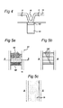
- Figures 5a, 5b, 5c show schematically a plane view of the channel region in a first, a second and a third embodiment, respectively.
- Figures 5a, 5b and 5c show a plane view of a channel region 13, below which the gate G1, depicted by dashed lines, is located (and also, if not removed by the etching process for silicon mentioned above, the gate dielectric GD, not shown here).
- a source region 5 is located, and on the other side a drain region 5 is located.
- a first embodiment is shown wherein a plurality of quantum-dots QD is arranged as channel layer 13 between source and drain.
- the quantum-dots may be ordered as an array (lower part of Figure 5a) or may be ordered in some random network (upper part of Figure 5a).
- a second embodiment is shown wherein a plurality of quantum-wires QW is arranged as channel layer 13 between source and drain regions 5.
- the quantum-wires QW are lengthwise arranged, with one end of the quantum-wire QW being in contact with the source region and the other end being in contact with the drain region.
- Figure 5c a third embodiment is shown wherein the channel layer 13 is a continuous medium between source/drain regions.
- inventions as shown in Figures 4, 5a, 5b, 5c may be further processed by suitable, known IC processing techniques for passivation, metallization and contacting to obtain a microelectronic device comprising a MOSFET structure according to one of the embodiments as described above.
- the transistor structure as described above may differ from a MOSFET; the gate region G1 may comprise Si, but may also consist of a metal.
- the gate dielectric may be a gate oxide but may also be a high-k material such as Si 3 N 4 .
- a second gate stack (not shown) may be formed in a further deposition process. Subsequently, processing techniques for passivation, metallization and contacting may be applied for creating a microelectronic device with a double gate structure.
- the structure of source, drain and channel regions 5, 13 according to the present invention may also be embodied in a bipolar transistor, wherein the gate G1 is arranged as an emitter, the channel region 13 is arranged as a collector, the gate dielectric GD is arranged as a base and the source/drain regions 5 are arranged as contacts to the base.
- the materials for emitter, collector, and base must be chosen in accordance with the bipolar transistor function of the device.
- the etching process is arranged so as to obtain smooth and abrupt interfaces between the source/drain regions 5 and the gap 12.
- the thermal budget of all successive processing steps is preferably kept to a minimum in order to keep the shape of the interfaces as abrupt as possible and to allow the formation of abrupt junctions between source/drain regions and the channel layer 13.
Landscapes
- Engineering & Computer Science (AREA)
- Physics & Mathematics (AREA)
- Nanotechnology (AREA)
- Chemical & Material Sciences (AREA)
- Microelectronics & Electronic Packaging (AREA)
- Computer Hardware Design (AREA)
- Manufacturing & Machinery (AREA)
- Power Engineering (AREA)
- Mathematical Physics (AREA)
- Theoretical Computer Science (AREA)
- General Physics & Mathematics (AREA)
- Crystallography & Structural Chemistry (AREA)
- Condensed Matter Physics & Semiconductors (AREA)
- Thin Film Transistor (AREA)
Priority Applications (1)
| Application Number | Priority Date | Filing Date | Title |
|---|---|---|---|
| EP05003842A EP1583143B1 (de) | 2004-03-29 | 2005-02-23 | Methode zur Herstellung von selbst-justierten Source/Drain-Kontakten in einem Doppel-Gate-FET unter kontrollierter Herstellung eines dünnen Si- oder Nicht-Si-Kanals |
Applications Claiming Priority (3)
| Application Number | Priority Date | Filing Date | Title |
|---|---|---|---|
| EP04101291 | 2004-03-29 | ||
| EP04101291 | 2004-03-29 | ||
| EP05003842A EP1583143B1 (de) | 2004-03-29 | 2005-02-23 | Methode zur Herstellung von selbst-justierten Source/Drain-Kontakten in einem Doppel-Gate-FET unter kontrollierter Herstellung eines dünnen Si- oder Nicht-Si-Kanals |
Publications (3)
| Publication Number | Publication Date |
|---|---|
| EP1583143A2 true EP1583143A2 (de) | 2005-10-05 |
| EP1583143A3 EP1583143A3 (de) | 2008-06-11 |
| EP1583143B1 EP1583143B1 (de) | 2011-10-05 |
Family
ID=34889026
Family Applications (1)
| Application Number | Title | Priority Date | Filing Date |
|---|---|---|---|
| EP05003842A Expired - Lifetime EP1583143B1 (de) | 2004-03-29 | 2005-02-23 | Methode zur Herstellung von selbst-justierten Source/Drain-Kontakten in einem Doppel-Gate-FET unter kontrollierter Herstellung eines dünnen Si- oder Nicht-Si-Kanals |
Country Status (1)
| Country | Link |
|---|---|
| EP (1) | EP1583143B1 (de) |
Cited By (1)
| Publication number | Priority date | Publication date | Assignee | Title |
|---|---|---|---|---|
| WO2008078133A1 (en) | 2006-12-26 | 2008-07-03 | S.O.I.Tec Silicon On Insulator Technologies | Method for producing a semiconductor-on-insulator structure |
Family Cites Families (3)
| Publication number | Priority date | Publication date | Assignee | Title |
|---|---|---|---|---|
| JP2000106441A (ja) * | 1998-09-29 | 2000-04-11 | Sony Corp | 半導体装置の製造方法 |
| US6737332B1 (en) * | 2002-03-28 | 2004-05-18 | Advanced Micro Devices, Inc. | Semiconductor device formed over a multiple thickness buried oxide layer, and methods of making same |
| JP3764401B2 (ja) * | 2002-04-18 | 2006-04-05 | 株式会社東芝 | 半導体装置の製造方法 |
-
2005
- 2005-02-23 EP EP05003842A patent/EP1583143B1/de not_active Expired - Lifetime
Cited By (2)
| Publication number | Priority date | Publication date | Assignee | Title |
|---|---|---|---|---|
| WO2008078133A1 (en) | 2006-12-26 | 2008-07-03 | S.O.I.Tec Silicon On Insulator Technologies | Method for producing a semiconductor-on-insulator structure |
| US7531430B2 (en) | 2006-12-26 | 2009-05-12 | S.O.I.Tec Silicon On Insulator Technologies | Method for producing a semiconductor-on-insulator structure |
Also Published As
| Publication number | Publication date |
|---|---|
| EP1583143A3 (de) | 2008-06-11 |
| EP1583143B1 (de) | 2011-10-05 |
Similar Documents
| Publication | Publication Date | Title |
|---|---|---|
| US11784185B2 (en) | Source/drain regions in fin field effect transistors (FinFETs) and methods of forming same | |
| US11557659B2 (en) | Gate all around transistor device and fabrication methods thereof | |
| US7105934B2 (en) | FinFET with low gate capacitance and low extrinsic resistance | |
| EP1519420A2 (de) | Halbleiterbauelement mit mehrfachem Gate und diesbezügliches Herstellungsverfahren | |
| US10263111B2 (en) | FinFET and method for manufacturing the same | |
| US8164137B2 (en) | Multiple-gate MOS transistor using Si substrate and method of manufacturing the same | |
| US7795112B2 (en) | Method of fabricating self-aligned source and drain contacts in a double gate FET with controlled manufacturing of a thin Si or non-Si channel | |
| CN103985754A (zh) | 半导体器件及其制造方法 | |
| US7416925B2 (en) | Doped structure for finfet devices | |
| US20230317566A1 (en) | Device with backside power rail and method | |
| US20210249531A1 (en) | Nanostructure Device and Method | |
| US20250344456A1 (en) | Interconnect structure for semiconductor device | |
| US12414356B2 (en) | Gate structure and method of forming same | |
| EP1583143B1 (de) | Methode zur Herstellung von selbst-justierten Source/Drain-Kontakten in einem Doppel-Gate-FET unter kontrollierter Herstellung eines dünnen Si- oder Nicht-Si-Kanals | |
| CN115763257A (zh) | 一种半导体器件及其制备方法 | |
| EP1503424A2 (de) | Halbleiterbauelement mit mehrfachem Gate und diesbezügliches Herstellungsverfahren | |
| US12349380B2 (en) | Gate all around transistor device and fabrication methods thereof | |
| US20070257322A1 (en) | Hybrid Transistor Structure and a Method for Making the Same | |
| CN221466586U (zh) | 半导体装置 | |
| KR102901196B1 (ko) | 컨택 레일을 구비한 반도체 구조물 및 그 형성 방법 | |
| US20250031436A1 (en) | Structure and formation method of semiconductor device with semiconductor nanostructures | |
| US20250344425A1 (en) | Source/Drain Structure of Semiconductor Device and Method of Forming Same | |
| WO2007054844A2 (en) | Vertical insulated gate field-effect transistor and method of manufacturing the same |
Legal Events
| Date | Code | Title | Description |
|---|---|---|---|
| PUAI | Public reference made under article 153(3) epc to a published international application that has entered the european phase |
Free format text: ORIGINAL CODE: 0009012 |
|
| AK | Designated contracting states |
Kind code of ref document: A2 Designated state(s): AT BE BG CH CY CZ DE DK EE ES FI FR GB GR HU IE IS IT LI LT LU MC NL PL PT RO SE SI SK TR |
|
| AX | Request for extension of the european patent |
Extension state: AL BA HR LV MK YU |
|
| PUAL | Search report despatched |
Free format text: ORIGINAL CODE: 0009013 |
|
| AK | Designated contracting states |
Kind code of ref document: A3 Designated state(s): AT BE BG CH CY CZ DE DK EE ES FI FR GB GR HU IE IS IT LI LT LU MC NL PL PT RO SE SI SK TR |
|
| AX | Request for extension of the european patent |
Extension state: AL BA HR LV MK YU |
|
| 17P | Request for examination filed |
Effective date: 20081201 |
|
| AKX | Designation fees paid |
Designated state(s): DE FR GB |
|
| RAP1 | Party data changed (applicant data changed or rights of an application transferred) |
Owner name: INTERUNIVERSITAIR MICROELEKTRONICA CENTRUM Owner name: NXP B.V. |
|
| RAP1 | Party data changed (applicant data changed or rights of an application transferred) |
Owner name: IMEC Owner name: NXP B.V. |
|
| 17Q | First examination report despatched |
Effective date: 20100625 |
|
| GRAP | Despatch of communication of intention to grant a patent |
Free format text: ORIGINAL CODE: EPIDOSNIGR1 |
|
| GRAS | Grant fee paid |
Free format text: ORIGINAL CODE: EPIDOSNIGR3 |
|
| GRAA | (expected) grant |
Free format text: ORIGINAL CODE: 0009210 |
|
| AK | Designated contracting states |
Kind code of ref document: B1 Designated state(s): DE FR GB |
|
| REG | Reference to a national code |
Ref country code: GB Ref legal event code: FG4D |
|
| REG | Reference to a national code |
Ref country code: DE Ref legal event code: R096 Ref document number: 602005030308 Country of ref document: DE Effective date: 20111201 |
|
| PLBE | No opposition filed within time limit |
Free format text: ORIGINAL CODE: 0009261 |
|
| STAA | Information on the status of an ep patent application or granted ep patent |
Free format text: STATUS: NO OPPOSITION FILED WITHIN TIME LIMIT |
|
| 26N | No opposition filed |
Effective date: 20120706 |
|
| REG | Reference to a national code |
Ref country code: DE Ref legal event code: R097 Ref document number: 602005030308 Country of ref document: DE Effective date: 20120706 |
|
| REG | Reference to a national code |
Ref country code: FR Ref legal event code: PLFP Year of fee payment: 12 |
|
| REG | Reference to a national code |
Ref country code: FR Ref legal event code: PLFP Year of fee payment: 13 |
|
| REG | Reference to a national code |
Ref country code: FR Ref legal event code: PLFP Year of fee payment: 14 |
|
| P01 | Opt-out of the competence of the unified patent court (upc) registered |
Effective date: 20230513 |
|
| PGFP | Annual fee paid to national office [announced via postgrant information from national office to epo] |
Ref country code: DE Payment date: 20240123 Year of fee payment: 20 Ref country code: GB Payment date: 20240123 Year of fee payment: 20 |
|
| PGFP | Annual fee paid to national office [announced via postgrant information from national office to epo] |
Ref country code: FR Payment date: 20240123 Year of fee payment: 20 |
|
| REG | Reference to a national code |
Ref country code: DE Ref legal event code: R079 Ref document number: 602005030308 Country of ref document: DE Free format text: PREVIOUS MAIN CLASS: H01L0021336000 Ipc: H10D0030010000 |
|
| REG | Reference to a national code |
Ref country code: DE Ref legal event code: R071 Ref document number: 602005030308 Country of ref document: DE |
|
| REG | Reference to a national code |
Ref country code: GB Ref legal event code: PE20 Expiry date: 20250222 |
|
| PG25 | Lapsed in a contracting state [announced via postgrant information from national office to epo] |
Ref country code: GB Free format text: LAPSE BECAUSE OF EXPIRATION OF PROTECTION Effective date: 20250222 |