EP1580903A1 - Semiconductor device - Google Patents
Semiconductor device Download PDFInfo
- Publication number
- EP1580903A1 EP1580903A1 EP03768181A EP03768181A EP1580903A1 EP 1580903 A1 EP1580903 A1 EP 1580903A1 EP 03768181 A EP03768181 A EP 03768181A EP 03768181 A EP03768181 A EP 03768181A EP 1580903 A1 EP1580903 A1 EP 1580903A1
- Authority
- EP
- European Patent Office
- Prior art keywords
- memory
- random number
- semiconductor device
- information
- plural
- Prior art date
- Legal status (The legal status is an assumption and is not a legal conclusion. Google has not performed a legal analysis and makes no representation as to the accuracy of the status listed.)
- Granted
Links
Images


Classifications
-
- G—PHYSICS
- G06—COMPUTING OR CALCULATING; COUNTING
- G06K—GRAPHICAL DATA READING; PRESENTATION OF DATA; RECORD CARRIERS; HANDLING RECORD CARRIERS
- G06K7/00—Methods or arrangements for sensing record carriers, e.g. for reading patterns
- G06K7/10—Methods or arrangements for sensing record carriers, e.g. for reading patterns by electromagnetic radiation, e.g. optical sensing; by corpuscular radiation
- G06K7/10009—Methods or arrangements for sensing record carriers, e.g. for reading patterns by electromagnetic radiation, e.g. optical sensing; by corpuscular radiation sensing by radiation using wavelengths larger than 0.1 mm, e.g. radio-waves or microwaves
- G06K7/10019—Methods or arrangements for sensing record carriers, e.g. for reading patterns by electromagnetic radiation, e.g. optical sensing; by corpuscular radiation sensing by radiation using wavelengths larger than 0.1 mm, e.g. radio-waves or microwaves resolving collision on the communication channels between simultaneously or concurrently interrogated record carriers.
- G06K7/10029—Methods or arrangements for sensing record carriers, e.g. for reading patterns by electromagnetic radiation, e.g. optical sensing; by corpuscular radiation sensing by radiation using wavelengths larger than 0.1 mm, e.g. radio-waves or microwaves resolving collision on the communication channels between simultaneously or concurrently interrogated record carriers. the collision being resolved in the time domain, e.g. using binary tree search or RFID responses allocated to a random time slot
- G06K7/10039—Methods or arrangements for sensing record carriers, e.g. for reading patterns by electromagnetic radiation, e.g. optical sensing; by corpuscular radiation sensing by radiation using wavelengths larger than 0.1 mm, e.g. radio-waves or microwaves resolving collision on the communication channels between simultaneously or concurrently interrogated record carriers. the collision being resolved in the time domain, e.g. using binary tree search or RFID responses allocated to a random time slot interrogator driven, i.e. synchronous
-
- G—PHYSICS
- G06—COMPUTING OR CALCULATING; COUNTING
- G06K—GRAPHICAL DATA READING; PRESENTATION OF DATA; RECORD CARRIERS; HANDLING RECORD CARRIERS
- G06K19/00—Record carriers for use with machines and with at least a part designed to carry digital markings
- G06K19/06—Record carriers for use with machines and with at least a part designed to carry digital markings characterised by the kind of the digital marking, e.g. shape, nature, code
- G06K19/067—Record carriers with conductive marks, printed circuits or semiconductor circuit elements, e.g. credit or identity cards also with resonating or responding marks without active components
- G06K19/07—Record carriers with conductive marks, printed circuits or semiconductor circuit elements, e.g. credit or identity cards also with resonating or responding marks without active components with integrated circuit chips
- G06K19/077—Constructional details, e.g. mounting of circuits in the carrier
-
- G—PHYSICS
- G06—COMPUTING OR CALCULATING; COUNTING
- G06K—GRAPHICAL DATA READING; PRESENTATION OF DATA; RECORD CARRIERS; HANDLING RECORD CARRIERS
- G06K19/00—Record carriers for use with machines and with at least a part designed to carry digital markings
- G06K19/06—Record carriers for use with machines and with at least a part designed to carry digital markings characterised by the kind of the digital marking, e.g. shape, nature, code
- G06K19/067—Record carriers with conductive marks, printed circuits or semiconductor circuit elements, e.g. credit or identity cards also with resonating or responding marks without active components
- G06K19/07—Record carriers with conductive marks, printed circuits or semiconductor circuit elements, e.g. credit or identity cards also with resonating or responding marks without active components with integrated circuit chips
- G06K19/0723—Record carriers with conductive marks, printed circuits or semiconductor circuit elements, e.g. credit or identity cards also with resonating or responding marks without active components with integrated circuit chips the record carrier comprising an arrangement for non-contact communication, e.g. wireless communication circuits on transponder cards, non-contact smart cards or RFIDs
-
- G—PHYSICS
- G06—COMPUTING OR CALCULATING; COUNTING
- G06K—GRAPHICAL DATA READING; PRESENTATION OF DATA; RECORD CARRIERS; HANDLING RECORD CARRIERS
- G06K7/00—Methods or arrangements for sensing record carriers, e.g. for reading patterns
- G06K7/0008—General problems related to the reading of electronic memory record carriers, independent of its reading method, e.g. power transfer
-
- H—ELECTRICITY
- H04—ELECTRIC COMMUNICATION TECHNIQUE
- H04B—TRANSMISSION
- H04B5/00—Near-field transmission systems, e.g. inductive or capacitive transmission systems
- H04B5/40—Near-field transmission systems, e.g. inductive or capacitive transmission systems characterised by components specially adapted for near-field transmission
- H04B5/48—Transceivers
Definitions
- a sixth means for solving the above-described problem exists in a semiconductor device having a memory which memorizes the first random number and information other than the first random number, the semiconductor device sending information in the memory in non-contact condition with a time difference according to a numeric value of the first random number and being characterized in that carrier signal from outside the semiconductor device is changed from L level to H level and remains in that state over a specified time and after that, drops to the L level and after a predetermined time elapses, returns to H level, recognizing that a first clock comes.
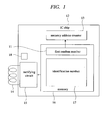
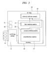
- the first flip-flop 18 When the content of the memory address counter 13 reaches a specified code (for example "0"), the first flip-flop 18 is set to "L" and information in the memory 16 such as the identification number 17 is sent to an external reception unit through the rectifying circuit 15 and the antenna 14.
- a specified code for example "0"
- the semiconductor device of the second embodiment is, for example, an IC chip 12, which is equipped with a second flip-flop 21 in addition to the semiconductor device of the first embodiment and includes a second random number 22 additionally as information in the memory 16.
- the second random number 22 is set in the memory address counter 13 and counted up or counted down.
- the function of the second flip-flop 21 will be briefly described.
- a stage for setting the second random number 22 within the memory 16 in the memory address counter 13 is temporarily necessary. This is set when the output of the second flip-flop 21 is "H".
- the output of the second flip-flop 21 is set to "L" so that information in the memory 16 such as the identification number 17 is sent out according to a memory address.
- FIG. 3 is a signal waveform diagram showing a reception signal of the semiconductor device according to the third embodiment of the present invention.
- FIG. 4 is an explanatory diagram of anti-collision control method in case where plural IC tags exist according to the fourth embodiment of the present invention.
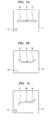
- FIGs. 5A to 5C are configuration diagrams showing the IC tag loaded with the semiconductor device (IC chip 12) of the first-third embodiments.
- the positions of the tag sheet 51, the index 54 and the IC chip 12 are common, three kinds of the IC tags each having a different antenna configuration are achieved.
- a necessity of hopping the frequency of the reception unit is generated. If antennas of the same shape overlap, two antennas come to exist in the same electric wave area so that energy of each tag decreases, thereby inducing a drop in communication distance.
- the index 54 indicates the direction of the tag sheet 51 and is used for aligning the direction of the tag sheet when the tag sheet is bonded.
- the present invention is not restricted to this, but the present invention can be applied to other semiconductor devices and particularly, theeffectofthepresent invention is more valid as the size of the semiconductor device decreases.
Landscapes
- Engineering & Computer Science (AREA)
- Physics & Mathematics (AREA)
- Theoretical Computer Science (AREA)
- General Physics & Mathematics (AREA)
- Computer Networks & Wireless Communication (AREA)
- Toxicology (AREA)
- Artificial Intelligence (AREA)
- Health & Medical Sciences (AREA)
- Computer Hardware Design (AREA)
- Microelectronics & Electronic Packaging (AREA)
- Computer Vision & Pattern Recognition (AREA)
- Electromagnetism (AREA)
- General Health & Medical Sciences (AREA)
- Signal Processing (AREA)
- Near-Field Transmission Systems (AREA)
- Storage Device Security (AREA)
- Credit Cards Or The Like (AREA)
- Radar Systems Or Details Thereof (AREA)
- Semiconductor Integrated Circuits (AREA)
Abstract
Description
Claims (5)
- A semiconductor device comprising:wherein the first random number in the memory is set in the memory address counter and information in the memory is sent out non-contact condition with a time difference according to a numeric value of the first random number.a memory which memorizes a first random number and other information; anda memory address counter indicating an address of the memory,
- A semiconductor device having a memory for memorizing a first random number and other information,
wherein the plural semiconductor devices operate synchronously with a clock from outside and when operations of the plural semiconductor devices are detected in a reception unit located outside the semiconductor devices, each of the semiconductor devices sends out information in the memory non-contact condition with a time difference according to a numeric value of the first random member. - The semiconductor device according to claim 2,
wherein the memory memorizes a second random number and when it is detected that the first random numbers of the plural semiconductor devices are identical in the reception unit, each of the semiconductor devices sends out information in the memory with a time difference according to a numeric value of the second random number. - The semiconductor device according to claim 2,
wherein the memory memorizes an error detection code and when the plural semiconductor devices operates synchronously with a clock from outside, the error detection code is sent out from the plural semiconductor devices and the reception unit receives the error detection code as a logical sum, recognizing that it is an error detection code which never appears when a single semiconductor device sends out so as to detect the operation of the plural semiconductor devices. - A semiconductor device comprising:wherein the first random number in the memory is set in the counter and the content of the counter is changed according to a clock from outside and when the content of the counter reaches a specified code, information in the memory is sent in non-contact condition.a memory which memorizes a first random number and other information; anda counter having a bit count equal to the first random number,
Priority Applications (1)
| Application Number | Priority Date | Filing Date | Title |
|---|---|---|---|
| EP06016361A EP1724710B1 (en) | 2002-12-25 | 2003-12-24 | Semiconductor device |
Applications Claiming Priority (3)
| Application Number | Priority Date | Filing Date | Title |
|---|---|---|---|
| JP2002374168A JP2004206371A (en) | 2002-12-25 | 2002-12-25 | Semiconductor device |
| JP2002374168 | 2002-12-25 | ||
| PCT/JP2003/016593 WO2004059867A1 (en) | 2002-12-25 | 2003-12-24 | Semiconductor device |
Related Child Applications (1)
| Application Number | Title | Priority Date | Filing Date |
|---|---|---|---|
| EP06016361A Division EP1724710B1 (en) | 2002-12-25 | 2003-12-24 | Semiconductor device |
Publications (3)
| Publication Number | Publication Date |
|---|---|
| EP1580903A1 true EP1580903A1 (en) | 2005-09-28 |
| EP1580903A4 EP1580903A4 (en) | 2006-06-14 |
| EP1580903B1 EP1580903B1 (en) | 2008-05-28 |
Family
ID=32677283
Family Applications (2)
| Application Number | Title | Priority Date | Filing Date |
|---|---|---|---|
| EP06016361A Expired - Lifetime EP1724710B1 (en) | 2002-12-25 | 2003-12-24 | Semiconductor device |
| EP03768181A Expired - Lifetime EP1580903B1 (en) | 2002-12-25 | 2003-12-24 | Semiconductor device |
Family Applications Before (1)
| Application Number | Title | Priority Date | Filing Date |
|---|---|---|---|
| EP06016361A Expired - Lifetime EP1724710B1 (en) | 2002-12-25 | 2003-12-24 | Semiconductor device |
Country Status (8)
| Country | Link |
|---|---|
| US (1) | US20060114103A1 (en) |
| EP (2) | EP1724710B1 (en) |
| JP (1) | JP2004206371A (en) |
| KR (2) | KR100764383B1 (en) |
| AU (1) | AU2003292765A1 (en) |
| DE (2) | DE60327115D1 (en) |
| TW (1) | TW200418169A (en) |
| WO (1) | WO2004059867A1 (en) |
Families Citing this family (6)
| Publication number | Priority date | Publication date | Assignee | Title |
|---|---|---|---|---|
| KR100935968B1 (en) | 2003-08-11 | 2010-01-08 | 가부시키가이샤 히타치세이사쿠쇼 | Reading method and answering machine and interrogator |
| US7362212B2 (en) | 2004-09-24 | 2008-04-22 | Battelle Memorial Institute | Communication methods, systems, apparatus, and devices involving RF tag registration |
| US7973644B2 (en) * | 2007-01-30 | 2011-07-05 | Round Rock Research, Llc | Systems and methods for RFID tag arbitration where RFID tags generate multiple random numbers for different arbitration sessions |
| KR100837417B1 (en) * | 2007-03-08 | 2008-06-12 | 함기형 | Permanent Wave Device |
| US8068031B2 (en) * | 2008-02-08 | 2011-11-29 | Avery Dennison Corporation | RFID devices and methods for overlapped objects |
| US10450778B2 (en) * | 2015-04-24 | 2019-10-22 | Southco, Inc. | Latch with indicator and latch system |
Family Cites Families (18)
| Publication number | Priority date | Publication date | Assignee | Title |
|---|---|---|---|---|
| US3944928A (en) * | 1974-07-01 | 1976-03-16 | Microlab/Fxr | Harmonic communication system |
| US4471345A (en) * | 1982-03-05 | 1984-09-11 | Sensormatic Electronics Corporation | Randomized tag to portal communication system |
| NL8901659A (en) * | 1989-06-30 | 1991-01-16 | Nedap Nv | MULTIPASS SYSTEM. |
| JPH05232218A (en) * | 1992-02-21 | 1993-09-07 | Olympus Optical Co Ltd | Dynamic mode investigation system |
| JPH07140236A (en) * | 1993-11-17 | 1995-06-02 | Sekisui Chem Co Ltd | Wireless response system |
| US5550547A (en) * | 1994-09-12 | 1996-08-27 | International Business Machines Corporation | Multiple item radio frequency tag identification protocol |
| JPH08181633A (en) * | 1994-12-26 | 1996-07-12 | Toshiba Corp | Information gathering system |
| GB9505810D0 (en) * | 1995-03-22 | 1995-05-10 | Int Computers Ltd | Electronic identification system |
| US5591951A (en) * | 1995-10-12 | 1997-01-07 | The Regents Of The University Of California | System and method for simultaneously collecting serial number information from numerous identity tags |
| FR2741979B1 (en) * | 1995-12-01 | 1998-01-23 | Raimbault Pierre | METHOD FOR REMOTE QUERYING STATION LABELS AND LABEL FOR IMPLEMENTING SAME |
| US6010075A (en) * | 1996-11-13 | 2000-01-04 | Hitachi, Ltd. | Moving object identification method and apparatus |
| US5986570A (en) * | 1997-09-03 | 1999-11-16 | Micron Communications, Inc. | Method for resolving signal collisions between multiple RFID transponders in a field |
| US6002344A (en) * | 1997-11-21 | 1999-12-14 | Bandy; William R. | System and method for electronic inventory |
| GB9804584D0 (en) * | 1998-03-04 | 1998-04-29 | Trolley Scan Pty Limited | Identification of objects by a reader |
| GB2335573B (en) * | 1998-03-18 | 2000-03-15 | Univ Singapore | An RF transponder identification system and protocol |
| EP1734461A2 (en) * | 1999-07-12 | 2006-12-20 | Matsushita Electric Industrial Co., Ltd. | Mobile body discrimination apparatus for rapidly acquiring respective data sets transmitted through modulation of reflected radio waves by transponders which are within a communication region of an interrogator apparatus |
| JP2002184872A (en) * | 2000-12-15 | 2002-06-28 | Hitachi Ltd | Semiconductor device having identification number, method of manufacturing the same, and electronic device |
| US6946951B2 (en) * | 2000-12-29 | 2005-09-20 | Tagsys Australia Pty Ltd. | System and method for interrogating electronic labels |
-
2002
- 2002-12-25 JP JP2002374168A patent/JP2004206371A/en not_active Withdrawn
-
2003
- 2003-12-23 TW TW092136580A patent/TW200418169A/en not_active IP Right Cessation
- 2003-12-24 EP EP06016361A patent/EP1724710B1/en not_active Expired - Lifetime
- 2003-12-24 KR KR1020057011754A patent/KR100764383B1/en not_active Expired - Fee Related
- 2003-12-24 US US10/540,268 patent/US20060114103A1/en not_active Abandoned
- 2003-12-24 KR KR1020067016592A patent/KR100983427B1/en not_active Expired - Fee Related
- 2003-12-24 EP EP03768181A patent/EP1580903B1/en not_active Expired - Lifetime
- 2003-12-24 DE DE60327115T patent/DE60327115D1/en not_active Expired - Lifetime
- 2003-12-24 AU AU2003292765A patent/AU2003292765A1/en not_active Abandoned
- 2003-12-24 DE DE60321387T patent/DE60321387D1/en not_active Expired - Lifetime
- 2003-12-24 WO PCT/JP2003/016593 patent/WO2004059867A1/en not_active Ceased
Also Published As
| Publication number | Publication date |
|---|---|
| TWI336518B (en) | 2011-01-21 |
| EP1580903A4 (en) | 2006-06-14 |
| TW200418169A (en) | 2004-09-16 |
| KR100764383B1 (en) | 2007-10-08 |
| WO2004059867A1 (en) | 2004-07-15 |
| EP1724710A2 (en) | 2006-11-22 |
| AU2003292765A1 (en) | 2004-07-22 |
| DE60321387D1 (en) | 2008-07-10 |
| EP1580903B1 (en) | 2008-05-28 |
| EP1724710A3 (en) | 2007-01-10 |
| DE60327115D1 (en) | 2009-05-20 |
| US20060114103A1 (en) | 2006-06-01 |
| JP2004206371A (en) | 2004-07-22 |
| KR100983427B1 (en) | 2010-09-20 |
| KR20060107583A (en) | 2006-10-13 |
| KR20050089162A (en) | 2005-09-07 |
| EP1724710B1 (en) | 2009-04-08 |
Similar Documents
| Publication | Publication Date | Title |
|---|---|---|
| KR101048612B1 (en) | RFID tag recognition method to prevent RFID tag collision, RFID reader and RFID tag using same | |
| US7893815B2 (en) | Method for selecting one or several transponders | |
| EP1977375A1 (en) | Method of preventing collisions between rfid readers in rfid system | |
| EP2958056B1 (en) | Radiofrequency transponder circuit | |
| US7403122B1 (en) | RFID tag circuits operable at different speeds | |
| KR20020017846A (en) | Radio frequency identification tag system for preventing collision and collision preventing method thereof | |
| US20070237087A1 (en) | Communication medium, communication medium processing apparatus, and communication medium processing system | |
| CN101944171A (en) | Multi-tag identification method of RFID reader | |
| KR20070042441A (en) | Processing method of RDF tag, RDF reader / writer, RFP system and RDF system | |
| EP1675034A1 (en) | Contact-type data communication apparatus, transmission and reception apparatus, and transmission and reception method | |
| US8963690B2 (en) | Identification system | |
| EP1580903A1 (en) | Semiconductor device | |
| US20070069865A1 (en) | IC tag, IC tag system, and data communicating method for the IC tag | |
| CN102750501B (en) | Method for handling collision in an identification system | |
| JP4279841B2 (en) | IC tag, receiving apparatus and reading method | |
| US11120232B2 (en) | Early collision detection and handling in CDMA-based RFID systems | |
| KR100662050B1 (en) | Anti-collision method in radio wave identification device | |
| KR100831533B1 (en) | Data transfer device and method of transmitting data | |
| JP2010109782A (en) | Communications device, communicating mobile terminal, and reader/writer for non-contact ic card | |
| JP2004199450A (en) | Non-contact reader / writer | |
| US20040158782A1 (en) | Method for protected transmission of data via an air interface | |
| HK1187135B (en) | Rfid protocols with non-interacting variants | |
| HK1187135A (en) | Rfid protocols with non-interacting variants |
Legal Events
| Date | Code | Title | Description |
|---|---|---|---|
| PUAI | Public reference made under article 153(3) epc to a published international application that has entered the european phase |
Free format text: ORIGINAL CODE: 0009012 |
|
| 17P | Request for examination filed |
Effective date: 20050722 |
|
| AK | Designated contracting states |
Kind code of ref document: A1 Designated state(s): AT BE BG CH CY CZ DE DK EE ES FI FR GB GR HU IE IT LI LU MC NL PT RO SE SI SK TR |
|
| AX | Request for extension of the european patent |
Extension state: AL LT LV MK |
|
| DAX | Request for extension of the european patent (deleted) | ||
| RBV | Designated contracting states (corrected) |
Designated state(s): DE FR GB IT |
|
| A4 | Supplementary search report drawn up and despatched |
Effective date: 20060515 |
|
| RIC1 | Information provided on ipc code assigned before grant |
Ipc: G06K 7/00 20060101AFI20060509BHEP Ipc: G06K 19/07 20060101ALN20060509BHEP |
|
| 17Q | First examination report despatched |
Effective date: 20060831 |
|
| GRAP | Despatch of communication of intention to grant a patent |
Free format text: ORIGINAL CODE: EPIDOSNIGR1 |
|
| RIC1 | Information provided on ipc code assigned before grant |
Ipc: G06K 19/07 20060101ALI20070725BHEP Ipc: G06K 7/00 20060101AFI20070725BHEP |
|
| GRAS | Grant fee paid |
Free format text: ORIGINAL CODE: EPIDOSNIGR3 |
|
| GRAA | (expected) grant |
Free format text: ORIGINAL CODE: 0009210 |
|
| AK | Designated contracting states |
Kind code of ref document: B1 Designated state(s): DE FR GB IT |
|
| REG | Reference to a national code |
Ref country code: GB Ref legal event code: FG4D |
|
| REF | Corresponds to: |
Ref document number: 60321387 Country of ref document: DE Date of ref document: 20080710 Kind code of ref document: P |
|
| PLBE | No opposition filed within time limit |
Free format text: ORIGINAL CODE: 0009261 |
|
| STAA | Information on the status of an ep patent application or granted ep patent |
Free format text: STATUS: NO OPPOSITION FILED WITHIN TIME LIMIT |
|
| 26N | No opposition filed |
Effective date: 20090303 |
|
| PGFP | Annual fee paid to national office [announced via postgrant information from national office to epo] |
Ref country code: DE Payment date: 20141216 Year of fee payment: 12 Ref country code: GB Payment date: 20141224 Year of fee payment: 12 |
|
| PGFP | Annual fee paid to national office [announced via postgrant information from national office to epo] |
Ref country code: FR Payment date: 20141208 Year of fee payment: 12 |
|
| PGFP | Annual fee paid to national office [announced via postgrant information from national office to epo] |
Ref country code: IT Payment date: 20141126 Year of fee payment: 12 |
|
| REG | Reference to a national code |
Ref country code: DE Ref legal event code: R119 Ref document number: 60321387 Country of ref document: DE |
|
| GBPC | Gb: european patent ceased through non-payment of renewal fee |
Effective date: 20151224 |
|
| REG | Reference to a national code |
Ref country code: FR Ref legal event code: ST Effective date: 20160831 |
|
| PG25 | Lapsed in a contracting state [announced via postgrant information from national office to epo] |
Ref country code: GB Free format text: LAPSE BECAUSE OF NON-PAYMENT OF DUE FEES Effective date: 20151224 Ref country code: DE Free format text: LAPSE BECAUSE OF NON-PAYMENT OF DUE FEES Effective date: 20160701 |
|
| PG25 | Lapsed in a contracting state [announced via postgrant information from national office to epo] |
Ref country code: FR Free format text: LAPSE BECAUSE OF NON-PAYMENT OF DUE FEES Effective date: 20151231 |
|
| PG25 | Lapsed in a contracting state [announced via postgrant information from national office to epo] |
Ref country code: IT Free format text: LAPSE BECAUSE OF NON-PAYMENT OF DUE FEES Effective date: 20151224 |