EP1580874A2 - Method and apparatus for robust mode selection with low power consumption - Google Patents
Method and apparatus for robust mode selection with low power consumption Download PDFInfo
- Publication number
- EP1580874A2 EP1580874A2 EP04257752A EP04257752A EP1580874A2 EP 1580874 A2 EP1580874 A2 EP 1580874A2 EP 04257752 A EP04257752 A EP 04257752A EP 04257752 A EP04257752 A EP 04257752A EP 1580874 A2 EP1580874 A2 EP 1580874A2
- Authority
- EP
- European Patent Office
- Prior art keywords
- voltage
- terminal
- circuit
- current
- selector terminal
- Prior art date
- Legal status (The legal status is an assumption and is not a legal conclusion. Google has not performed a legal analysis and makes no representation as to the accuracy of the status listed.)
- Withdrawn
Links
- 238000000034 method Methods 0.000 title abstract description 16
- 230000004044 response Effects 0.000 claims abstract description 10
- 230000036039 immunity Effects 0.000 description 8
- 230000001105 regulatory effect Effects 0.000 description 4
- 230000008859 change Effects 0.000 description 2
- 238000010586 diagram Methods 0.000 description 2
- 239000003990 capacitor Substances 0.000 description 1
- 238000012986 modification Methods 0.000 description 1
- 230000004048 modification Effects 0.000 description 1
- 230000000737 periodic effect Effects 0.000 description 1
- 239000004065 semiconductor Substances 0.000 description 1
- 230000035945 sensitivity Effects 0.000 description 1
Images


Classifications
-
- H—ELECTRICITY
- H02—GENERATION; CONVERSION OR DISTRIBUTION OF ELECTRIC POWER
- H02M—APPARATUS FOR CONVERSION BETWEEN AC AND AC, BETWEEN AC AND DC, OR BETWEEN DC AND DC, AND FOR USE WITH MAINS OR SIMILAR POWER SUPPLY SYSTEMS; CONVERSION OF DC OR AC INPUT POWER INTO SURGE OUTPUT POWER; CONTROL OR REGULATION THEREOF
- H02M1/00—Details of apparatus for conversion
- H02M1/32—Means for protecting converters other than automatic disconnection
-
- H—ELECTRICITY
- H02—GENERATION; CONVERSION OR DISTRIBUTION OF ELECTRIC POWER
- H02M—APPARATUS FOR CONVERSION BETWEEN AC AND AC, BETWEEN AC AND DC, OR BETWEEN DC AND DC, AND FOR USE WITH MAINS OR SIMILAR POWER SUPPLY SYSTEMS; CONVERSION OF DC OR AC INPUT POWER INTO SURGE OUTPUT POWER; CONTROL OR REGULATION THEREOF
- H02M3/00—Conversion of DC power input into DC power output
- H02M3/02—Conversion of DC power input into DC power output without intermediate conversion into AC
- H02M3/04—Conversion of DC power input into DC power output without intermediate conversion into AC by static converters
- H02M3/10—Conversion of DC power input into DC power output without intermediate conversion into AC by static converters using discharge tubes with control electrode or semiconductor devices with control electrode
- H02M3/145—Conversion of DC power input into DC power output without intermediate conversion into AC by static converters using discharge tubes with control electrode or semiconductor devices with control electrode using devices of a triode or transistor type requiring continuous application of a control signal
- H02M3/155—Conversion of DC power input into DC power output without intermediate conversion into AC by static converters using discharge tubes with control electrode or semiconductor devices with control electrode using devices of a triode or transistor type requiring continuous application of a control signal using semiconductor devices only
- H02M3/156—Conversion of DC power input into DC power output without intermediate conversion into AC by static converters using discharge tubes with control electrode or semiconductor devices with control electrode using devices of a triode or transistor type requiring continuous application of a control signal using semiconductor devices only with automatic control of output voltage or current, e.g. switching regulators
- H02M3/158—Conversion of DC power input into DC power output without intermediate conversion into AC by static converters using discharge tubes with control electrode or semiconductor devices with control electrode using devices of a triode or transistor type requiring continuous application of a control signal using semiconductor devices only with automatic control of output voltage or current, e.g. switching regulators including plural semiconductor devices as final control devices for a single load
Definitions
- the present invention relates generally to integrated circuits, and more specifically, the present invention relates to integrated circuits that are controllers for switching power supplies.
- integrated circuits for switching power supplies should have options that allow them to be used in a variety of different applications.
- the integrated circuits should require as few discrete components as possible, and they should consume the lowest possible power in operation.
- An example of a desirable option is the ability to select different switching frequencies so that an optimal design can be achieved for different applications of a single integrated circuit.
- the package of the integrated circuit should also have as few terminals as possible to minimize cost.
- a circuit comprising:
- An embodiment of a method to select multiple optional modes of operation of an integrated circuit uses a voltage between a mode selector terminal and a ground reference terminal to select operational modes. It allows one mode of operation corresponding to no connection at the terminal. The method allows the operational mode corresponding to no connection at the terminal to be robust in the presence of noise while reducing the power to maintain the desired selection in all modes of operation.
- an operational mode of a circuit is selected when the selector terminal has no external connection and also when it is connected to a source of regulated voltage that can be another terminal on the integrated circuit.
- the selector terminal When the selector terminal is not connected to a source of regulated voltage, the voltage on the selector terminal is maintained within boundaries in the presence of noise by switched current sources that absorb noise currents at the selector terminal.
- the current sources change in magnitude according to the voltage on the selector terminal. The magnitudes of the current sources are greatly reduced when the selector terminal is connected to an external voltage that is outside the voltage boundaries for the unconnected selector terminal to reduce the power consumed by the integrated circuit.
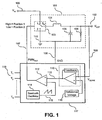
- FIG. 1 is a diagram of an example switching power supply with an integrated circuit controller that could employ an embodiment of the present invention.
- An unregulated DC input voltage V IN 100 is converted to a regulated DC output voltage V OUT 102 by switching converter 101 that is controlled by integrated circuit 117. All voltages are with respect to the ground (earth) reference 111.
- the state of a single pole double throw power switch S P 103 is controlled by the signal PWM OUT 107 from the integrated circuit 117.
- Switch S P 103 couples the inductor 104 to the input voltage V IN 100 when PWM OUT on line 107 is high.
- Switch S P 103 couples one end of the inductor 104 to the ground reference 111 when the signal PWM OUT on line 107 is low.
- Capacitor 105 filters the AC current in inductor 104 to provide a substantially DC voltage to the load 106.
- the frequency of the sawtooth oscillator 114 within integrated circuit controller 117 determines the rate of switching.
- a plurality of functional terminals 118 on the integrated circuit 117 can be coupled to operate the various functions of integrated circuit 117 in a desired manner.
- functional terminals 118 might set the frequency of the oscillator 114.
- the frequency could take on any number of values depending on the number of terminals used to implement the selection and the stimulus required at functional terminals 118.
- a stimulus could take the form of a voltage, a current, or the equivalent that could be determined by a discrete component connected between two terminals.
- a single terminal could select multiple options by connection to multiple levels of voltage or current. In any case, it is desired in one embodiment that the method of selection does not require the use of discrete components, and that the selected options maintain the lowest possible power consumption of the integrated circuit.
- Integrated circuit 117 senses the output voltage V OUT 102 of the switching converter 101 at a terminal V SENSE 109 with respect to a ground terminal GND 108.
- an error amplifier 110 within the integrated circuit 117 amplifies the difference between the voltage at terminal V SENSE 109 and a reference voltage 116 internal to the integrated circuit 117.
- a comparator 112 compares the error voltage output 113 of error amplifier 110 to the sawtooth voltage V F 115 that is an output of the oscillator 114.
- the output 107 of the comparator 112 is high when the error voltage 113 is greater than sawtooth voltage 115.
- the output 107 of comparator 112 is low when the error voltage 113 is less than the sawtooth voltage 115.
- the periodic switching of power switch S P 103 is modulated by the integrated circuit 117 in a manner to regulate the output voltage V OUT 102.
- semiconductor devices such as for example two transistors, or a transistor and a diode.
- the combination of switching converter 101 and integrated circuit controller 117 in Figure 1 is just one example of many different circuits that could be used in switching power supplies.
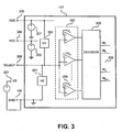
- Figure 2 illustrates one principle of voltage comparison that can be used in the design of integrated circuit controllers to select among different optional modes of operation, shown in the context of power supply controller 117. All voltages are measured with respect to the ground reference terminal 108.
- a mode select terminal 206 is coupled to a plurality of voltage comparators 202 that compare the voltage at 206 to the threshold voltages 208.
- the comparators 202 are coupled to a decoder circuit 203 that produces an output 209 to indicate which mode of operation has been selected by the voltage at the mode select terminal 206.
- a plurality of N voltage comparators 202 can determine N+1 distinct modes of operation. Each comparator determines if the voltage at the mode select terminal 206 is higher or lower than one of the threshold voltages 208. With this arrangement, N threshold voltages create N+1 possible selections. Decoder 203 enables the mode of operation that corresponds to the voltage at mode select terminal 206.
- the user sets the voltage on the mode select terminal 206 at the value appropriate for the desired optional mode of operation.
- One appropriate value could be zero, corresponding to a connection of the mode select terminal 206 to the ground reference terminal 108.
- Other appropriate values could be from internally generated voltages that are available at other functional terminals of the integrated circuit, such as voltage VDD at terminal 200 from internal voltage source 201, and VCC at terminal 204 from internal voltage source 205 in this illustration.
- voltage VDD at terminal 200 may be referred to as a first voltage bus and the ground reference terminal 108 may be referred to as a second voltage bus.
- An appropriate voltage could also be obtained from an external circuit as represented by voltage VX at node 207 in Figure 2.
- All the voltages may be obtained by direct connection of the mode select terminal 206 to a node in the power supply or to a terminal of the circuit. No discrete components are required to select an optional mode of operation. To obtain the maximum number of optional modes that may be selected with the mode select terminal 206, the unconnected or open circuit state of terminal 206 should also correspond to a predetermined mode of operation. Therefore, when mode select terminal 206 has no external connection, its voltage must be bounded between thresholds of the comparators 202.
- the arrangement in Figure 2 cannot meet the requirement for no external connection on the mode select terminal 206 because the voltage at 206 is undetermined when 206 has no external connection.
- the unconnected mode select terminal 206 is a high impedance node, whose voltage is strongly influenced by noise currents. Switching power supplies have electric and magnetic fields that can inject noise currents at the mode select terminal 206. Small noise currents with the high impedance at the mode select terminal 206 will produce voltages that cause the unintended selection of modes.
- Figure 3 shows additional internal circuits 300 and 301 that may be used to determine the voltage at 206 when select terminal 206 has no external connection.
- the internal circuits 300 and 301 also allow the selection of optional modes with mode selection terminal 206 while limiting power consumption of the integrated circuit 117. Furthermore, the circuits 300 and 301 must maintain the voltage on the mode select terminal 206 between boundaries in the presence of noise when there is no external connection to the mode select terminal 206.
- One technique to sense multiple states through a terminal of an integrated circuit requires the circuit to sense the current at the terminal, and to determine if the current is sourced to the terminal or sinked from the terminal. This technique, however, fails to reduce the power consumption of circuitry that is coupled to the terminal.
- Figure 4 shows an embodiment of circuits 300 and 301 including additional circuitry that senses the voltage directly on the mode select terminal 206.
- the embodiment illustrated in Figure 4 does not require sensing of current into or out of the mode select terminal 206. Accordingly, the embodiment illustrated in Figure 4 provides robust limits on the voltage at the mode select terminal 206 when terminal 206 has no external connection, but lacks the desired property of reduced power consumption.
- circuits 300 and 301 are current limiting circuits that are engaged by transistor switches 401 and 402 respectively.
- a switch may be defined as a device that controls the passage of electric current.
- a switch can allow any magnitude of current from zero current to the maximum current available to it, depending on its stimulus.
- transistors 401 and 402 have their respective gates held at respective voltages V G1 414 and V G2 413 by respective internal voltage sources 408 and 409. In one embodiment, V G1 is less than or equal to V G2 .
- Transistors 401 and 402 do not conduct as long as the voltage on terminal 206 is between a lower voltage boundary and an upper voltage boundary.
- the lower voltage boundary is V G1 minus the gate threshold voltage of transistor 401 while the upper voltage boundary is V G2 plus the gate threshold voltage of transistor 402.
- Noise currents that move the voltage on 206 to either the upper voltage boundary or the lower voltage boundary will cause either 401 or 402 to conduct.
- the current in transistor 401 is limited to I 1 by a current limit circuit that is current source 400.
- the current in transistor 402 is limited to 12 by a current limiting circuit that is current source 403.
- the voltage on terminal 206 will not go higher than the upper voltage boundary or lower than the lower voltage boundary as long as the noise current does not exceed respective current limits I 2 of current source 403 or I 1 of current source 400.
- the open circuit condition is robust because the voltage on the mode select terminal 206 has to go substantially higher than the upper voltage boundary or substantially lower than the lower voltage boundary to select a different mode of operation.
- transistors 404 and 407 conduct when the voltage on the mode select terminal 206 is between the lower voltage boundary and the upper voltage boundary.
- the operational mode corresponding to an open circuit on terminal 206 is set by the conduction of both transistors 404 and 407.
- transistors 404 and 407 behave like voltage comparators.
- the reference voltage for the comparator comprised of transistor 404 is VDD minus the gate threshold voltage of transistor 404.
- the reference voltage for the comparator comprised of transistor 407 is the ground reference 108 plus the gate threshold of transistor 407. To select a different mode of operation, the voltage on the mode select terminal 206 must go higher than VDD minus the gate threshold voltage of transistor 404 or lower than the ground reference plus the gate threshold voltage of transistor 407.
- Noise current can cause the voltage on the mode select terminal 206 to go high enough or low enough to change the mode of operation only if the noise current entering terminal 206 is greater than current limit I 2 of current source 403 or if the noise current leaving terminal 206 is greater than current limit I 1 of current source 400.
- High immunity to noise is achieved by making I 1 and I 2 large.
- current source 400 has the single constant value I 1 and current source 403 has the single constant value I 2 .
- I 1 and I 2 A disadvantage with making I 1 and I 2 large is that the mode select terminal 206 will conduct the large current I 1 or I 2 when the other modes of operation are selected. Large current requires proportionally large power from the internal or external voltage source that provides the current, and the circuit that receives the current consumes the power. It is desirable to consume as little power as possible and at the same time provide high immunity to noise.
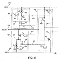
- Figure 5 shows one embodiment of a circuit that solves the problem of large power consumption while maintaining high immunity to noise on the mode select terminal 206.
- the circuit of Figure 5 may be a selector circuit, which may be included in an integrated circuit device.
- the integrated circuit device may be a controller of a switching power supply, such as for example one similar to that illustrated in Figure 1.
- circuit 300 is coupled between selector terminal 206 and a first voltage bus, shown in the depicted embodiment as VDD 200.
- circuit 301 is coupled between selector terminal 206 and ground reference terminal 108. It is appreciated that VDD 200 and ground terminal 108 may be considered as first and second voltage busses.
- circuit 300 is adapted to vary a current limit out of selector terminal 206 in response to the voltage at selector terminal 206 and circuit 301 is adapted to vary a current limit into selector terminal 206 in response to the voltage at selector terminal 206.
- the circuit also includes a plurality of voltage comparators 202 coupled to selector terminal 206 and coupled to circuits 300 and 301.
- the plurality of voltage comparators are also coupled to a decoder circuit such as for example decoder circuit 203.
- circuit 300 includes a variable current source 400 and that circuit 301 includes a variable current source 403.
- the current limiting circuit 400 in Figure 4 is fixed at a single value I 1
- the current limiting circuit 400 in Figure 5 is a variable current limit circuit with at least two possible values: a high value and a low value.
- the current limiting circuit 403 in Figure 4 is fixed at a single value I 2
- the current limiting circuit 403 in Figure 5 is also a variable current limit circuit with at least two possible values: a high value and a low value.
- the high value is engaged to obtain high immunity to noise when the voltage on the mode select terminal 206 has no external connection.
- the low value is engaged when the mode select terminal 206 is connected to a hard voltage source that does not require the high current for immunity to noise.
- the low value needs to be only large enough to return the voltage on the mode select terminal 206 to between the two boundaries that are defined by V G1 , V G2 , and the respective gate threshold voltages of transistors 401 and 402 when the mode select terminal is disconnected from the hard voltage source.
- the variable current limiting circuit 400 includes two fixed current sources.
- One fixed current source is current source 501, which has a magnitude I L1 .
- the other fixed current source is current source 500, which has a magnitude I H1 .
- the magnitude of current source 501 is substantially less than the magnitude of current source 500.
- Transistor switch 502 determines whether or not the high magnitude current source 500 adds to the low magnitude current source 501.
- variable current limiting circuit 403 in Figure 5 includes two fixed current sources.
- One fixed current source is current source 503, which has a magnitude I L2 .
- the other fixed current source is current source 504, which has a magnitude I H2 .
- the magnitude of current source 503 is substantially less than the magnitude of current source 504.
- Transistor switch 505 determines whether or not the high magnitude current source 504 adds to the low magnitude current source 503.
- variable current limiting circuit 400 in Figure 5 switches from a high current to a low current when the voltage on the mode select terminal 206 is less than a gate threshold voltage of transistor 407 above the ground reference. This voltage near the ground reference on the mode select terminal 206 selects a different mode of operation.
- the switching between high and low values is accomplished by transistor 502 that is coupled to the output 412 of a voltage comparator comprised of transistor 407.
- the high current limit that gives immunity to noise is not required under this condition because in practice the voltage on the mode select terminal 206 will be fixed by an external connection to a hard voltage such as for example the ground reference terminal 108.
- variable current limiting circuit 403 in the embodiment of Figure 5 switches from a high current to a low current when the voltage on the mode select terminal 206 is greater than the voltage VDD at terminal 200 minus the gate threshold voltage of transistor 404.
- This voltage near VDD on the mode select terminal 206 selects a different mode of operation.
- the switching of the current source between high and low values is accomplished by transistor 505 that is coupled to the output 411 of a voltage comparator comprised of transistor 404.
- the high current that gives noise immunity is not required under this condition because in practice the voltage on mode select terminal 206 will be fixed by an external connection to a regulated voltage such as for example VDD terminal 200.
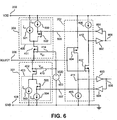
- FIG. 6 is a schematic illustrating another embodiment of the present invention in which inverters 601, 602, 603 and 604 are added to the embodiment of Figure 5.
- inverters 601, 602, 603 and 604 help assure that the signals at the lines 506, 606, 605 and 507 respectively have sufficient drive for reliable operation.
- the gate 414 of transistor 401 and the gate 413 of transistor 402 are coupled to a reference voltage 600, which in one embodiment is half the power supply voltage VDD 200.
- the value of half the power supply voltage VDD for the reference voltage 600 in the embodiment of Figure 6 gives the greatest immunity to noise when the mode select terminal 206 has no external connection.
Landscapes
- Engineering & Computer Science (AREA)
- Power Engineering (AREA)
- Dc-Dc Converters (AREA)
- Semiconductor Integrated Circuits (AREA)
- Logic Circuits (AREA)
Abstract
Description
- The present invention relates generally to integrated circuits, and more specifically, the present invention relates to integrated circuits that are controllers for switching power supplies.
- It is well known that the use of integrated circuits to replace discrete components in electronic circuits can reduce the cost and size of electronic systems. The use of integrated circuits also reduces the power required to operate those systems. A category of electronic systems that benefits from the use of integrated circuits is electronic power supplies. The parameters of cost, size, and power consumption are especially important in application of these systems. Switching power supplies are of particular interest to designers of electronic systems because the highest performance is generally achieved with switching power supply technology.
- To realize the goals of systems designers, integrated circuits for switching power supplies should have options that allow them to be used in a variety of different applications. The integrated circuits should require as few discrete components as possible, and they should consume the lowest possible power in operation. An example of a desirable option is the ability to select different switching frequencies so that an optimal design can be achieved for different applications of a single integrated circuit. The package of the integrated circuit should also have as few terminals as possible to minimize cost.
- Accordingly, according to the invention there is provided a circuit comprising:
- a first current limiting circuit coupled between a selector terminal and a first voltage bus, the first current limiting circuit adapted to vary a current limit out of the selector terminal in response to a voltage on the selector terminal; and
- a second current limiting circuit coupled between the selector terminal and a second voltage bus, the second current limiting circuit adapted to vary a current limit into the selector terminal in response to the voltage on the selector terminal. Thus, disclosed are methods and apparatuses that allow a selector terminal of a circuit to select optional modes of operation while maintaining low power consumption with reduced sensitivity to noise. In one embodiment, a circuit according to the teachings of the present invention includes a first current limiting circuit coupled between the selector terminal and a first voltage bus. The first current limiting circuit is adapted to vary a current limit out of the selector terminal in response to a voltage on the selector terminal. The circuit also includes a second current limiting circuit coupled between the selector terminal and a second voltage bus. The second current limiting circuit adapted to vary a current limit into the selector terminal in response to the voltage on the selector terminal.
- Figure 1 shows an example of a switching power supply that includes a switching converter and an integrated circuit controller ;
- Figure 2 is a diagram illustrating the principles of a technique that uses the voltage on a terminal of an integrated circuit to select among optional modes of operation ;
- Figure 3 shows the elements added to the technique illustrated in Figure 2 to select optional modes of operation ;
- Figure 4 is a schematic illustration of functional blocks in Figure 3;
- Figure 5 is a schematic of one embodiment of a method and apparatus to select optional modes of operation in accordance with the teachings of the present invention ; and
- Figure 6 is a schematic of another embodiment of the method and apparatus to achieve the selection of optional modes of operation in accordance with the teachings of the present invention.
-
- An embodiment of a method to select multiple optional modes of operation of an integrated circuit is disclosed. The method uses a voltage between a mode selector terminal and a ground reference terminal to select operational modes. It allows one mode of operation corresponding to no connection at the terminal. The method allows the operational mode corresponding to no connection at the terminal to be robust in the presence of noise while reducing the power to maintain the desired selection in all modes of operation.
- In the following description, numerous specific details are set forth in order to provide a thorough understanding of the present invention. It will be apparent, however, to one having ordinary skill in the art that the specific detail need not be employed to practice the present invention. Well-known methods related to the implementation have not been described in detail in order to avoid obscuring the present invention.
- Reference throughout this specification to "one embodiment" or "an embodiment" means that a particular feature, structure, or characteristic described in connection with the embodiment is included in at least one embodiment of the present invention. Thus, the appearances of the phrases "in one embodiment" or "in an embodiment" in various places throughout this specification are not necessarily all referring to the same embodiment. Furthermore, the particular features, structures, or characteristics may be combined in any suitable manner in one or more embodiments.
- As will be disclosed in this disclosure, an operational mode of a circuit according to the teachings of the present invention is selected when the selector terminal has no external connection and also when it is connected to a source of regulated voltage that can be another terminal on the integrated circuit. When the selector terminal is not connected to a source of regulated voltage, the voltage on the selector terminal is maintained within boundaries in the presence of noise by switched current sources that absorb noise currents at the selector terminal. The current sources change in magnitude according to the voltage on the selector terminal. The magnitudes of the current sources are greatly reduced when the selector terminal is connected to an external voltage that is outside the voltage boundaries for the unconnected selector terminal to reduce the power consumed by the integrated circuit.
- Figure 1 is a diagram of an example switching power supply with an integrated circuit controller that could employ an embodiment of the present invention. An unregulated DC
input voltage V IN 100 is converted to a regulated DCoutput voltage V OUT 102 byswitching converter 101 that is controlled byintegrated circuit 117. All voltages are with respect to the ground (earth)reference 111. The state of a single pole double throwpower switch S P 103 is controlled by thesignal PWM OUT 107 from the integratedcircuit 117. SwitchS P 103 couples theinductor 104 to theinput voltage V IN 100 when PWMOUT online 107 is high. SwitchS P 103 couples one end of theinductor 104 to theground reference 111 when the signal PWMOUT online 107 is low.Capacitor 105 filters the AC current ininductor 104 to provide a substantially DC voltage to theload 106. The frequency of thesawtooth oscillator 114 withinintegrated circuit controller 117 determines the rate of switching. - A plurality of
functional terminals 118 on theintegrated circuit 117 can be coupled to operate the various functions ofintegrated circuit 117 in a desired manner. For example,functional terminals 118 might set the frequency of theoscillator 114. The frequency could take on any number of values depending on the number of terminals used to implement the selection and the stimulus required atfunctional terminals 118. A stimulus could take the form of a voltage, a current, or the equivalent that could be determined by a discrete component connected between two terminals. A single terminal could select multiple options by connection to multiple levels of voltage or current. In any case, it is desired in one embodiment that the method of selection does not require the use of discrete components, and that the selected options maintain the lowest possible power consumption of the integrated circuit. -
Integrated circuit 117 senses theoutput voltage V OUT 102 of theswitching converter 101 at aterminal V SENSE 109 with respect to aground terminal GND 108. In one embodiment, anerror amplifier 110 within theintegrated circuit 117 amplifies the difference between the voltage atterminal V SENSE 109 and areference voltage 116 internal to theintegrated circuit 117. Acomparator 112 compares theerror voltage output 113 oferror amplifier 110 to thesawtooth voltage V F 115 that is an output of theoscillator 114. Theoutput 107 of thecomparator 112 is high when theerror voltage 113 is greater thansawtooth voltage 115. Theoutput 107 ofcomparator 112 is low when theerror voltage 113 is less than thesawtooth voltage 115. Thus, the periodic switching ofpower switch S P 103 is modulated by the integratedcircuit 117 in a manner to regulate theoutput voltage V OUT 102. There are many ways to implement the function of theswitch S P 103 with semiconductor devices, such as for example two transistors, or a transistor and a diode. The combination ofswitching converter 101 andintegrated circuit controller 117 in Figure 1 is just one example of many different circuits that could be used in switching power supplies. - Figure 2 illustrates one principle of voltage comparison that can be used in the design of integrated circuit controllers to select among different optional modes of operation, shown in the context of
power supply controller 117. All voltages are measured with respect to theground reference terminal 108. A modeselect terminal 206 is coupled to a plurality ofvoltage comparators 202 that compare the voltage at 206 to thethreshold voltages 208. Thecomparators 202 are coupled to adecoder circuit 203 that produces anoutput 209 to indicate which mode of operation has been selected by the voltage at the modeselect terminal 206. - In the arrangement illustrated in Figure 2, a plurality of
N voltage comparators 202 can determine N+1 distinct modes of operation. Each comparator determines if the voltage at the modeselect terminal 206 is higher or lower than one of thethreshold voltages 208. With this arrangement, N threshold voltages create N+1 possible selections.Decoder 203 enables the mode of operation that corresponds to the voltage at modeselect terminal 206. - The user sets the voltage on the mode
select terminal 206 at the value appropriate for the desired optional mode of operation. One appropriate value could be zero, corresponding to a connection of the modeselect terminal 206 to theground reference terminal 108. Other appropriate values could be from internally generated voltages that are available at other functional terminals of the integrated circuit, such as voltage VDD at terminal 200 frominternal voltage source 201, and VCC at terminal 204 frominternal voltage source 205 in this illustration. For purposes of this disclosure, it is noted that voltage VDD atterminal 200 may be referred to as a first voltage bus and theground reference terminal 108 may be referred to as a second voltage bus. An appropriate voltage could also be obtained from an external circuit as represented by voltage VX atnode 207 in Figure 2. - All the voltages may be obtained by direct connection of the mode
select terminal 206 to a node in the power supply or to a terminal of the circuit. No discrete components are required to select an optional mode of operation. To obtain the maximum number of optional modes that may be selected with the modeselect terminal 206, the unconnected or open circuit state ofterminal 206 should also correspond to a predetermined mode of operation. Therefore, when modeselect terminal 206 has no external connection, its voltage must be bounded between thresholds of thecomparators 202. - It is appreciated that the arrangement in Figure 2 cannot meet the requirement for no external connection on the mode
select terminal 206 because the voltage at 206 is undetermined when 206 has no external connection. Moreover, the unconnected modeselect terminal 206 is a high impedance node, whose voltage is strongly influenced by noise currents. Switching power supplies have electric and magnetic fields that can inject noise currents at the modeselect terminal 206. Small noise currents with the high impedance at the modeselect terminal 206 will produce voltages that cause the unintended selection of modes. - Figure 3 shows additional
internal circuits select terminal 206 has no external connection. Theinternal circuits mode selection terminal 206 while limiting power consumption of theintegrated circuit 117. Furthermore, thecircuits select terminal 206 between boundaries in the presence of noise when there is no external connection to the modeselect terminal 206. - One technique to sense multiple states through a terminal of an integrated circuit, including a state corresponding to no connection at the terminal, requires the circuit to sense the current at the terminal, and to determine if the current is sourced to the terminal or sinked from the terminal. This technique, however, fails to reduce the power consumption of circuitry that is coupled to the terminal.
- Figure 4 shows an embodiment of
circuits select terminal 206. The embodiment illustrated in Figure 4 does not require sensing of current into or out of the modeselect terminal 206. Accordingly, the embodiment illustrated in Figure 4 provides robust limits on the voltage at the modeselect terminal 206 when terminal 206 has no external connection, but lacks the desired property of reduced power consumption. - In the embodiment illustrated in Figure 4,
circuits transistor switches transistors V G2 413 by respectiveinternal voltage sources terminal 206 is between a lower voltage boundary and an upper voltage boundary. In one embodiment, the lower voltage boundary is VG1 minus the gate threshold voltage oftransistor 401 while the upper voltage boundary is VG2 plus the gate threshold voltage oftransistor 402. Noise currents that move the voltage on 206 to either the upper voltage boundary or the lower voltage boundary will cause either 401 or 402 to conduct. The current intransistor 401 is limited to I1 by a current limit circuit that iscurrent source 400. The current intransistor 402 is limited to 12 by a current limiting circuit that iscurrent source 403. The voltage onterminal 206 will not go higher than the upper voltage boundary or lower than the lower voltage boundary as long as the noise current does not exceed respective current limits I2 ofcurrent source 403 or I1 ofcurrent source 400. The open circuit condition is robust because the voltage on the modeselect terminal 206 has to go substantially higher than the upper voltage boundary or substantially lower than the lower voltage boundary to select a different mode of operation. - In one embodiment,
transistors select terminal 206 is between the lower voltage boundary and the upper voltage boundary. Thus, the operational mode corresponding to an open circuit onterminal 206 is set by the conduction of bothtransistors transistors transistor 404 is VDD minus the gate threshold voltage oftransistor 404. The reference voltage for the comparator comprised oftransistor 407 is theground reference 108 plus the gate threshold oftransistor 407. To select a different mode of operation, the voltage on the modeselect terminal 206 must go higher than VDD minus the gate threshold voltage oftransistor 404 or lower than the ground reference plus the gate threshold voltage oftransistor 407. Noise current can cause the voltage on the modeselect terminal 206 to go high enough or low enough to change the mode of operation only if the noise current enteringterminal 206 is greater than current limit I2 ofcurrent source 403 or if the noise current leavingterminal 206 is greater than current limit I1 ofcurrent source 400. High immunity to noise is achieved by making I1 and I2 large. - In the circuit of Figure 4,
current source 400 has the single constant value I1 andcurrent source 403 has the single constant value I2. A disadvantage with making I1 and I2 large is that the modeselect terminal 206 will conduct the large current I1 or I2 when the other modes of operation are selected. Large current requires proportionally large power from the internal or external voltage source that provides the current, and the circuit that receives the current consumes the power. It is desirable to consume as little power as possible and at the same time provide high immunity to noise. - Figure 5 shows one embodiment of a circuit that solves the problem of large power consumption while maintaining high immunity to noise on the mode
select terminal 206. In one embodiment, the circuit of Figure 5 may be a selector circuit, which may be included in an integrated circuit device. In one embodiment, the integrated circuit device may be a controller of a switching power supply, such as for example one similar to that illustrated in Figure 1. As illustrated in the circuit embodiment in Figure 5,circuit 300 is coupled betweenselector terminal 206 and a first voltage bus, shown in the depicted embodiment asVDD 200. Similarly,circuit 301 is coupled betweenselector terminal 206 andground reference terminal 108. It is appreciated thatVDD 200 andground terminal 108 may be considered as first and second voltage busses. As will be discussed, in operation,circuit 300 is adapted to vary a current limit out ofselector terminal 206 in response to the voltage atselector terminal 206 andcircuit 301 is adapted to vary a current limit intoselector terminal 206 in response to the voltage atselector terminal 206. In one embodiment, the circuit also includes a plurality ofvoltage comparators 202 coupled toselector terminal 206 and coupled tocircuits example decoder circuit 203. - The embodiment in Figure 5 also shows that
circuit 300 includes a variablecurrent source 400 and thatcircuit 301 includes a variablecurrent source 403. It is noted that whereas the current limitingcircuit 400 in Figure 4 is fixed at a single value I1, the current limitingcircuit 400 in Figure 5 is a variable current limit circuit with at least two possible values: a high value and a low value. Similarly, whereas the current limitingcircuit 403 in Figure 4 is fixed at a single value I2, the current limitingcircuit 403 in Figure 5 is also a variable current limit circuit with at least two possible values: a high value and a low value. In each current limitingcircuit select terminal 206 has no external connection. In one embodiment, the low value is engaged when the modeselect terminal 206 is connected to a hard voltage source that does not require the high current for immunity to noise. The low value needs to be only large enough to return the voltage on the modeselect terminal 206 to between the two boundaries that are defined by VG1, VG2, and the respective gate threshold voltages oftransistors - In the embodiment of Figure 5, the variable current limiting
circuit 400 includes two fixed current sources. One fixed current source iscurrent source 501, which has a magnitude IL1. The other fixed current source iscurrent source 500, which has a magnitude IH1. The magnitude ofcurrent source 501 is substantially less than the magnitude ofcurrent source 500.Transistor switch 502 determines whether or not the high magnitudecurrent source 500 adds to the low magnitudecurrent source 501. - Similarly, the variable current limiting
circuit 403 in Figure 5 includes two fixed current sources. One fixed current source iscurrent source 503, which has a magnitude IL2. The other fixed current source iscurrent source 504, which has a magnitude IH2. The magnitude ofcurrent source 503 is substantially less than the magnitude ofcurrent source 504.Transistor switch 505 determines whether or not the high magnitudecurrent source 504 adds to the low magnitudecurrent source 503. - In one embodiment, the variable current limiting
circuit 400 in Figure 5 switches from a high current to a low current when the voltage on the modeselect terminal 206 is less than a gate threshold voltage oftransistor 407 above the ground reference. This voltage near the ground reference on the modeselect terminal 206 selects a different mode of operation. The switching between high and low values is accomplished bytransistor 502 that is coupled to theoutput 412 of a voltage comparator comprised oftransistor 407. The high current limit that gives immunity to noise is not required under this condition because in practice the voltage on the modeselect terminal 206 will be fixed by an external connection to a hard voltage such as for example theground reference terminal 108. - Similarly, the variable current limiting
circuit 403 in the embodiment of Figure 5 switches from a high current to a low current when the voltage on the modeselect terminal 206 is greater than the voltage VDD atterminal 200 minus the gate threshold voltage oftransistor 404. This voltage near VDD on the modeselect terminal 206 selects a different mode of operation. The switching of the current source between high and low values is accomplished bytransistor 505 that is coupled to theoutput 411 of a voltage comparator comprised oftransistor 404. The high current that gives noise immunity is not required under this condition because in practice the voltage on modeselect terminal 206 will be fixed by an external connection to a regulated voltage such as forexample VDD terminal 200. - Figure 6 is a schematic illustrating another embodiment of the present invention in which
inverters inverters lines gate 414 oftransistor 401 and thegate 413 oftransistor 402 are coupled to areference voltage 600, which in one embodiment is half the powersupply voltage VDD 200. The value of half the power supply voltage VDD for thereference voltage 600 in the embodiment of Figure 6 gives the greatest immunity to noise when the modeselect terminal 206 has no external connection. - In the foregoing detailed description, the method and apparatus of the present invention have been described with reference to a specific exemplary embodiment thereof. It will, however, be evident that various modifications and changes may be made thereto without departing from the broader spirit and scope of the present invention. The present specification and figures are accordingly to be regarded as illustrative rather than restrictive.
A circuit embodying the invention is hereinafter described, by way of example, with reference to the accompanying drawings.
Claims (16)
- A circuit, comprising:a first current limiting circuit coupled between a selector terminal and a first voltage bus, the first current limiting circuit adapted to vary a current limit out of the selector terminal in response to a voltage on the selector terminal; anda second current limiting circuit coupled between the selector terminal and a second voltage bus, the second current limiting circuit adapted to vary a current limit into the selector terminal in response to the voltage on the selector terminal.
- A circuit according to claim 1, further comprising a plurality of voltage comparators coupled to the selector terminal.
- A circuit according to claim 2, further comprising decoder circuit coupled to the plurality of voltage comparators.
- A circuit according to any preceding claim, wherein the first current limiting circuit includes a first switch and a first variable current source coupled between the first voltage bus and the selector terminal.
- A circuit according to claim 4, wherein the first switch is adapted to conduct when the voltage on the selector terminal is below a first threshold voltage, and wherein the first switch is adapted not to conduct when the voltage on the selector terminal is above a second threshold voltage.
- A circuit according to claim 5, wherein the second current limiting circuit includes a second switch and a second variable current source coupled between the selector terminal and the second voltage bus.
- A circuit according to claim 6, wherein the second switch is adapted to conduct when the voltage on the selector terminal is above a third threshold voltage, and wherein the second switch is adapted not to conduct when the voltage on the selector terminal is below a fourth threshold voltage.
- A circuit according to claim 7, wherein the first current limiting circuit is adapted to vary the current limit out of the selector terminal to a first current limit when the voltage on the selector terminal is below a fifth threshold voltage, and wherein the first current limiting circuit is adapted to vary the current limit out of the selector terminal to a second current limit when the voltage on the selector terminal is above a sixth threshold voltage.
- A circuit according to claim 8, wherein the second current limiting circuit is adapted to vary the current limit into the selector terminal to a third current limit when the voltage on the selector terminal is above a seventh threshold voltage, and wherein the second current limiting circuit is adapted to vary the current limit into the selector terminal to a fourth current limit when the voltage on the selector terminal is below an eighth threshold voltage.
- A circuit according to claim 7, wherein the first threshold voltage and the second threshold voltage are less than the third threshold voltage and the fourth threshold voltage.
- A circuit according to claim 8, wherein the fifth threshold voltage and the sixth threshold voltage are lower than the first threshold voltage and the second threshold voltage.
- A circuit according to claim 9, wherein the seventh threshold voltage and the eighth threshold voltage are higher than the third threshold voltage and the fourth threshold voltage.
- A circuit according to claim 8 or claim 11, wherein the first current limit is less than the second current limit.
- A circuit according to claim 9 or claim 12, wherein the third current limit is less than the fourth current limit.
- A circuit according to any preceding claim, wherein the circuit is included in an integrated circuit device.
- A circuit according to claim 15, wherein the integrated circuit device is a controller in a switching power supply.
Applications Claiming Priority (2)
| Application Number | Priority Date | Filing Date | Title |
|---|---|---|---|
| US798751 | 1997-02-13 | ||
| US10/798,751 US7212058B2 (en) | 2004-03-10 | 2004-03-10 | Method and apparatus for robust mode selection with low power consumption |
Publications (2)
| Publication Number | Publication Date |
|---|---|
| EP1580874A2 true EP1580874A2 (en) | 2005-09-28 |
| EP1580874A3 EP1580874A3 (en) | 2005-12-21 |
Family
ID=34861991
Family Applications (1)
| Application Number | Title | Priority Date | Filing Date |
|---|---|---|---|
| EP04257752A Withdrawn EP1580874A3 (en) | 2004-03-10 | 2004-12-14 | Method and apparatus for robust mode selection with low power consumption |
Country Status (3)
| Country | Link |
|---|---|
| US (3) | US7212058B2 (en) |
| EP (1) | EP1580874A3 (en) |
| JP (1) | JP4713896B2 (en) |
Families Citing this family (8)
| Publication number | Priority date | Publication date | Assignee | Title |
|---|---|---|---|---|
| JP4578889B2 (en) * | 2004-08-16 | 2010-11-10 | 富士通セミコンダクター株式会社 | Semiconductor device |
| US7502236B2 (en) | 2006-10-04 | 2009-03-10 | Power Integrations, Inc. | Power supply controller responsive to a feedforward signal |
| US7518885B2 (en) | 2006-10-04 | 2009-04-14 | Power Integrations, Inc. | Method and apparatus for a control circuit with multiple operation modes |
| US7576528B2 (en) | 2006-10-04 | 2009-08-18 | Power Integrations, Inc. | Control circuit responsive to an impedance |
| US8476938B2 (en) * | 2010-09-16 | 2013-07-02 | Samsung Electro-Mechanics Co., Ltd. | Device and method for generating three mode signal |
| JP7727164B2 (en) * | 2020-02-17 | 2025-08-21 | ミツミ電機株式会社 | Pulse signal transmission circuit |
| JP7495817B2 (en) * | 2020-06-03 | 2024-06-05 | 株式会社東芝 | Electronic Circuits and Inverters |
| JP2024017299A (en) * | 2022-07-27 | 2024-02-08 | 株式会社モバイルテクノ | antenna device |
Citations (1)
| Publication number | Priority date | Publication date | Assignee | Title |
|---|---|---|---|---|
| US20010033003A1 (en) | 2000-04-19 | 2001-10-25 | Koichi Sawahata | Semiconductor device having a protective circuit |
Family Cites Families (22)
| Publication number | Priority date | Publication date | Assignee | Title |
|---|---|---|---|---|
| US4829199A (en) * | 1987-07-13 | 1989-05-09 | Ncr Corporation | Driver circuit providing load and time adaptive current |
| JPH01216621A (en) * | 1988-02-24 | 1989-08-30 | Oki Electric Ind Co Ltd | Fail safe device for electronic device |
| JP2767911B2 (en) * | 1989-07-25 | 1998-06-25 | 日本電気株式会社 | Pull-up / pull-down input circuit |
| JP2644342B2 (en) * | 1989-09-01 | 1997-08-25 | 東芝マイクロエレクトロニクス株式会社 | Semiconductor device with input protection circuit |
| JPH03207116A (en) * | 1990-01-09 | 1991-09-10 | Fujitsu Ltd | Electronic circuit with pull-up or pull-down circuit |
| JPH04199909A (en) * | 1990-11-29 | 1992-07-21 | Toshiba Corp | C-mos imput circuit |
| DE4131783C1 (en) * | 1991-09-24 | 1993-02-04 | Siemens Ag, 8000 Muenchen, De | |
| US5283484A (en) * | 1992-10-13 | 1994-02-01 | Motorola, Inc. | Voltage limiter and single-ended to differential converter using same |
| US5373202A (en) | 1992-11-16 | 1994-12-13 | Benchmarq Microelectronics, Inc. | Three state input circuit for an integrated circuit |
| JP2944373B2 (en) * | 1993-09-08 | 1999-09-06 | 日本電気アイシーマイコンシステム株式会社 | Semiconductor integrated circuit |
| JP2908254B2 (en) * | 1994-10-28 | 1999-06-21 | 山形日本電気株式会社 | Three-valued logic input circuit |
| US5856760A (en) * | 1996-11-07 | 1999-01-05 | Raytheon Company | Overdrive protection clamp scheme for feedback amplifiers |
| JPH10190451A (en) * | 1996-12-26 | 1998-07-21 | Sony Corp | Charge pump circuit |
| US5949825A (en) * | 1997-09-17 | 1999-09-07 | Hewlett-Packard Co. | Regenerative clamp for multi-drop busses |
| US5986471A (en) * | 1997-10-15 | 1999-11-16 | Lucent Technologies Inc. | Bi-directional buffers and supplemental logic and interconnect cells for programmable logic devices |
| JPH11145804A (en) * | 1997-11-06 | 1999-05-28 | Yazaki Corp | Interface circuit |
| JP2000022508A (en) * | 1998-07-06 | 2000-01-21 | Mitsubishi Electric Corp | Semiconductor device |
| FR2819904B1 (en) * | 2001-01-19 | 2003-07-25 | St Microelectronics Sa | VOLTAGE REGULATOR PROTECTED AGAINST SHORT CIRCUITS |
| US6388495B1 (en) * | 2001-02-23 | 2002-05-14 | Sun Microsystems, Inc. | Dynamic termination and clamping circuit |
| JP3780896B2 (en) | 2001-10-12 | 2006-05-31 | 松下電器産業株式会社 | Semiconductor integrated circuit device |
| JP3609772B2 (en) * | 2001-10-16 | 2005-01-12 | 株式会社日立インフォメーションテクノロジー | Input circuit |
| GB2381882B (en) * | 2001-11-09 | 2005-11-09 | Micron Technology Inc | Voltage clamp circuit |
-
2004
- 2004-03-10 US US10/798,751 patent/US7212058B2/en not_active Expired - Fee Related
- 2004-12-14 EP EP04257752A patent/EP1580874A3/en not_active Withdrawn
-
2005
- 2005-02-02 JP JP2005026344A patent/JP4713896B2/en not_active Expired - Fee Related
-
2007
- 2007-03-19 US US11/725,646 patent/US7667518B2/en not_active Expired - Fee Related
-
2010
- 2010-01-07 US US12/684,013 patent/US7936202B2/en not_active Expired - Fee Related
Patent Citations (1)
| Publication number | Priority date | Publication date | Assignee | Title |
|---|---|---|---|---|
| US20010033003A1 (en) | 2000-04-19 | 2001-10-25 | Koichi Sawahata | Semiconductor device having a protective circuit |
Non-Patent Citations (1)
| Title |
|---|
| A KENT, JG WILLIAMS: "Encyclopedia of Microcomputers: Volume 3", 1989, MARCEL DEKKER, New York, article LE FORD, P WIRTH: "Computer applications: Laboratory interfacing", pages: 99 - 135, XP009179814 * |
Also Published As
| Publication number | Publication date |
|---|---|
| US20050200395A1 (en) | 2005-09-15 |
| US7667518B2 (en) | 2010-02-23 |
| US20070188213A1 (en) | 2007-08-16 |
| US20100109741A1 (en) | 2010-05-06 |
| JP2005260922A (en) | 2005-09-22 |
| US7936202B2 (en) | 2011-05-03 |
| JP4713896B2 (en) | 2011-06-29 |
| EP1580874A3 (en) | 2005-12-21 |
| US7212058B2 (en) | 2007-05-01 |
Similar Documents
| Publication | Publication Date | Title |
|---|---|---|
| US7936202B2 (en) | Method and apparatus for robust mode selection with low power consumption | |
| US7839197B2 (en) | Level shift circuit | |
| US6917240B2 (en) | Reconfigurable topology for switching and charge pump negative polarity regulators | |
| US10181722B2 (en) | Single inductor, multiple output DC-DC converter | |
| KR101194940B1 (en) | Ldo regulators for integrated applications | |
| US7602167B2 (en) | Reconfigurable topology for switching and linear voltage regulators | |
| US10326365B2 (en) | Method and system for increasing efficiency and controlling slew rate in DC-DC converters | |
| CN102025279A (en) | System and method for controlling a voltage supply | |
| US8085014B2 (en) | Dual power switch with activation control and voltage regulator using same | |
| WO2014003967A1 (en) | Bridge driver for a switching voltage regulator | |
| CN107342685B (en) | DCDC converter | |
| WO2008083328A2 (en) | Mcu with on-chip boost converter controller | |
| US20190267897A1 (en) | Voltage regulation system, regulator chip and voltage regulation control method | |
| JP2022146584A (en) | Step-down dc/dc converter, controller for the same, and control method of the same, and electronic apparatus | |
| JP2004056983A (en) | Power supply circuit | |
| US6838863B2 (en) | Voltage converter utilizing independently switched inductors | |
| KR100334363B1 (en) | Power supply apparatus | |
| US9331597B2 (en) | Latching comparator | |
| CN113454468A (en) | Multi-level voltage detector | |
| KR20160016190A (en) | Buck converter for using variable pulse | |
| KR20220162431A (en) | Dc-dc buck converter and operating method of thereof | |
| US8643340B1 (en) | Powering a circuit by alternating power supply connections in series and parallel with a storage capacitor | |
| JP2000184612A (en) | Control method of DC-DC converter, control circuit of DC-DC converter, and DC-DC converter | |
| US10491110B2 (en) | Switching control circuit | |
| US7288981B2 (en) | Voltage translator circuits using capacitive techniques |
Legal Events
| Date | Code | Title | Description |
|---|---|---|---|
| PUAI | Public reference made under article 153(3) epc to a published international application that has entered the european phase |
Free format text: ORIGINAL CODE: 0009012 |
|
| AK | Designated contracting states |
Kind code of ref document: A2 Designated state(s): AT BE BG CH CY CZ DE DK EE ES FI FR GB GR HU IE IS IT LI LT LU MC NL PL PT RO SE SI SK TR |
|
| AX | Request for extension of the european patent |
Extension state: AL BA HR LV MK YU |
|
| PUAL | Search report despatched |
Free format text: ORIGINAL CODE: 0009013 |
|
| AK | Designated contracting states |
Kind code of ref document: A3 Designated state(s): AT BE BG CH CY CZ DE DK EE ES FI FR GB GR HU IE IS IT LI LT LU MC NL PL PT RO SE SI SK TR |
|
| AX | Request for extension of the european patent |
Extension state: AL BA HR LV MK YU |
|
| 17P | Request for examination filed |
Effective date: 20060227 |
|
| AKX | Designation fees paid |
Designated state(s): DE FR GB IT NL SE |
|
| RAP3 | Party data changed (applicant data changed or rights of an application transferred) |
Owner name: POWER INTEGRATIONS, INC. |
|
| 17Q | First examination report despatched |
Effective date: 20110913 |
|
| STAA | Information on the status of an ep patent application or granted ep patent |
Free format text: STATUS: THE APPLICATION IS DEEMED TO BE WITHDRAWN |
|
| 18D | Application deemed to be withdrawn |
Effective date: 20150113 |