EP1580824A1 - Organische elektrolumineszente Anzeigevorrichtung und deren Herstellungsverfahren - Google Patents
Organische elektrolumineszente Anzeigevorrichtung und deren Herstellungsverfahren Download PDFInfo
- Publication number
- EP1580824A1 EP1580824A1 EP05005803A EP05005803A EP1580824A1 EP 1580824 A1 EP1580824 A1 EP 1580824A1 EP 05005803 A EP05005803 A EP 05005803A EP 05005803 A EP05005803 A EP 05005803A EP 1580824 A1 EP1580824 A1 EP 1580824A1
- Authority
- EP
- European Patent Office
- Prior art keywords
- electrode
- bus electrode
- bus
- substrate
- inclination angle
- Prior art date
- Legal status (The legal status is an assumption and is not a legal conclusion. Google has not performed a legal analysis and makes no representation as to the accuracy of the status listed.)
- Granted
Links
Images




Classifications
-
- H—ELECTRICITY
- H05—ELECTRIC TECHNIQUES NOT OTHERWISE PROVIDED FOR
- H05B—ELECTRIC HEATING; ELECTRIC LIGHT SOURCES NOT OTHERWISE PROVIDED FOR; CIRCUIT ARRANGEMENTS FOR ELECTRIC LIGHT SOURCES, IN GENERAL
- H05B33/00—Electroluminescent light sources
- H05B33/12—Light sources with substantially two-dimensional [2D] radiating surfaces
- H05B33/26—Light sources with substantially two-dimensional [2D] radiating surfaces characterised by the composition or arrangement of the conductive material used as an electrode
-
- H—ELECTRICITY
- H10—SEMICONDUCTOR DEVICES; ELECTRIC SOLID-STATE DEVICES NOT OTHERWISE PROVIDED FOR
- H10K—ORGANIC ELECTRIC SOLID-STATE DEVICES
- H10K59/00—Integrated devices, or assemblies of multiple devices, comprising at least one organic light-emitting element covered by group H10K50/00
- H10K59/80—Constructional details
- H10K59/805—Electrodes
- H10K59/8051—Anodes
- H10K59/80516—Anodes combined with auxiliary electrodes, e.g. ITO layer combined with metal lines
-
- H—ELECTRICITY
- H10—SEMICONDUCTOR DEVICES; ELECTRIC SOLID-STATE DEVICES NOT OTHERWISE PROVIDED FOR
- H10K—ORGANIC ELECTRIC SOLID-STATE DEVICES
- H10K50/00—Organic light-emitting devices
- H10K50/80—Constructional details
- H10K50/805—Electrodes
- H10K50/81—Anodes
- H10K50/814—Anodes combined with auxiliary electrodes, e.g. ITO layer combined with metal lines
-
- H—ELECTRICITY
- H10—SEMICONDUCTOR DEVICES; ELECTRIC SOLID-STATE DEVICES NOT OTHERWISE PROVIDED FOR
- H10K—ORGANIC ELECTRIC SOLID-STATE DEVICES
- H10K59/00—Integrated devices, or assemblies of multiple devices, comprising at least one organic light-emitting element covered by group H10K50/00
- H10K59/10—OLED displays
- H10K59/17—Passive-matrix OLED displays
Definitions
- This invention relates to an electro-luminescence display device, and more particularly, to an organic electro-luminescence display device and a method of fabricating the same that is capable of reducing an inverse taper of a bus electrode.
- Such flat panel display devices include a liquid crystal display (LCD), a field emission display (FED) device, a plasma display panel (PDP) and an electro-luminescence (EL) display device, etc. device.
- the EL display device has characteristics of a wide viewing angle, a high aperture rate and a high color purity, etc., such that it can be highlighted into a post-generation display device.
- Such the EL display device comprises an anode electrode and a cathode electrode 12 with an organic layer therebetween, wherein the organic layer includes a hole carrier layer, a light-emitting layer, and an electron carrier layer. Electrons and holes emitted from these anode electrode and cathode electrode are re-combined with each other, thereby generating a visible light. At this time, the generated visible light is emitted, via the anode electrode, into an exterior to thereby display a predetermined picture or image.
- an anode electrode 52 includes: a transparent 56 formed on a substrate 51; and a bus electrode 54 formed on one side of the transparent electrode 56 to compensate a resistance component of the transparent electrode 56.
- the bus electrode 54 is formed by etching a chrome Cr, a molybdenum Mo, and a copper Cu, etc. using an etchant consisted of phosphoric acid in a rage of 60 to 65 weight %, nitric acid in a range of 5 to 6 weight %, acetic acid of 10 weight %, and water in a range of 19 to 25 weight %.
- An inclination angle of the bus electrode 54 formed by using the etchant is relatively large as about 80° to 110°. Accordingly, a taper of the bus electrode 54 is deteriorated.
- the bus electrode 54 is formed in an inverse taper type in which the lower portion thereof has a narrower width than the upper portion thereof.
- An insulating film 58 formed to cover the anode electrode 52 having the bus electrode 54 makes a step coverage to be deteriorated, so that a pinhole A exposing the bus electrode 54 is occurred as shown in FIG. 2. An insulation breakdown is occurred by the pinhole, so that there is a problem that a reliance of the electro-luminescence display device is deteriorated, e.g., the anode electrode 52 and a cathode electrode are shorted.
- an object of the present invention to provide an organic electro-luminescence display device and a method of fabricating the same that is capable of reducing an inverse taper of a bus electrode.
- an organic electro-luminescence display device comprises: an anode electrode including a transparent electrode and a bus electrode; a cathode electrode crossing the anode electrode; and an organic layer located at a cross both the anode electrode and the cathode electrode, wherein the bus electrode has an inclination angle of 30° to 70°.
- the bus electrode has an inclination angle of 30° to 50°.
- the anode electrode includes: the transparent electrode; and the bus electrode located on the transparent electrode.
- the anode electrode includes: the bus electrode; and the transparent electrode located on the bus electrode.
- a method of fabricating an organic electro-luminescence display device comprises: forming an anode electrode including a transparent electrode and a bus electrode on a substrate; forming an organic layer generating light on the substrate having the anode electrode; and forming a cathode electrode crossing the anode electrode on the substrate having the organic layer, wherein the bus electrode has an inclination angle of 30° to 70°.
- the bus electrode has an inclination angle of 30° to 50°.
- the forming the anode electrode having the transparent electrode and the bus electrode on the substrate includes: forming the transparent electrode on the substrate; and forming the bus electrode having the inclination angle of 30° to 70° on the transparent electrode.
- the forming the anode electrode having the transparent electrode and the bus electrode on the substrate includes: forming the bus electrode having the inclination angle of 30° to 70° on the substrate; and forming the transparent electrode so as to contact with the bus electrode on the substrate having the bus electrode.
- the forming the bus electrode having the inclination angle of 30° to 70° includes: depositing a metal on the substrate; and patterning the metal by a photolithography process and an etching process using an etchant to form the bus electrode.
- the etchant is consisted of phosphoric acid in a range of 55 to 60 weight %, nitric acid in a range of 10 to 12 weight %, acetic acid in a range of 8 to 10 weight %, and water in a range of 18 to 27 weight %.
- the etchant has a temperature of a normal temperature to 45°C.
- the etchant has a temperature of 30°C to 35°C.
- the metal includes at least one of chrome, molybdenum, and cupper.
- FIG. 1 is a perspective view illustrating an anode electrode of a related art organic electro-luminescence display device
- FIG. 2 is a sectional view illustrating a pinhole phenomenon of an insulating film by a bus electrode shown in FIG. 1;
- FIG. 3 is a plan view illustrating an organic electro- luminescence display device according to the present invention.
- FIG. 4 is a sectional view illustrating the organic electro-luminescence display device taken along a line II-II' in FIG. 3;
- FIG. 5 is a sectional view illustrating the organic electro-luminescence display device taken along a line III-III' in FIG. 3;
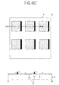
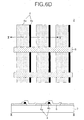
- FIGs. 6A to 6F are plan views and sectional views representing a method of manufacturing the organic electro-luminescence display device according to the present invention.
- FIGs. 7A and 7B are sectional views illustrating a taper angle of a bus electrode in accordance with a temperature of an etchant.
- FIG. 3 is a plan view illustrating an organic electro-luminescence display device according to the present invention
- FIG. 4 is a sectional view illustrating the organic electro-luminescence display device taken along a line II-II' in FIG. 3.
- the related art electro-luminescence display device includes an insulating film 6, a barrier rib 8, and an organic layer 10 formed between an anode electrode 4 and a cathode electrode 10, which are insulated from each other and crossing each other on a substrate 2.
- a plurality of anode electrodes 4 is provided on the substrate 2 in such a manner to be spaced at a predetermined distance from each other.
- a first driving signal is supplied to such the anode electrode 4 in order to emit an electron (or hole).
- the anode electrode 4 includes: a transparent electrode 4a made of a transparent conductive material, e.g., indium-tin-oxide ITO, etc., on a substrate 2; and a bus electrode 4b made of chrome Cr, molybdenum Mo, copper Cu, and etc. on one side of the transparent electrode 4a to compensate a resistance component of the transparent electrode 4a.
- the anode electrode 4 may include: a bus electrode 4b formed on a substrate 2; and a transparent electrode 4a formed on the substrate 2 having the bus electrode 4b.
- the bus electrode 4b is formed to have a relatively smooth inclination angle of about 30° to 70°.
- the bus electrode 4b is formed to have the inclination angle of about 30° to 50°
- the insulating film 6 is formed in a lattice type so as to expose an aperture for each EL cell area on the substrate 2 having the anode electrode 4.
- the barrier rib 8 is formed in a direction crossing the anode electrode 4, and is formed in parallel to the cathode electrode 12 by a predetermined distance to partition adjacent EL cells. In other words, the barrier rib 8 separates the organic layers 10 from each other and the cathode electrodes 12 from each other between the adjacent EL cells. Further, the barrier rib 8 has an overhang structure in which the upper portion thereof has a larger width than the lower portion thereof.
- the organic layer 10 is made of an organic compound on the insulating film 6.
- the organic layer 10 is formed by depositing a hole carrier layer, a light-emitting layer and an electron carrier layer onto the insulating film 6.
- a plurality of cathode electrodes 12 is provided on the organic layer 10 in such a manner to be spaced at a predetermined distance from each other, and in such a manner to be crossed with the anode electrodes 4.
- a second driving signal is supplied to the cathode electrode 12 in order to emit a hole (or electron).
- the bus electrode 4b is formed to have an inclination angle of 30° to 70°. Accordingly, a taper of the bus electrode 4b having a relatively smooth inclination angle becomes improved, so that a step coverage of the insulating film 6 formed to cover the bus electrode 4b becomes improved. Thus, it is possible to prevent an insulation breakdown.
- FIGs. 6A to 6F are plan views and sectional views representing a method of manufacturing the organic electro-luminescence display device according to the present invention.
- a transparent conductive material e.g., indium-tin-oxide, etc.
- a transparent electrode 4a of an anode electrode is deposited and then patterned on a substrate 2, to thereby form a transparent electrode 4a of an anode electrode on the substrate as shown in FIG. 6.
- Chrome Cr or Molybdenum Mo, etc. is deposited on the substrate 2 having the transparent electrode 4a and then is patterned by a photolithography process and an etching process using an etchant consisted of phosphoric acid in a range of 55 to 60 weight %, nitric acid in a range of 10 to 12 weight %, acetic acid in a range of 8 to 10 weight %, and water in a range of 18 to 27 weight %, to thereby form a bus electrode 4b of an anode electrode having a taper angle of 30° to 70° as shown in FIG. 6B.
- the etching process of the bus electrode 4b will be described in detail later.
- a photosensitive insulating material is deposited and then patterned on the substrate 2 having the anode electrode 4, to thereby form a insulating film 6 as shown in FIG. 6C.
- the insulating film 6 is formed in a lattice type at an entire portion except for a light-emitting portion.
- a photosensitive insulating material is deposited and then patterned on the substrate 2 having the insulating film 6, to thereby form a barrier rib 8 as shown in FIG. 6D.
- the barrier rib 8 is formed with a predetermined distance from adjacent barrier ribs in a direction crossing the anode electrode 4, and is formed at a non-light emitting portion.
- the organic layer 10 is formed on the substrate having the barrier rib 8 as shown in FIG. 6E.
- the organic layer 10 includes hole carrier layer, a light emitting layer, and an electron carrier layer.
- a cathode electrode 12 is formed on the substrate 2 having the organic layer 10 as shown in FIG. 6F. At this time, the cathode electrode 12 is entirely deposited to be formed, but is separated for each EL cell by the barrier rib having a relatively high height to be formed.
- the bus electrode 4b of the anode electrode according to the present invention is formed with result that a metal such as chrome Cr, molybdenum Mo, copper Cu, etc. is etched by an anisotropic etching manner using an etchant consisted of compositions shown in table 1, at a temperature of a normal temperature to 45°C, preferably temperature of about 30°C to 35°C.
- the bus electrode 4b formed by the etching manner using the etchant has an inclination angle of 30° to 70°.
- Phosphoric acid Nitric acid Acetic acid Water Composition content (wight%) 55 to 60 10 to 12 8 to 10 18 to 28
- a content of nitric acid becomes larger by about double amount than that of the related art, so that an etching speed of a metal making the bus electrode 4b becomes slower. Accordingly, the bus electrode 4b can be formed with an inclination angle smaller than that of the related art.
- an etching amount and inclination angle of the bus electrode 4b formed by the etchant shown in Table 1 are differentiated depending upon a temperature of the etchant as shown in Table 2.
- the bus electrode 4b located at a first location(near upper corner of right side in the substrate) is etched by about 0.54 ⁇ m from end of a photo-resist pattern 30 formed by an etching process and a developing process as shown in FIG. 7A
- the bus electrode 4b located at a second location(near center of the substrate) is etched by about 0.44 ⁇ m from end of the photo-resist pattern 30
- the bus electrode 4b located at a third location(near lower corner of left side of the substrate) is etched by about 0.52 ⁇ m from end of the photo-resist pattern 30.
- the bus electrode 4b is over-etched by a first width d1 from end of the photo-resist pattern 30 and the bus electrode 4b has a inclination angle ⁇ of about 54° to 63°.
- the bus electrode 4b located at a first location(near upper corner of right side in the substrate) is etched by about 0.20 ⁇ m from end of a photo-resist pattern 30 formed by an etching process and a developing process as shown in FIG. 7B
- the bus electrode 4b located at a second location(near center of the substrate) is etched by about 0.21 ⁇ m from end of the photo-resist pattern 30, and the bus electrode 4b located at a third location(near lower corner of left side of the substrate) is etched by about 0.28 ⁇ m from end of the photo-resist pattern 30.
- the bus electrode 4b is over-etched by a second width shorter than the first width d1, from end of the photo-resist pattern 30, and the bus electrode 4b has a inclination angle ⁇ of about 40° to 49°.
- the bus electrode is formed to have the inclination angle of 30° to 70°. Accordingly, the taper of the bus electrode having a relatively smooth inclination angle becomes improved, so that a step coverage of the insulating film formed to cover the bus electrode becomes improved. Thus, it is possible to prevent an insulation breakdown.
Landscapes
- Physics & Mathematics (AREA)
- Optics & Photonics (AREA)
- Electroluminescent Light Sources (AREA)
- Illuminated Signs And Luminous Advertising (AREA)
Applications Claiming Priority (2)
| Application Number | Priority Date | Filing Date | Title |
|---|---|---|---|
| KR2004019684 | 2004-03-23 | ||
| KR1020040019684A KR100620849B1 (ko) | 2004-03-23 | 2004-03-23 | 유기 전계 발광 소자 및 그 제조방법 |
Publications (2)
| Publication Number | Publication Date |
|---|---|
| EP1580824A1 true EP1580824A1 (de) | 2005-09-28 |
| EP1580824B1 EP1580824B1 (de) | 2008-05-14 |
Family
ID=34858875
Family Applications (1)
| Application Number | Title | Priority Date | Filing Date |
|---|---|---|---|
| EP05005803A Expired - Lifetime EP1580824B1 (de) | 2004-03-23 | 2005-03-17 | Organische elektrolumineszente Anzeigevorrichtung und deren Herstellungsverfahren |
Country Status (7)
| Country | Link |
|---|---|
| US (1) | US7825593B2 (de) |
| EP (1) | EP1580824B1 (de) |
| JP (1) | JP2005276828A (de) |
| KR (1) | KR100620849B1 (de) |
| CN (1) | CN1674753A (de) |
| AT (1) | ATE395720T1 (de) |
| DE (1) | DE602005006645D1 (de) |
Cited By (1)
| Publication number | Priority date | Publication date | Assignee | Title |
|---|---|---|---|---|
| WO2010038181A1 (en) * | 2008-10-02 | 2010-04-08 | Philips Intellectual Property & Standards Gmbh | Oled device with covered shunt line |
Families Citing this family (14)
| Publication number | Priority date | Publication date | Assignee | Title |
|---|---|---|---|---|
| JP5122731B2 (ja) * | 2005-06-01 | 2013-01-16 | 信越半導体株式会社 | 貼り合わせウェーハの製造方法 |
| KR100962436B1 (ko) * | 2008-05-07 | 2010-06-14 | 엘지전자 주식회사 | 디스플레이 패널 |
| JP5035198B2 (ja) * | 2008-09-26 | 2012-09-26 | 大日本印刷株式会社 | 有機エレクトロルミネッセンス素子およびその製造方法 |
| JP5709422B2 (ja) * | 2010-07-14 | 2015-04-30 | Necライティング株式会社 | 有機エレクトロルミネッセンス照明装置及びその製造方法 |
| KR20120119091A (ko) * | 2011-04-20 | 2012-10-30 | 삼성디스플레이 주식회사 | 유기 발광 표시 장치와, 이의 제조 방법 |
| US8674377B2 (en) | 2011-08-30 | 2014-03-18 | General Electric Company | Optoelectronic device package, array and method of fabrication |
| JP2014182918A (ja) * | 2013-03-19 | 2014-09-29 | Pioneer Electronic Corp | 発光素子および発光素子の製造方法 |
| WO2015047054A1 (ko) | 2013-09-30 | 2015-04-02 | 주식회사 엘지화학 | 유기 발광 소자의 제조방법 |
| KR101578620B1 (ko) * | 2013-09-30 | 2015-12-17 | 주식회사 엘지화학 | 적층체 및 이의 제조방법 |
| TW201526330A (zh) | 2013-09-30 | 2015-07-01 | Lg Chemical Ltd | 有機發光裝置 |
| JPWO2017119068A1 (ja) * | 2016-01-05 | 2018-10-25 | パイオニア株式会社 | 発光装置 |
| JP2018137084A (ja) * | 2017-02-21 | 2018-08-30 | 株式会社東海理化電機製作所 | 有機el表示装置及びその製造方法 |
| KR102946772B1 (ko) | 2020-11-30 | 2026-03-31 | 엘지디스플레이 주식회사 | 전계발광 표시장치 |
| DE102022116468B3 (de) | 2022-07-01 | 2022-12-29 | Cellforce Group Gmbh | Reinraumanordnung sowie Verfahren zur schnellen Bereitstellung eines Reinraumes und Verwendung der Reinraumanordnung |
Citations (3)
| Publication number | Priority date | Publication date | Assignee | Title |
|---|---|---|---|---|
| JPH10106751A (ja) * | 1996-09-30 | 1998-04-24 | Nec Corp | 有機薄膜エレクトロルミネッセンス表示装置の電極構造 |
| WO2003026012A2 (en) * | 2001-09-19 | 2003-03-27 | Osram Opto Semiconductors Gmbh | Organic light emitting diode light source |
| WO2003075616A1 (en) * | 2002-03-04 | 2003-09-12 | Rohm Co., Ltd. | Organic el display panel comprising electrode separator and its manufacturing method |
Family Cites Families (8)
| Publication number | Priority date | Publication date | Assignee | Title |
|---|---|---|---|---|
| TW364275B (en) * | 1996-03-12 | 1999-07-11 | Idemitsu Kosan Co | Organic electroluminescent element and organic electroluminescent display device |
| KR100273848B1 (ko) | 1996-09-30 | 2000-12-15 | 김영남 | 평판소자의 전극 |
| US6333518B1 (en) | 1997-08-26 | 2001-12-25 | Lg Electronics Inc. | Thin-film transistor and method of making same |
| JP2000091083A (ja) * | 1998-09-09 | 2000-03-31 | Sony Corp | 有機elディスプレイ |
| JP3893936B2 (ja) | 2001-10-19 | 2007-03-14 | セイコーエプソン株式会社 | ヘッドユニットのアライメントマスクおよびこれがセット可能なヘッドユニットの組立装置 |
| JP2003127397A (ja) * | 2001-10-26 | 2003-05-08 | Canon Inc | 回路基板の製造方法 |
| KR100859524B1 (ko) * | 2002-07-11 | 2008-09-22 | 삼성전자주식회사 | 박막 트랜지스터 기판 |
| CN102522509B (zh) * | 2002-08-02 | 2016-01-20 | 出光兴产株式会社 | 溅射靶、烧结体及利用它们制造的导电膜、有机el元件及其所用的衬底 |
-
2004
- 2004-03-23 KR KR1020040019684A patent/KR100620849B1/ko not_active Expired - Fee Related
-
2005
- 2005-03-15 JP JP2005073352A patent/JP2005276828A/ja active Pending
- 2005-03-17 AT AT05005803T patent/ATE395720T1/de not_active IP Right Cessation
- 2005-03-17 DE DE602005006645T patent/DE602005006645D1/de not_active Expired - Lifetime
- 2005-03-17 EP EP05005803A patent/EP1580824B1/de not_active Expired - Lifetime
- 2005-03-18 CN CNA2005100548110A patent/CN1674753A/zh active Pending
- 2005-03-21 US US11/084,791 patent/US7825593B2/en active Active
Patent Citations (4)
| Publication number | Priority date | Publication date | Assignee | Title |
|---|---|---|---|---|
| JPH10106751A (ja) * | 1996-09-30 | 1998-04-24 | Nec Corp | 有機薄膜エレクトロルミネッセンス表示装置の電極構造 |
| WO2003026012A2 (en) * | 2001-09-19 | 2003-03-27 | Osram Opto Semiconductors Gmbh | Organic light emitting diode light source |
| WO2003075616A1 (en) * | 2002-03-04 | 2003-09-12 | Rohm Co., Ltd. | Organic el display panel comprising electrode separator and its manufacturing method |
| US20050116629A1 (en) * | 2002-03-04 | 2005-06-02 | Makoto Takamura | Organic el display panel comprising electrode separator and its manufacturing method |
Non-Patent Citations (1)
| Title |
|---|
| PATENT ABSTRACTS OF JAPAN vol. 1998, no. 09 31 July 1998 (1998-07-31) * |
Cited By (2)
| Publication number | Priority date | Publication date | Assignee | Title |
|---|---|---|---|---|
| WO2010038181A1 (en) * | 2008-10-02 | 2010-04-08 | Philips Intellectual Property & Standards Gmbh | Oled device with covered shunt line |
| CN102171851B (zh) * | 2008-10-02 | 2014-05-07 | 皇家飞利浦电子股份有限公司 | 具有被覆盖的分流线的oled器件 |
Also Published As
| Publication number | Publication date |
|---|---|
| US7825593B2 (en) | 2010-11-02 |
| JP2005276828A (ja) | 2005-10-06 |
| EP1580824B1 (de) | 2008-05-14 |
| KR100620849B1 (ko) | 2006-09-13 |
| KR20050094529A (ko) | 2005-09-28 |
| CN1674753A (zh) | 2005-09-28 |
| ATE395720T1 (de) | 2008-05-15 |
| DE602005006645D1 (de) | 2008-06-26 |
| US20050212415A1 (en) | 2005-09-29 |
Similar Documents
| Publication | Publication Date | Title |
|---|---|---|
| CN110911461B (zh) | Oled显示面板及其制作方法 | |
| KR101961190B1 (ko) | 유기전압 발광소자 및 이의 제조방법 | |
| US7825593B2 (en) | Organic electro-luminescence display device and method of fabricating the same | |
| CN106847867B (zh) | 有机电致发光显示器件及其制备方法和显示装置 | |
| KR20040050945A (ko) | 유기 발광 표시판 | |
| US6781293B2 (en) | Organic EL device with high contrast ratio and method for manufacturing the same | |
| CN102299167A (zh) | 有机发光装置及其制造方法 | |
| CN110137225A (zh) | Oled显示面板及其制备方法 | |
| EP1724854B1 (de) | Organische elektrolumineszente Vorrichtung und Herstellungsverfahren | |
| KR20060023180A (ko) | 유기 el 패널 및 그 제조 방법 | |
| CN119816109B (zh) | 显示面板及其制作方法和显示装置 | |
| JPH11135257A (ja) | 有機エレクトロルミネッセンス素子の製造方法 | |
| KR100612118B1 (ko) | 다층 구조의 격벽 구조물을 포함하는 유기 전계발광소자및 그의 제조 방법 | |
| JP2006128110A (ja) | 有機電界発光表示素子及びその製造方法 | |
| KR100592388B1 (ko) | 유기 전계발광 표시소자 및 그 제조방법 | |
| US8564194B2 (en) | Organic light emitting diode device and method for fabricating the same | |
| KR20100064868A (ko) | 유기전계 발광소자 및 그 제조방법 | |
| CN114613918A (zh) | 显示面板与显示装置 | |
| KR101171116B1 (ko) | 유기발광소자 및 그 제조방법 | |
| US20240224710A1 (en) | Display panel and manufacturing method thereof | |
| KR100592387B1 (ko) | 일렉트로-루미네센스 표시 패널 및 그 제조 방법 | |
| KR100768711B1 (ko) | 유기 전계 발광 소자 및 그 제조방법 | |
| KR100696593B1 (ko) | 유기 전계발광 표시소자 및 그 제조방법 | |
| CN100553010C (zh) | 有机el元件以及制造方法 | |
| KR101054531B1 (ko) | 유기발광소자 및 그 제조 방법 |
Legal Events
| Date | Code | Title | Description |
|---|---|---|---|
| PUAI | Public reference made under article 153(3) epc to a published international application that has entered the european phase |
Free format text: ORIGINAL CODE: 0009012 |
|
| 17P | Request for examination filed |
Effective date: 20050317 |
|
| AK | Designated contracting states |
Kind code of ref document: A1 Designated state(s): AT BE BG CH CY CZ DE DK EE ES FI FR GB GR HU IE IS IT LI LT LU MC NL PL PT RO SE SI SK TR |
|
| AX | Request for extension of the european patent |
Extension state: AL BA HR LV MK YU |
|
| AKX | Designation fees paid |
Designated state(s): AT BE BG CH CY CZ DE DK EE ES FI FR GB GR HU IE IS IT LI LT LU MC NL PL PT RO SE SI SK TR |
|
| GRAP | Despatch of communication of intention to grant a patent |
Free format text: ORIGINAL CODE: EPIDOSNIGR1 |
|
| RIC1 | Information provided on ipc code assigned before grant |
Ipc: H01L 51/56 20060101ALI20071122BHEP Ipc: H01L 51/52 20060101AFI20071122BHEP |
|
| GRAS | Grant fee paid |
Free format text: ORIGINAL CODE: EPIDOSNIGR3 |
|
| GRAA | (expected) grant |
Free format text: ORIGINAL CODE: 0009210 |
|
| AK | Designated contracting states |
Kind code of ref document: B1 Designated state(s): AT BE BG CH CY CZ DE DK EE ES FI FR GB GR HU IE IS IT LI LT LU MC NL PL PT RO SE SI SK TR |
|
| REG | Reference to a national code |
Ref country code: GB Ref legal event code: FG4D |
|
| REG | Reference to a national code |
Ref country code: CH Ref legal event code: EP |
|
| REG | Reference to a national code |
Ref country code: IE Ref legal event code: FG4D Free format text: LANGUAGE OF EP DOCUMENT: FRENCH |
|
| REF | Corresponds to: |
Ref document number: 602005006645 Country of ref document: DE Date of ref document: 20080626 Kind code of ref document: P |
|
| PG25 | Lapsed in a contracting state [announced via postgrant information from national office to epo] |
Ref country code: SI Free format text: LAPSE BECAUSE OF FAILURE TO SUBMIT A TRANSLATION OF THE DESCRIPTION OR TO PAY THE FEE WITHIN THE PRESCRIBED TIME-LIMIT Effective date: 20080514 |
|
| PG25 | Lapsed in a contracting state [announced via postgrant information from national office to epo] |
Ref country code: ES Free format text: LAPSE BECAUSE OF FAILURE TO SUBMIT A TRANSLATION OF THE DESCRIPTION OR TO PAY THE FEE WITHIN THE PRESCRIBED TIME-LIMIT Effective date: 20080825 Ref country code: FI Free format text: LAPSE BECAUSE OF FAILURE TO SUBMIT A TRANSLATION OF THE DESCRIPTION OR TO PAY THE FEE WITHIN THE PRESCRIBED TIME-LIMIT Effective date: 20080514 |
|
| PG25 | Lapsed in a contracting state [announced via postgrant information from national office to epo] |
Ref country code: PL Free format text: LAPSE BECAUSE OF FAILURE TO SUBMIT A TRANSLATION OF THE DESCRIPTION OR TO PAY THE FEE WITHIN THE PRESCRIBED TIME-LIMIT Effective date: 20080514 Ref country code: AT Free format text: LAPSE BECAUSE OF FAILURE TO SUBMIT A TRANSLATION OF THE DESCRIPTION OR TO PAY THE FEE WITHIN THE PRESCRIBED TIME-LIMIT Effective date: 20080514 |
|
| PG25 | Lapsed in a contracting state [announced via postgrant information from national office to epo] |
Ref country code: IS Free format text: LAPSE BECAUSE OF FAILURE TO SUBMIT A TRANSLATION OF THE DESCRIPTION OR TO PAY THE FEE WITHIN THE PRESCRIBED TIME-LIMIT Effective date: 20080914 |
|
| PG25 | Lapsed in a contracting state [announced via postgrant information from national office to epo] |
Ref country code: LT Free format text: LAPSE BECAUSE OF FAILURE TO SUBMIT A TRANSLATION OF THE DESCRIPTION OR TO PAY THE FEE WITHIN THE PRESCRIBED TIME-LIMIT Effective date: 20080514 Ref country code: CZ Free format text: LAPSE BECAUSE OF FAILURE TO SUBMIT A TRANSLATION OF THE DESCRIPTION OR TO PAY THE FEE WITHIN THE PRESCRIBED TIME-LIMIT Effective date: 20080514 Ref country code: SE Free format text: LAPSE BECAUSE OF FAILURE TO SUBMIT A TRANSLATION OF THE DESCRIPTION OR TO PAY THE FEE WITHIN THE PRESCRIBED TIME-LIMIT Effective date: 20080814 Ref country code: DK Free format text: LAPSE BECAUSE OF FAILURE TO SUBMIT A TRANSLATION OF THE DESCRIPTION OR TO PAY THE FEE WITHIN THE PRESCRIBED TIME-LIMIT Effective date: 20080514 Ref country code: PT Free format text: LAPSE BECAUSE OF FAILURE TO SUBMIT A TRANSLATION OF THE DESCRIPTION OR TO PAY THE FEE WITHIN THE PRESCRIBED TIME-LIMIT Effective date: 20081014 |
|
| PG25 | Lapsed in a contracting state [announced via postgrant information from national office to epo] |
Ref country code: BE Free format text: LAPSE BECAUSE OF FAILURE TO SUBMIT A TRANSLATION OF THE DESCRIPTION OR TO PAY THE FEE WITHIN THE PRESCRIBED TIME-LIMIT Effective date: 20080514 Ref country code: RO Free format text: LAPSE BECAUSE OF FAILURE TO SUBMIT A TRANSLATION OF THE DESCRIPTION OR TO PAY THE FEE WITHIN THE PRESCRIBED TIME-LIMIT Effective date: 20080514 Ref country code: SK Free format text: LAPSE BECAUSE OF FAILURE TO SUBMIT A TRANSLATION OF THE DESCRIPTION OR TO PAY THE FEE WITHIN THE PRESCRIBED TIME-LIMIT Effective date: 20080514 |
|
| PLBE | No opposition filed within time limit |
Free format text: ORIGINAL CODE: 0009261 |
|
| STAA | Information on the status of an ep patent application or granted ep patent |
Free format text: STATUS: NO OPPOSITION FILED WITHIN TIME LIMIT |
|
| 26N | No opposition filed |
Effective date: 20090217 |
|
| PG25 | Lapsed in a contracting state [announced via postgrant information from national office to epo] |
Ref country code: BG Free format text: LAPSE BECAUSE OF FAILURE TO SUBMIT A TRANSLATION OF THE DESCRIPTION OR TO PAY THE FEE WITHIN THE PRESCRIBED TIME-LIMIT Effective date: 20080814 Ref country code: EE Free format text: LAPSE BECAUSE OF FAILURE TO SUBMIT A TRANSLATION OF THE DESCRIPTION OR TO PAY THE FEE WITHIN THE PRESCRIBED TIME-LIMIT Effective date: 20080514 |
|
| PG25 | Lapsed in a contracting state [announced via postgrant information from national office to epo] |
Ref country code: IT Free format text: LAPSE BECAUSE OF FAILURE TO SUBMIT A TRANSLATION OF THE DESCRIPTION OR TO PAY THE FEE WITHIN THE PRESCRIBED TIME-LIMIT Effective date: 20080514 |
|
| PG25 | Lapsed in a contracting state [announced via postgrant information from national office to epo] |
Ref country code: MC Free format text: LAPSE BECAUSE OF NON-PAYMENT OF DUE FEES Effective date: 20090331 |
|
| REG | Reference to a national code |
Ref country code: CH Ref legal event code: PL |
|
| REG | Reference to a national code |
Ref country code: IE Ref legal event code: MM4A |
|
| PG25 | Lapsed in a contracting state [announced via postgrant information from national office to epo] |
Ref country code: LI Free format text: LAPSE BECAUSE OF NON-PAYMENT OF DUE FEES Effective date: 20090331 Ref country code: IE Free format text: LAPSE BECAUSE OF NON-PAYMENT OF DUE FEES Effective date: 20090317 Ref country code: CH Free format text: LAPSE BECAUSE OF NON-PAYMENT OF DUE FEES Effective date: 20090331 |
|
| PG25 | Lapsed in a contracting state [announced via postgrant information from national office to epo] |
Ref country code: GR Free format text: LAPSE BECAUSE OF FAILURE TO SUBMIT A TRANSLATION OF THE DESCRIPTION OR TO PAY THE FEE WITHIN THE PRESCRIBED TIME-LIMIT Effective date: 20080815 |
|
| PG25 | Lapsed in a contracting state [announced via postgrant information from national office to epo] |
Ref country code: LU Free format text: LAPSE BECAUSE OF NON-PAYMENT OF DUE FEES Effective date: 20090317 |
|
| PGFP | Annual fee paid to national office [announced via postgrant information from national office to epo] |
Ref country code: FR Payment date: 20110317 Year of fee payment: 7 Ref country code: NL Payment date: 20110317 Year of fee payment: 7 |
|
| PG25 | Lapsed in a contracting state [announced via postgrant information from national office to epo] |
Ref country code: HU Free format text: LAPSE BECAUSE OF FAILURE TO SUBMIT A TRANSLATION OF THE DESCRIPTION OR TO PAY THE FEE WITHIN THE PRESCRIBED TIME-LIMIT Effective date: 20081115 |
|
| PGFP | Annual fee paid to national office [announced via postgrant information from national office to epo] |
Ref country code: DE Payment date: 20110309 Year of fee payment: 7 Ref country code: GB Payment date: 20110316 Year of fee payment: 7 |
|
| PG25 | Lapsed in a contracting state [announced via postgrant information from national office to epo] |
Ref country code: TR Free format text: LAPSE BECAUSE OF FAILURE TO SUBMIT A TRANSLATION OF THE DESCRIPTION OR TO PAY THE FEE WITHIN THE PRESCRIBED TIME-LIMIT Effective date: 20080514 |
|
| PG25 | Lapsed in a contracting state [announced via postgrant information from national office to epo] |
Ref country code: CY Free format text: LAPSE BECAUSE OF FAILURE TO SUBMIT A TRANSLATION OF THE DESCRIPTION OR TO PAY THE FEE WITHIN THE PRESCRIBED TIME-LIMIT Effective date: 20080514 |
|
| REG | Reference to a national code |
Ref country code: NL Ref legal event code: V1 Effective date: 20121001 |
|
| GBPC | Gb: european patent ceased through non-payment of renewal fee |
Effective date: 20120317 |
|
| REG | Reference to a national code |
Ref country code: FR Ref legal event code: ST Effective date: 20121130 |
|
| PG25 | Lapsed in a contracting state [announced via postgrant information from national office to epo] |
Ref country code: FR Free format text: LAPSE BECAUSE OF NON-PAYMENT OF DUE FEES Effective date: 20120402 Ref country code: GB Free format text: LAPSE BECAUSE OF NON-PAYMENT OF DUE FEES Effective date: 20120317 |
|
| REG | Reference to a national code |
Ref country code: DE Ref legal event code: R119 Ref document number: 602005006645 Country of ref document: DE Effective date: 20121002 |
|
| PG25 | Lapsed in a contracting state [announced via postgrant information from national office to epo] |
Ref country code: NL Free format text: LAPSE BECAUSE OF NON-PAYMENT OF DUE FEES Effective date: 20121001 |
|
| PG25 | Lapsed in a contracting state [announced via postgrant information from national office to epo] |
Ref country code: DE Free format text: LAPSE BECAUSE OF NON-PAYMENT OF DUE FEES Effective date: 20121002 |