EP1580080A1 - Seating sensor having film switch and resistor element - Google Patents
Seating sensor having film switch and resistor element Download PDFInfo
- Publication number
- EP1580080A1 EP1580080A1 EP05006657A EP05006657A EP1580080A1 EP 1580080 A1 EP1580080 A1 EP 1580080A1 EP 05006657 A EP05006657 A EP 05006657A EP 05006657 A EP05006657 A EP 05006657A EP 1580080 A1 EP1580080 A1 EP 1580080A1
- Authority
- EP
- European Patent Office
- Prior art keywords
- film
- conductive wire
- side contact
- pair
- resistor element
- Prior art date
- Legal status (The legal status is an assumption and is not a legal conclusion. Google has not performed a legal analysis and makes no representation as to the accuracy of the status listed.)
- Granted
Links
- 241000238413 Octopus Species 0.000 claims abstract description 41
- 125000006850 spacer group Chemical group 0.000 claims description 50
- 238000000034 method Methods 0.000 claims description 10
- 230000008569 process Effects 0.000 claims description 10
- 230000004044 response Effects 0.000 claims description 6
- 230000008859 change Effects 0.000 abstract description 4
- 238000004519 manufacturing process Methods 0.000 description 9
- 230000004048 modification Effects 0.000 description 6
- 238000012986 modification Methods 0.000 description 6
- 238000010586 diagram Methods 0.000 description 4
- 238000005452 bending Methods 0.000 description 3
- 239000011347 resin Substances 0.000 description 3
- 229920005989 resin Polymers 0.000 description 3
- BQCADISMDOOEFD-UHFFFAOYSA-N Silver Chemical compound [Ag] BQCADISMDOOEFD-UHFFFAOYSA-N 0.000 description 2
- 239000002131 composite material Substances 0.000 description 2
- 238000010438 heat treatment Methods 0.000 description 2
- 229910052709 silver Inorganic materials 0.000 description 2
- 239000004332 silver Substances 0.000 description 2
- OKTJSMMVPCPJKN-UHFFFAOYSA-N Carbon Chemical compound [C] OKTJSMMVPCPJKN-UHFFFAOYSA-N 0.000 description 1
- 229910052799 carbon Inorganic materials 0.000 description 1
- 230000015556 catabolic process Effects 0.000 description 1
- 238000006243 chemical reaction Methods 0.000 description 1
- 238000005352 clarification Methods 0.000 description 1
- 230000000694 effects Effects 0.000 description 1
- 230000005611 electricity Effects 0.000 description 1
- 239000004744 fabric Substances 0.000 description 1
- 239000010985 leather Substances 0.000 description 1
- 239000011112 polyethylene naphthalate Substances 0.000 description 1
- 238000004080 punching Methods 0.000 description 1
- 230000005855 radiation Effects 0.000 description 1
- 238000011144 upstream manufacturing Methods 0.000 description 1
Images


Classifications
-
- B—PERFORMING OPERATIONS; TRANSPORTING
- B60—VEHICLES IN GENERAL
- B60R—VEHICLES, VEHICLE FITTINGS, OR VEHICLE PARTS, NOT OTHERWISE PROVIDED FOR
- B60R21/00—Arrangements or fittings on vehicles for protecting or preventing injuries to occupants or pedestrians in case of accidents or other traffic risks
- B60R21/01—Electrical circuits for triggering passive safety arrangements, e.g. airbags, safety belt tighteners, in case of vehicle accidents or impending vehicle accidents
- B60R21/015—Electrical circuits for triggering passive safety arrangements, e.g. airbags, safety belt tighteners, in case of vehicle accidents or impending vehicle accidents including means for detecting the presence or position of passengers, passenger seats or child seats, and the related safety parameters therefor, e.g. speed or timing of airbag inflation in relation to occupant position or seat belt use
- B60R21/01512—Passenger detection systems
- B60R21/01516—Passenger detection systems using force or pressure sensing means
-
- B—PERFORMING OPERATIONS; TRANSPORTING
- B60—VEHICLES IN GENERAL
- B60N—SEATS SPECIALLY ADAPTED FOR VEHICLES; VEHICLE PASSENGER ACCOMMODATION NOT OTHERWISE PROVIDED FOR
- B60N2/00—Seats specially adapted for vehicles; Arrangement or mounting of seats in vehicles
- B60N2/002—Seats provided with an occupancy detection means mounted therein or thereon
-
- B—PERFORMING OPERATIONS; TRANSPORTING
- B60—VEHICLES IN GENERAL
- B60N—SEATS SPECIALLY ADAPTED FOR VEHICLES; VEHICLE PASSENGER ACCOMMODATION NOT OTHERWISE PROVIDED FOR
- B60N2/00—Seats specially adapted for vehicles; Arrangement or mounting of seats in vehicles
- B60N2/58—Seat coverings
- B60N2/5816—Seat coverings attachments thereof
- B60N2/5825—Seat coverings attachments thereof by hooks, staples, clips, snap fasteners or the like
-
- B—PERFORMING OPERATIONS; TRANSPORTING
- B60—VEHICLES IN GENERAL
- B60R—VEHICLES, VEHICLE FITTINGS, OR VEHICLE PARTS, NOT OTHERWISE PROVIDED FOR
- B60R21/00—Arrangements or fittings on vehicles for protecting or preventing injuries to occupants or pedestrians in case of accidents or other traffic risks
- B60R21/01—Electrical circuits for triggering passive safety arrangements, e.g. airbags, safety belt tighteners, in case of vehicle accidents or impending vehicle accidents
- B60R21/015—Electrical circuits for triggering passive safety arrangements, e.g. airbags, safety belt tighteners, in case of vehicle accidents or impending vehicle accidents including means for detecting the presence or position of passengers, passenger seats or child seats, and the related safety parameters therefor, e.g. speed or timing of airbag inflation in relation to occupant position or seat belt use
- B60R21/01512—Passenger detection systems
- B60R21/0153—Passenger detection systems using field detection presence sensors
- B60R21/01532—Passenger detection systems using field detection presence sensors using electric or capacitive field sensors
-
- B—PERFORMING OPERATIONS; TRANSPORTING
- B60—VEHICLES IN GENERAL
- B60R—VEHICLES, VEHICLE FITTINGS, OR VEHICLE PARTS, NOT OTHERWISE PROVIDED FOR
- B60R21/00—Arrangements or fittings on vehicles for protecting or preventing injuries to occupants or pedestrians in case of accidents or other traffic risks
- B60R21/01—Electrical circuits for triggering passive safety arrangements, e.g. airbags, safety belt tighteners, in case of vehicle accidents or impending vehicle accidents
- B60R21/015—Electrical circuits for triggering passive safety arrangements, e.g. airbags, safety belt tighteners, in case of vehicle accidents or impending vehicle accidents including means for detecting the presence or position of passengers, passenger seats or child seats, and the related safety parameters therefor, e.g. speed or timing of airbag inflation in relation to occupant position or seat belt use
- B60R21/01512—Passenger detection systems
- B60R21/0153—Passenger detection systems using field detection presence sensors
- B60R21/0154—Passenger detection systems using field detection presence sensors in combination with seat heating
-
- B—PERFORMING OPERATIONS; TRANSPORTING
- B60—VEHICLES IN GENERAL
- B60R—VEHICLES, VEHICLE FITTINGS, OR VEHICLE PARTS, NOT OTHERWISE PROVIDED FOR
- B60R21/00—Arrangements or fittings on vehicles for protecting or preventing injuries to occupants or pedestrians in case of accidents or other traffic risks
- B60R21/01—Electrical circuits for triggering passive safety arrangements, e.g. airbags, safety belt tighteners, in case of vehicle accidents or impending vehicle accidents
- B60R2021/01122—Prevention of malfunction
- B60R2021/01129—Problems or faults
- B60R2021/01136—Cut lines
-
- B—PERFORMING OPERATIONS; TRANSPORTING
- B60—VEHICLES IN GENERAL
- B60R—VEHICLES, VEHICLE FITTINGS, OR VEHICLE PARTS, NOT OTHERWISE PROVIDED FOR
- B60R21/00—Arrangements or fittings on vehicles for protecting or preventing injuries to occupants or pedestrians in case of accidents or other traffic risks
- B60R21/01—Electrical circuits for triggering passive safety arrangements, e.g. airbags, safety belt tighteners, in case of vehicle accidents or impending vehicle accidents
- B60R2021/01122—Prevention of malfunction
- B60R2021/01129—Problems or faults
- B60R2021/01143—Short circuits
Landscapes
- Engineering & Computer Science (AREA)
- Mechanical Engineering (AREA)
- Aviation & Aerospace Engineering (AREA)
- Transportation (AREA)
- Push-Button Switches (AREA)
- Seats For Vehicles (AREA)
Abstract
Description
- The present invention relates to a seating sensor provided to a seat of a vehicle for detecting presence or absence of an occupant on the seat.
- A seating sensor embedded in a seat of a vehicle for detecting presence or absence of an occupant is conventionally known. The seating sensor includes a resin film provided with film switches. The film switches are activated in response to sitting pressure applied by an occupant. The film switches are provided with conductive patterns that form conducting paths for supplying electric power to the film switches. Base end portions of the conductive patterns form connector terminals that are to be inserted into a vehicular side connector.
- A seating sensor disclosed in JP-A-11-297153 incorporates a break-detecting resistor, so that an internal disconnection failure in the seating sensor is capable of being detected. The conventional seating sensor with a break-detecting resistor is specifically described in reference to FIG. 16.
- A plus
source line 4a, a minus source line 4b, a break-detecting resistor element R1, and a number ofcontact electrode couples 30 are formed on the top surface of a lower film. The plussource line 4a and the minus source line 4b are generally twisted and turned, so that the plus andminus source lines 4a, 4b are spaced for a predetermined distance away from each other. The plus andminus source lines 4a, 4b are substantially in parallel with each other, and are widely distributed over the seated surface. The break-detecting resistor element R2 connects an end of the plussource line 4a with an end of the minus source line 4b. Thecontact electrode couples 30 are fixed contacts that respectively diverge from the plussource line 4a and minus source line 4b. The plussource line 4a and minus source line 4b face each other like comb teeth in thecontact electrode couples 30. Thecontact electrode couples 30, which are large in total number, are arranged throughout the plussource line 4a and minus source line 4b. - An upper film is arranged on the top surface of the lower film via spacers that is made of resin placed therebetween. Conductive patterns, which serve as movable contacts in the locations where the spacers are cut out, are printed on the bottom surface of the upper film. Thus, each movable contact touches a
contact electrode couples 30, when a seat is occupied, so that the plussource line 4a and minus source line 4b are short-circuited, Thereby, seating can be detected. That is, when the seating sensor is viewed as an electric circuit, a number of film switches, which are constructed of thecontact electrode couples 30 and movable contacts, are connected in parallel with the break-detecting resistor element R2. - As long as neither the plus
source line 4a nor minus source line 4b has a broken portion, resistance between the base end portions of the plussource line 4a and minus source line 4b is identical. That is, the electric resistance of the circuit, which is viewed from the connector terminals of the seating sensor, is identical. When the seat is not occupied, the electric resistance becomes the electric resistance of the break-detecting resistor element R2. - When the seat is occupied, the film switch is closed, so that the electric resistance of the circuit becomes significantly small. Here, the wiring resistance of the plus
source line 4a and minus source line 4b shall be ignored. Further, when the plussource line 4a or minus source line 4b has a broken portion, the electric resistance value viewed from the connector terminals of the seating sensor ideally reaches almost an infinitely large value. Therefore, a break in the plussource line 4a and minus source line 4b can be easily detected. - However, in the conventional seating sensor with a break-detecting resistor, the break-detecting resistor element needs to be provided away from the connector farther than all the film switches, when being viewed from the side of the connector. That is, the break-detecting resistor element needs to be provided on leading end portions of conductive wires in order to detect a break of the conductive wire, which results termination of supplying electric power to all the film switches. Accordingly, the conductive wire becomes difficult to be forked similarly to octopus legs. In addition, wires, which lead to the number of film switches arranged on the seated surface, may be elongated. Accordingly, influence of variations of wiring resistances on signal voltages becomes large depending on the positions where the film switches are arranged. That is, the resistance value of the seating sensor viewed from the side of the connector becomes small when the film switch nearest to the connector is in its on state, and the resistance value becomes large when the film switch nearest to the break-detecting resistor element is in its on state.
- Besides, stress concentration may arise in connecting portions between the break-detecting resistor element and conductive wires due to repeatedly seating in the conventional seating sensor. The connecting portions are arranged on the seated surface. Accordingly, the wires may easily break at the connecting portions. Additionally, application of pressure to the break-detecting resistor element causes a change in resistance of the break-detecting resistor element, in the conventional seating sensor.
- In view of the foregoing problems, it is an object of the present invention to provide a seating sensor that has a structure, in which a seating sensor performance of detecting a break can be protected from being degraded. It is another object of the present invention to provide a seating sensor that has a structure, in which a disconnection failure owing to addition of a break-detecting resistor element can be restricted.
- According to the resent invention, a seating sensor includes a film, a pair of conductive wires, multiple film switches, and a break-detecting resistor element.
- The film is electrically insulative. The pair of conductive wires is low in resistance. The pair of conductive wires is formed on the film. The pair of conductive wires has base end portions that are connected with a connector. The film switches detect sitting. The film switches are formed in the pair of conductive wires to short the pair of conductive wires in response to sitting. The break-detecting resistor element has predetermined electric resistance. The break-detecting resistor element is formed on the film. The break-detecting resistor element has ends that are individually connected with the pair of conductive wires. The break-detecting resistor element is located between the base end portions of the pair of conductive wires and the film switches.
- The seating sensor further includes a seated-surface-arranged portion and an exterior-seated-surface-arranged portion. The seated-surface-arranged portion includes the film switches. The seated-surface-arranged portion is arranged in a seated surface of a sitting space. The exterior-seated-surface-arranged portion includes the break-detecting resistor element. The exterior-seated-surface-arranged portion is arranged in a location, which is other than the seated surface, adjacent to the seated-surface-arranged portion. The break-detecting resistor element is arranged in the exterior-seated-surface-arranged portion.
- The break-detecting resistor element is arranged at a substantially central portion between an end portion of the film, which is on the side of the plurality of film switches, and the base end portions of the pair of conductive wires.
- The film includes a lower-side film, an upper-side film, and a spacer film. A plus conductive wire and a minus conductive wire are formed as the pair of conductive wires on the lower-side film. The plus conductive wire has a first lower-side contact of the plurality of film switches. The minus conductive wire has a second lower-side contact of the film switches. The first upper-side contact of the film switches, a second upper-side contact of the film switches, and a conductive wire are formed on the upper-side film, The first upper-side contact faces the first lower-side contact of the plus conductive wire. The second upper-side contact faces the second lower-side contacts of the minus conductive wire. The conductive wire connects the first upper-side contact with the second upper-side contact. The spacer film is electrically insulative. The spacer film is interposed between the lower-side film and the upper-side film. The spacer film defines an opening. The first lower-side contact is capable of making contact with the first upper-side contact through the opening of the spacer film. The second lower-side contact is capable of making contact with the second upper-side contact through the opening of the spacer film.
- The first lower-side contact branches from the plus conductive wire in a shape of octopus legs, and the second lower-side contact branches from the minus conductive wire in a shape of octopus legs.
- Specifically, the film includes the lower-side film, the upper-side film, and the spacer film. The spacer film is electrically insulative, and is interposed between the lower-side film and the upper-side film. Each film switch includes one of the first lower-side contact and the second lower-side contact that are formed on the lower-side film. Each film switch includes one of the first upper-side contact and the second upper-side contact that are formed on the upper-side film. Each first lower-side contact faces each first upper-side contact, and each second lower-side contact faces each second upper-side contact. The pair of conductive wires includes the plus conductive wire and the minus conductive wire that are formed on the lower-side film. The plus conductive wire is connected with each first lower-side contact, and the minus conductive wire is connected with each second lower-side contacts. The upper-side film includes the conductive wire that connects the first upper-side contact with the second upper-side contact. The spacer film defines an opening. Each first lower-side contact is capable of making contact with each first upper-side contact through the opening of the spacer film. Each second lower-side contact is capable of making contact with each second upper-side contact through the opening of the spacer film.
- Alternatively, the plus conductive wire has first lower-side contacts of the film switches. The minus conductive wire has second lower-side contacts of the film switches. Each first lower-side contact and each second lower-side contact are adjacent to each other. Upper-side contacts of the film switches are formed on the upper-side film. Each upper-side contact faces each first lower-side contact of the plus conductive wire and each second lower-side contact of the minus conductive wire. Each first lower-side contact and each second lower-side contact are capable of making contact with each upper-side contacts through the opening of the spacer film.
- Specifically, each film switch includes a first lower-side contact and a second lower-side contact that are formed on the lower-side film to be adjacent to each other. Each film switch includes an upper-side contact that is formed on the upper-side film. The upper-side contact faces both the first lower-side contact and the second lower-side contact that are adjacent to each other. The pair of conductive wires includes the plus conductive wire and the minus conductive wire that are formed on the lower-side film. The plus conductive wire is connected with each first lower-side contact, and the minus conductive wire is connected with each second lower-side contacts. The spacer film defines an opening, through which both the first lower-side contact and the second lower-side contact are capable of making contact with the upper-side contact.
- The seating sensor may include a current-limiting resistor element that limits current. The resistor element is located on the side of the base end portion of the pair of conductive wires with respect to the plurality of film switches. The current-limiting resistor element is arranged on the film. The current-limiting resistor element is connected in series with at least one of the pair of conductive wires.
- The current-limiting resistor element is manufactured in a printing process identical with a printing process in which the break-detecting resistor element is manufactured.
- The current-limiting resistor element is connected with at least one of the pair of conductive wires on the side of the base end portion of the pair of conductive wires with respect to the break-detecting resistor element.
- The film includes an octopus leg-shaped portion and a straight belt-shaped portion. The octopus leg-shaped portion includes film switches formed therein. The straight belt-shaped portion is arranged between the octopus leg-shaped portion and the connector. Each of the pair of conductive wires is formed in the octopus leg-shaped portion. The pair of conductive wires is substantially line symmetrical with respect to the straight belt-shaped portion as a central line thereof.
- The above and other objects, features and advantages of the present invention will become more apparent from the following detailed description made with reference to the accompanying drawings. In the drawings:
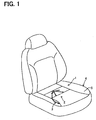
- FIG. 1 is a schematic perspective view showing a seating sensor provided to a seat according to a first embodiment of the present invention;
- FIG. 2 is a schematic plan view showing the seating sensor according to the first embodiment;
- FIG. 3 is a cross-sectional side view taken along the line III-III in FIG. 2 according to the first embodiment;
- FIG. 4 is an exploded plan view showing a lower-side film of the seating sensor according to the first embodiment;
- FIG 5 is an exploded plan view showing an upper-side film of the seating sensor according to the first embodiment;
- FIG. 6 is a cross-sectional side view showing the seating sensor, when the seat is not occupied, according to the first embodiment;
- FIG. 7 is a cross-sectional side view showing the seating sensor, when the seat is occupied, according to the first embodiment;
- FIG. 8 is an enlarged plan view showing a main part of the seating sensor according to the first embodiment;
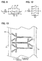
- FIG. 9 is an equivalent circuit diagram showing the seating sensor according to the first embodiment;
- FIG. 10 is an exploded plan view showing a lower-side film of a seating sensor according to the second embodiment of the present invention;
- FIG. 11 is an exploded plan view showing an upper-side film of the seating sensor according to the second embodiment;
- FIG 12 is an equivalent circuit diagram showing the seating sensor according to the second embodiment;
- FIG. 13 is a schematic plan view showing a baking process of the seating sensor according to the second embodiment;
- FIG. 14 is a block circuit diagram showing a sitting-detecting apparatus according to a third embodiment of the present invention;
- FIG. 15 is a block circuit diagram showing a sitting-detecting apparatus according to a modification of the third embodiment; and
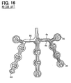
- FIG. 16 is a plan view showing a seating sensor according to a prior art.
-
- Preferred embodiments of a seating sensor of the present invention will be described below. However, the present invention is not limited to the embodiments below, and it is obvious that the technical idea of the present invention can be embodied by other known arts or a combination thereof.
- As shown in FIGS. 1 to 3, the
seating sensor 1 is formed by punching a film. Theseating sensor 1 includes an octopus leg-shapedportion 2 and astraight portion 3. - The octopus leg-shaped
portion 2 is formed in a shape like a group of octopus legs. Thestraight portion 3 linearly extends from the octopus leg-shapedportion 2. The octopus leg-shapedportion 2 and a part of thestraight portion 3, in which thestraight portion 3 is connected with the octopus leg-shapedportion 2, are arranged on the top surface, i.e. seated surface of a cushion 6 of theseat 5. Thereby, the octopus leg-shapedportion 2 and the part of thestraight portion 3 construct a seated-surface-arranged portion, which is arranged on the seated-surface of theseat 5. The top surface of a cushion 6 of theseat 5 is a seated portion of the sittingspace 4. As shown in FIG. 3, the remaining part of thestraight portion 3 extends through a gap of the cushion 6 of theseat 5 downward along a side face of the cushion 6. Aseat cover 7 is made of a cloth or leather for covering the cushion 6. Theseat cover 7 surrounds and covers theseating sensor 1 above the top surface of the cushion 6. Thestraight portion 3 of theseating sensor 1 protrudes from the bottom surface of theseat cover 7 on the bottom surface of the cushion 6. Thestraight portion 3 of theseating sensor 1 is attached to aconnector 300 fixed on the bottom surface of theseat 5. - As shown in FIGS. 6 and 7, the
seating sensor 1 includes a lower-side film (electrically irtsulative film) 8, an upper-side film (electrically insulative film) 9, aspacer film 10,conductive layers conductive layers spacer film 10 is formed of resin film, and is placed between the lower-side film and the upper-side film. Theconductive layers side film 8 by printing. Theconductive layers side film 9 by printing. Theconductive layers conductive layers - The
conductive layers side film 8 construct a plusconductive wire 15, a minusconductive wire 16, first and second lower-side contacts 21 of switches 17-20. As shown in FIG, 4, the first lower-side contacts 21 of the switches 17-20 are connected to the plusconductive wire 15, the second lower-side contacts 21 of the switches 17-20 are connected to the minusconductive wire 16. As shown in FIG. 5, theconductive layers side film 9 construct first and second upper-side contacts 22 of the switches 17-20 and aconductive wire 23. Theconductive wire 23 connects the first upper-side contacts 22 with second upper-side contacts 22. The first and second upper-side contacts 22 of the switches 17-20 are also serve as short contacts. Here, in FIGS. 4 and 5, the conductive wire is partially hatched for clarification of the illustrations. - The plus
conductive wire 15 and the minusconductive wire 16 are provided in thestraight portion 3 of theseating sensor 1 to be located apart from each other for a predetermined distance along the width direction of thestraight portion 3. As shown in FIG. 4, the plusconductive wire 15 and the minusconductive wire 16 extend to the base end portion of thestraight portion 3 in the longitudinal direction of thestraight portion 3. The plusconductive wire 15 and the minusconductive wire 16 construct terminals for connection of the connector at the base end portion. That is, the plusconductive wire 15 and the minusconductive wire 16 are inserted into theconnector 300, and are fixed to the base end portion of thestraight portion 3. - Each of the first and second lower-
side contacts 21 shown in FIG. 4 and the corresponding upper-side contacts 22 shown in FIG. 5 face each other via an opening of thespacer film 10 located therebetween as shown in FIGS. 6, 7. Each of the first and second lower-side contacts 21 are brought into contact with the corresponding upper-side contacts 22 on application of sitting pressure thereby to be electrically connected. It is obvious that theseating sensor 1 is turned on, when the film switches 17, 20 or the film switches 18, 19 turn on. - In FIG. 4, the current-limiting resistor element R1 and the break-detecting resistor element R2 are formed on the lower-
side film 8 through a common process. The current-limiting resistor element R1 is interposed in the plusconductive wire 15, and is located substantially at a central portion of thestraight portion 3. The break-detecting resistor element R2 is formed such that the resistor element R2 is located substantially at the central portion of thestraight portion 3. The break-detecting resistor element R2 connects the plusconductive wire 15 with the minusconductive wire 16. - As shown in FIGS. 8 and 9, when a predetermined voltage is applied between the paired base end portions of the
seating sensor 1 via a load resistance, and when theswitches switches seating sensor 1 is changed, so that seating can be detected. In addition, when a break arises on the upstream side of the break-detecting resistor element R2, voltage drop in theseating sensor 1 increases, so that the break can be detected. - The manufacturing process will be described below. The manufacturing process itself may be the same as that of the conventional seating sensor with a break-detecting resistor. As shown in FIG. 6, the lower-
side film 8 and the upper-side film 9 are formed of polyethylene naphthalate (PEN) films. The lower-side film 8. is printed with the paste forconductive layers side film 9 is printed with the paste forconductive layers side film 8 and upper-side film 9 are baked. Subsequently, aspacer film 10 is sandwiched and glued between the lower-side film 8 and the upper-side film 9, so that an elongated composite film is formed. The elongated composite film may be cut out into a form shown in FIG 1. The upper-side film 9 is removed in the base end portions of the plusconductive wire 15 and minusconductive wire 16. Theseating sensor 1 formed through the above process is glued on aseat 5, and the manufacturing process is completed. - The first and second lower-
side contacts 21 of theswitches conductive wire 15. Besides, the first and second lower-side contacts 21 of theswitches conductive wire 16. In the first and second lower-side contacts 21 having this structure, wiring voltage drop in the plusconductive wire 15 and minusconductive wire 16 can be reduced. - Specifically, according to the conventional structure of the seating sensor shown in FIG. 16, the
plus source line 4a and minus source line 4b are extended throughout the seating sensor without diverging. Therefore, wiring paths of theplus source line 4a and minus source line 4b in the conventional structure are elongated compared with the structure of the present invention, in which the plus and minusconductive wires - As shown in FIG. 10, a plus
conductive wire 15, a minusconductive wire 16, and first and second lower-side contacts side film 8. The first lower-side contacts 21a of the of switches 17-20 are connected to the plusconductive wire 15. The second lower-side contacts 21b of the of switches 17-20 are connected to the minusconductive wire 16. The second lower-side contacts 21 b of the switches 17-20 form octopus-legs-like lines, which diverge from the minusconductive wire 16, so that wiring voltage drop in the minusconductive wire 16 is reduced. In the switches 17-20, the first and second lower-side contacts - As shown in FIG. 11 and12, short contacts (upper-side contacts) 24 are formed on the upper-
side film 9. Eachshort contact 24 faces the corresponding first and second lower-side contacts short contact 24, theshort contact 24 is brought into contact with the first and second lower-side contacts - The baking process for the seating sensor of the first or second embodiment is described in reference to FIG. 13.
- An
elongated film 100 with a number ofseating sensors 1 printed thereon is moved into a baking furnace from its inlet to the outlet in the lengthwise direction thereof at a constant speed. Therefore, the baking furnace is formed to have a longer size in the longitudinal direction of theelongated film 100, i.e. the moving direction thereof. - The
elongated film 100 is arranged within side strips 101, 102 located inside of the baking furnace. The current-limiting resistor elements R1 and the break-detecting resistor elements R2 can be located substantially in a central portion between side strips 101, 102 in the baking furnace. That is, the current-limiting resistor elements R1 and the break-detecting resistor elements R2 can be located substantially in a central portion with respect to the direction of the width of theelongated film 100. Hence, variations in temperature and flow rate of heated gas supplied into the baking furnace are reduced. Besides, variations in radiation heat, which is applied to the resistor elements R1, R2 from the wall of the baking furnace, are reduced. As a result, variations in baking of the current-limiting resistor elements R1 and break-detecting resistor elements R2 are made smaller. Thereby, variations of grain radius and the like of the resistor elements R1, R2 caused due to variations in baking temperature and baking time, can be reduced. Thus, variations of the resistance values among the resistor elements R1, R2 can be reduced. - As described above in detail, the break-detecting resistor element R2 is arranged nearer to the connector than all the film switches 17-20 on the seated surface, dissimilarly to the conventional structure, Whereby, the degree of freedom of wiring can be increased such that the wire can be branched like octopus legs, for example. Consequently, wiring resistance and variations of wiring resistance can be reduced. In addition, the break-detecting resistor element R2 need not to be arranged on the seated surface of the
seat 5. Thereby, stress concentration owing to repeatedly seating in the connecting portions between the break-detecting resistor element R2 andconductive wires - Besides, the break-detecting resistor element R2 is formed in a location outside the seated surface of the film, and is formed away from the sitting-detecting film switches 17-20. The sitting-detecting film switches 17-20 are located on the seated surface of the sitting space, and are formed on the film, so that the seating sensor with the break-detecting resistor element R2 can be significantly restricted from causing a disconnection failure.
- Further, base end portions of the plus and minus
conductive wires side film 8, and then the break-detecting resistor element R2 can be formed by printing overlapping the plus and minusconductive wires - The embodiment relates to a sitting-detecting apparatus with the
seating sensor 1 of the second embodiment having the equivalent circuit shown in FIG. 12. Especially, a function of detecting a ground fault is imparted to the sitting-detecting apparatus. Besides, theseating sensor 1 of the first embodiment, which has the equivalent circuit shown in FIG. 9, may be used instead of theseating sensor 1 shown in FIG. 12. - A
controller 200 shown in FIG. 14 includes a built-in microcomputer. A constantcurrent source 201 supplies the high potential-side conductive wire 15 (FIG. 4) of theseating sensor 1 with predetermined constant current through an on-vehicle wiring harness 202 and aconnector 300. The low potential-sideconductive wire 16 of theseating sensor 1 is grounded via the on-vehicle wiring harness 202. - The
controller 200 incorporates an A/D converter for converting potential of the high potential-sideconductive wire 15 into a digital signal. The AID converter may have a multiplexer circuit in order to enable common use of a signal from another sensor for digital conversion. In the equivalent circuit of the seating sensor shown in FIG. 12, when any one of the sitting-detecting switches is in its on state, the resistance of theseating sensor 1 is substantially equal to the resistance value r1 of the current-limiting resistor R1. When all the sitting-detecting switches are in the off states, the resistance of theseating sensor 1 is substantially equal to the sum of the resistance value r1 of the current-limiting resistor element R1 and the resistance value r2 of the break-detecting resistor element R2. - Therefore, when the constant
current source 201 supplies constant current ic to theseating sensor 1, signal voltage Vs, which is equal to ic × r1 or ic × (r1 + r2), is input to thecontroller 200. Thereby, thecontroller 200 can discriminate between presence and absence of an occupied seat based on the changes of the signal voltage Vs. - The constant
current source 201 may break down, and may become unable to supply the constant current ic. Alternatively, a ground fault may occur in the on-vehicle wiring harness 202, which extends from the constantcurrent source 201 to theseating sensor 1, or in theconnector 300. In this situation, the signal voltage Vs reaches a value that is much smaller than the voltage resulting from ic × r1 or ic × (r1 + r2) described above. Specifically, the value of the signal voltage Vs becomes typically almost 0 volt, and becomes much smaller than the voltage, which results from ic × r1 or ic × (r1 + r2). Therefore, an accident of a ground fault in the circuit, which is between the power supply circuit system and theseating sensor 1, can be surely detected in the above structure, regardless of presence or absence of a seated occupant. - Meanwhile, when the
seating sensor 1 does not have a current-limiting resistor element R1 described above, the on-resistance value of theseating sensor 1 when the seat is occupied becomes very small, accordingly, the signal voltage Vs becomes excessively small. Thus, discriminating between seating and a ground fault becomes difficult. On the contrary, when theseating sensor 1 has only the current-limiting resistor element R1 without the break-detecting resistor element R2, the constantcurrent source 201 cannot supply constant current when the seat is not occupied. Further, when theseating sensor 1 has only the break-detecting resistor element R2 without the current-limiting resistor element R1, it becomes difficult to detect a ground fault when the seat is occupied for the reason above-mentioned. Specifically, when theseating sensor 1 has only the break-detecting resistor element R2 without the current-limiting resistor element R1, the on-resistance value of theseating sensor 1 when the seat is occupied becomes very small. - A modification is described in reference to FIG. 15. In this modification, a
constant voltage source 203 is used instead of the constantcurrent source 201 shown in FIG. 14. Theconstant voltage source 203 outputs constant voltage Vc, and the constant voltage Vc is applied to the high potential-sideconductive wire 15 of theseating sensor 1 via a load resistor RO, an on-vehicle wiring harness 202, and aconnector 300. The low potential-sideconductive wire 16 of theseating sensor 1 is grounded via the on-vehicle wiring harness 202. - In this structure, the signal voltage Vs becomes r1 x Vc / (ro + r1) or (r1 + r2) × Vc / (ro + r1 + r2), where the resistance value of the load resistor RO is represented by ro. Thus, the
controller 200 is capable of discriminating between presence and absence of an occupied seat based on the changes of the signal voltage Vs. - The
constant voltage source 203 may break down, and theconstant voltage source 203 may become unable to supply the constant voltage Vc. Alternatively, a ground fault may occur in the on-vehicle wiring harness 202, which extends from theconstant voltage source 203 to theseating sensor 1, or in theconnector 300. In this situation, the signal voltage Vs reaches a value much smaller than the voltage resulting from ic × r1 or ic × (r1 + r2) as described above. Specifically, the value of the signal voltage Vs is typically almost 0 volt that is much smaller than the voltage, which results from r1 x Vc / (ro + r1) or (r1 + r2) × Vc / (ro + r1 + r2). Therefore, an accident of a ground fault in the circuit, which is between the power supply circuit system and theseating sensor 1, can be surely detected in the above structure, regardless of presence or absence of a seated occupant. - According to the third embodiment and the modification thereof, a ground fault and a breakdown of the power source, which results in turning off the power source, can be discriminated regardless of presence or absence of an occupant. Moreover, such discrimination is performed using the current-limiting resistor element R1 and the break-detecting resistor element R2 of the
seating sensor 1 as the resistor elements needed for the discriminating operation. Therefore, an additional resistor element need not, and increase in manufacturing cost can be restricted. - That is, the above sitting-detecting apparatus has a power source circuit and a ground fault determining circuit. The power source circuit supplies predetermined current to the seating sensor. The ground fault determining circuit detects current flowing through the seating sensor, and detects voltage drop in the seating sensor, so that the ground fault determining circuit determines a ground fault in the seating sensor and a ground fault in an electricity supply route leading to the seating sensor, based on the detected current or voltage drop.
- In the above structure, the break-detecting resistor element R2 is arranged on the side of the
connector 300 with respect to all the film switches 17-20 on the seated surface in theseating sensor 1. Thereby, a degree of freedom of wiring can be increased, so that theconductive wires seating sensor 1 viewed from the side of theconnector 300 becomes small when the film switch nearest to theconnector 300 is in its on state, and becomes large when the film switch nearest to the break-detecting resistor element R2 is in its on state. That is, variations in the resistance value of theseating sensor 1 can be reduced. In addition, the break-detecting resistor element R2 need not to be arranged on the seated surface, so that the following two problems can be easily avoided. The first problem is that stress is concentrated owing to repeatedly seating in connecting portions between the break-detecting resistor element R2 andconductive wires wires - In the above structure, the break-detecting resistor element R2 connected in parallel with the film switches 17-20 is arranged on the side of the
connector 300 with respect to the film switches 17-20. In this structure, a break in theconductive wires seating sensor 1 includes afilm conductive wires film connector 300 for external connection. The base end portions of theconductive wires connector 300. With regard to the structure of the film-type seating sensor 1, theconductive wires film conductive wires connector 300. Therefore, bending stress, which is applied to thefilm film seating sensor 1 with the break-detecting resistor element R2 can be produced at low cost. Here, the break-detecting resistor element R2 can be formed on thefilm film conductive wires film - In the above structure, the break-detecting resistor element R2 is formed in a location outside the seated surface of the
film 8, and is formed in a location away from the sitting-detecting film switches 17-20. The sitting-detecting film switches 17-20 are located on the seated surface of the sittingspace 4, and are formed on thefilm seating sensor 1 can be significantly reduced. More specific description will be presented below. - In order to examine reliability of the
seating sensor 1 with a break-detecting resistor disclosed in JP-A-11-297153, a sensor including a resistor is set in a sitting space, and load is repeatedly applied to the sitting space. Theconductive wires space 4 for more than several thousands of times, a break is caused in a connecting portion between theconductive wires conductive wires conductive wires connector 300 with respect to the seated surface, and is arranged outside the seated surface, so that stress concentration is capable of being reduced. - The break-detecting resistor element R2 is arranged at a substantially central portion between the end portion of the
film seating sensor 1 is formed. Thereby, in the above arrangement, variations of the break-detecting resistor element R2 in temperature can be reduced in the heating process, so that variations in resistance value of the break-detecting resistor element R2 can be reduced. - In the first embodiment, the film includes the lower-
side film 8, the upper-side film 9, and the electrically insulative spacerfilm 10. The plus and the minusconductive wires side film 8. The plus and minusconductive wires side contacts 21 of the film switches 17-20. The upper-side film 9 has the upper-side contacts (first and second upper-side contacts) 22 of the film switches 17-20 and theconductive wire 23. The first upper-side contacts 22 of the film switches 19, 20 face the first lower-side contact 21 of the plusconductive wire 15. The second upper-side contact 22 of the film switches 17, 18 face the lower-side contacts 21 of the minusconductive wire 16. Theconductive wire 23 connects the first upper-side contact 22 with the second upper-side contact 22 formed on the upper-side film 9. The electrically insulative spacerfilm 10 has the opening, through which the lower-side contacts 21 are capable of making contact with the upper-side contacts 22. Thespacer film 10 is interposed between the lower-side film 8 and upper-side film 9. The lower-side contacts 21 respectively branch from the plus or minusconductive wires - With this arrangement, base end portions of the plus and minus
conductive wires connector 300 can be concurrently formed on the lower-side film 8. Subsequently, the break-detecting resistor element R2 can be formed by printing overlapping the plus and minusconductive wires conductive wires conductive wires - In the second embodiment, the film is constructed of the lower-
side film 8, the upper-side film 9, and the electrically insulative spacerfilm 10. The lower-side film 8 has the plusconductive wire 15 and the minusconductive wire 16 formed on the lower-side film 8. Each of the plus and minusconductive wires side contacts side film 9 has the short contacts, (upper-side contacts) 24 of the film switches 17-20 formed on the upper-side film 9. Each upper-side contact 24 faces both the first lower-side contact 21a of the plusconductive wire 15 and the second lower-side contact 21b of the minusconductive wire 16. The first and second lower-side contacts film 10 has an opening, through which the lower-side contacts side contacts 24. Thespacer film 10 is interposed between the lower-side film 8 and upper-side film 9. The lower-side contacts conductive wires - With this arrangement, base end portions of the plus and minus
conductive wires connector 300 can be concurrently formed on the lower-side film 8. Subsequently, the break-detecting resistor element R2 can be formed by printing overlapping the plus and minusconductive wires conductive wires conductive wires conductive wire 16 surrounded by the otherconductive wire 15 in FIG. 10 can be wired in branching lines i.e. in the shape of octopus legs. - In the above structure, the current-limiting resistor element R1 limits current. The current-limiting resistor element R1 is located nearer to the base end portion of the pair of
conductive wires film 8, and is connected in series with at least one of the pair ofconductive wires - That is, the
seating sensor 1 of the present invention is also characterized by the current-limiting resistor element R1 formed on the film in a conventionally-knownseating sensor 1. In the above structure, current flowing through theseating sensor 1 can be significantly reduced, so that electric power consumption can be cut down. - The break-detecting resistor element R2 has a predetermined electric resistance value r2. The break-detecting resistor element R2 is provided on the film with both ends of the break-detecting resistor element R2. Both the ends of the break-detecting resistor element R2 are individually connected with the pair of
conductive wires seating sensor 1 with a break-detecting resistor can be cut down using the break-detecting resistor element R2. - The current-limiting resistor element R1 is manufactured by the same paste-printing process as a paste-printing process for the break-detecting resistor element R2. Thereby, the number of steps of the manufacturing process can be restricted from being increased.
- The current-limiting resistor element R1 is connected with the
conductive wires conductive wires - The
film portion 2 and the straight belt-shapedportion 3. The octopus leg-shapedportion 2 has film switches 17-20 formed therein. The straight belt-shapedportion 3 is arranged between the octopus leg-shapedportions 2 and theconnector 300. Each of theconductive wires portion 2. Theconductive wires portion 3 as a central line thereof. With this arrangement, the length of theconductive wires - The physical relationship between the upper side and the lower side of the film switch can be changed as appropriate.
- The above embodiments can be combined as appropriate.
- Various modifications and alternations may be diversely made to the above embodiments without departing from the spirit of the present invention.
Claims (14)
- A seating sensor characterized by comprising:wherein the break-detecting resistor element (R2) is located between the base end portions of the pair of conductive wires (15, 16) and the plurality of film switches (17-20).a film (8, 9, 10) that is electrically insulative;a pair of conductive wires (15, 16) that is low in resistance, the pair of conductive wires (15, 16) formed on the film (8), the pair of conductive wires (15, 16) having base end portions that are connected with a connector (300);a plurality of film switches (17-20) that detect sitting, the plurality of film switches (17-20) being formed in the pair of conductive wires (15, 16) to short the pair of conductive wires (15, 16) in response to sitting; anda break-detecting resistor element (R2) that has predetermined electric resistance, the break-detecting resistor element (R2) formed on the film (8), the break-detecting resistor element (R2) having ends that are individually connected with the pair of conductive wires (15, 16),
- The seating sensor according to claim 1, characterized by further comprising:wherein the break-detecting resistor element (R2) is arranged in the exterior-seated-surface-arranged portion.a seated-surface-arranged portion that includes the plurality of film switches (17-20), the seated-surface-arranged portion arranged in a seated surface of a sitting space (4); andan exterior-seated-surface-arranged portion that includes the break-detecting resistor element (R2), the exterior-seated-surface-arranged portion being arranged in a location, which is other than the seated surface, adjacent to the seated-surface-arranged portion,
- The seating sensor according to claim 1 or 2, wherein the break-detecting resistor element (R2) is arranged at a substantially central portion between an end portion of the film (8), which is on a side of the plurality of film switches (17-20), and the base end portions of the pair of conductive wires (15, 16).
- The seating sensor according to any one of claims 1 to 3,
wherein the film (8, 9, 10) includes:wherein the first lower-side contact (21) branches from the plus conductive wire (15) in a shape of octopus legs, and the second lower-side contact (21) branches from the minus conductive wire (16) in a shape of octopus legs.a lower-side film (8) on which a plus conductive wire (15) and a minus conductive wire (16) are formed as the pair of conductive wires (15, 16), the plus conductive wire (15) having a first lower-side contact (21) of the plurality of film switches (17-20), the minus conductive wire (16) having a second lower-side contact (21) of the plurality of film switches (17-20);an upper-side film (9) on which a first upper-side contact (22) of the plurality of film switches (17-20), a second upper-side contact (22) of the plurality of film switches (17-20), and a conductive wire (23) are formed,wherein the first upper-side contact (22) faces the first lower-side contact (21) of the plus conductive wire (15),wherein the second upper-side contact (22) faces the second lower-side contact (21) of the minus conductive wire (16),wherein the conductive wire (23) connects the first upper-side contact (22) with the second upper-side contact (22); anda spacer film (10) that is electrically insulative, the spacer film (10) being interposed between the lower-side film (8) and the upper-side film (9), the spacer film (10) defining an opening,wherein the first lower-side contact (21) is capable of making contact with the first upper-side contact (22) through the opening of the spacer film (10), and the second lower-side contact (21) is capable of making contact with the second upper-side contact (22) through the opening of the spacer film (10), - The seating sensor according to any one of claims 1 to 3,
wherein the film (8, 9, 10) includes a lower-side film (8), an upper-side film (9), and a spacer film (10),
the spacer film (10) is electrically insulative, and is interposed between the lower-side film (8) and the upper-side film (9),
each film switch (17-20) includes a first lower-side contact (21) and a second lower-side contact (21) that are formed on the lower-side film (8),
each film switch (17-20) includes a first upper-side contact (22) and a second upper-side contact (22) that are formed on the upper-side film (9),
each first lower-side contact (21) faces each first upper-side contacts (22), and each second lower-side contact (21) faces each second upper-side contacts (22),
the pair of conductive wires (15, 16) includes a plus conductive wire (15) and a minus conductive wire (16) that are formed on the lower-side film (8),
the plus conductive wire (15) is connected with each first lower-side contact (21), and the minus conductive wire (16) is connected with each second lower-side contacts (21),
the upper-side film (9) includes a conductive wire (23) that connects the first upper-side contact (22) with the second upper-side contact (22),
the spacer film (10) defines an opening,
each first lower-side contact (21) is capable of making contact with each first upper-side contact (22) through the opening of the spacer film (10),
each second lower-side contacts (21) is capable of making contact with each second upper-side contact (22) through the opening of the spacer film (10),
the first lower-side contacts (22) branch from the plus conductive wire (15) in a shape of octopus legs, and
the second lower-side contacts (22) branch from the minus conductive wire (16) in a shape of octopus legs. - The seating sensor according to any one of claims 1 to 3,
wherein the film (8, 9, 10) includes:wherein the first lower-side contacts (21a) branch from the plus conductive wire in a shape of octopus legs, and the second lower-side contacts (21 b) branch from the minus conductive wire (16) in a shape of octopus legs.a lower-side film (8) on which a plus conductive wire (15) and a minus conductive wire (16) are formed as the pair of conductive wires (15, 16), the plus conductive wire (15) having first lower-side contacts (21 a) of the plurality of film switches (17-20), the minus conductive wire (16) having second lower-side contacts (21 b) of the plurality of film switches (17-20);an upper-side film (9) on which upper-side contacts (24) of the plurality of film switches (17-20) are formed, each upper-side contact (24) facing each first lower-side contact (21 a) of the plus conductive wire (15) and each second lower-side contact (21 b) of the minus conductive wire (16), the plus conductive wire (15) and the minus conductive wire (16) being adjacent to each other; anda spacer film (10) that is electrically insulative, the spacer film (10) being interposed between the lower-side film (8) and the upper-side film (9), the spacer film (10) defining an opening through which each first lower-side contact (21 a) and each second lower-side contact (21 b) are capable of making contact with each upper-side contacts (24), - The seating sensor according to any one of claims 1 to 3,
wherein the film (8, 9, 10) includes a lower-side film (8), an upper-side film (9), and a spacer film (10),
the spacer film (10) is electrically insulative, and is interposed between the lower-side film (8) and the upper-side film (9),
each film switch (17-20) includes a first lower-side contact (21 a) and a second lower-side contact (21 b) that are formed on the lower-side film (8) to be adjacent to each other,
each film switch (17-20) includes an upper-side contact (24) that is formed on the upper-side film (9),
the upper-side contact (24) faces both the first lower-side contact (21 a) and the second lower-side contact (21 b) that are adjacent to each other,
the pair of conductive wires (15, 16) includes a plus conductive wire (15) and a minus conductive wire (16) that are formed on the lower-side film (8),
the plus conductive wire (15) is connected with each first lower-side contact (21a), and the minus conductive wire (16) is connected with each second lower-side contacts (21b),
the spacer film (10) defines an opening,
both the first lower-side contact (21a) and the second lower-side contact (21b) are capable of making contact with the upper-side contact (24) through the opening of the spacer film (10),
the first lower-side contacts (21 a) branch from the plus conductive wire (15) in a shape of octopus legs, and
the second lower-side contacts (21b) branch from the minus conductive wire (16) in a shape of octopus legs. - A seating sensor characterized by comprising:a film (8, 9, 10) that is electrically insulative;a pair of conductive wires (15, 16) that is low in resistance, the pair of conductive wires (15, 16) being formed on the film (8), the pair of conductive wires (15, 16) having base end portions that are connected with a connector (300);a plurality of film switches (17-20) that detect sitting, the plurality of film switches (17-20) being formed in the pair of conductive wires (15, 16) to short the pair of conductive wires (15, 16) in response to sitting; anda current-limiting resistor element (R1) that limits current, the resistor element being located on a side of the base end portion of the pair of conductive wires (15, 16) with respect to the plurality of film switches (17-20), the current-limiting resistor element (R1) being arranged on the film (8), the current-limiting resistor element (R1) being connected in series with at least one of the pair of conductive wires (15, 16).
- The seating sensor according to claim 8, characterized by further comprising:a break-detecting resistor element (R2) that has predetermined electric resistance, the break-detecting resistor element (R2) being formed on the film (8), the break-detecting resistor element (R2) having ends that are individually connected with the pair of conductive wires (15, 16).
- The seating sensor according to claim 9, wherein the current-limiting resistor element (R1) is manufactured in a printing process identical with a printing process in which the break-detecting resistor element (R2) is manufactured.
- The seating sensor according to claim 9, wherein the current-limiting resistor element (R1) is connected with at least one of the pair of conductive wires (15, 16) on a side of the base end portion of the pair of conductive wires (15, 16) with respect to the break-detecting resistor element (R2).
- A seating sensor characterized by comprising:wherein the film (8, 9, 10) includes:a film (8, 9, 10) that is electrically insulative;a pair of conductive wires (15, 16) that is low in resistance, the pair of conductive wires (15, 16) being formed on the film (8), the pair of conductive wires (15, 16) having base end portions that are connected with a connector (300); anda plurality of film switches (17-20) that detect sitting, the plurality of film switches (17-20) being formed in the pair of conductive wires (15, 16) to short the pair of conductive wires (15, 16) in response to sitting;wherein the first lower-side contact (21) branches from the plus conductive wire (15) in a shape of octopus legs, and the second lower-side contact (21) branches from the minus conductive wire (16) in a shape of octopus legs.a lower-side film (8) on which a plus conductive wire (15) and a minus conductive wire (16) are formed as the pair of conductive wires (15, 16), the plus conductive wire (15) having a first lower-side contact (21) of the plurality of film switches (17-20), the minus conductive wire (16) having a second lower-side contact (21) of the plurality of film switches (17-20);an upper-side film (9) on which a first upper-side contact (22) of the plurality of film switches (17-20), a second upper-side contact (22) of the plurality of film switches (17-20), and a conductive wire (23) are formed,wherein the first upper-side contact (22) faces the first lower-side contact (21) of the plus conductive wire (15),wherein the second upper-side contact (22) faces the second lower-side contacts (21) of the minus conductive wire (16),wherein the conductive wire (23) connects the first upper-side contact (22) with the second upper-side contact (22); anda spacer film (10) that is electrically insulative, the spacer film (10) being interposed between the lower-side film (8) and the upper-side film (9), the spacer film (10) defining an opening,wherein the first lower-side contact (21) is capable of making contact with the first upper-side contact (22) through the opening of the spacer film (10), and the second lower-side contact (21) is capable of making contact with the second upper-side contact (22) through the opening of the spacer film (10),
- A seating sensor characterized by comprising:wherein the film (8, 9, 10) includes:a film (8, 9, 10) that is electrically insulative;a pair of conductive wires (15, 16) that is low in resistance, the pair of conductive wires (15, 16) being formed on the film (8), the pair of conductive wires (15, 16) having base end portions that are connected with a connector (300); anda plurality of film switches (17-20) that detect sitting, the plurality of film switches (17-20) being formed in the pair of conductive wires (15, 16) to short the pair of conductive wires (15, 16) in response to sitting;wherein the first lower-side contacts (21 a) branch from the plus conductive wire in a shape of octopus legs, and the second lower-side contacts (21 b) branch from the minus conductive wire (16) in a shape of octopus legs.a lower-side film (8) on which a plus conductive wire (15) and a minus conductive wire (16) are formed as the pair of conductive wires (15, 16), the plus conductive wire (15) having first lower-side contacts (21 a) of the plurality of film switches (17-20), the minus conductive wire (16) having second lower-side contacts (21 b) of the plurality of film switches (17-20);an upper-side film (9) on which upper-side contacts (24) of the plurality of film switches (17-20) are formed, each upper-side contact (24) facing each first lower-side contact (21 a) of the plus conductive wire (15) and each second lower-side contact (21b) of the minus conductive wire (16), the plus conductive wire (15) and the minus conductive wire (16) being adjacent to each other; anda spacer film (10) that is electrically insulative, the spacer film (10) being interposed between the lower-side film (8) and the upper-side film (9), the spacer film (10) defining an opening through which each first lower-side contact (21a) and each second lower-side contact (21b) are capable of making contact with each upper-side contacts (24),
- The seating sensor according to claim 12 or 13,
wherein the film (8, 9, 10) includes an octopus leg-shaped portion (2) and a straight belt-shaped portion (3),
the octopus leg-shaped portion (2) includes film switches (17-20) formed therein,
the straight belt-shaped portion (3) is arranged between the octopus leg-shaped portion (2) and the connector (300),
each of the pair of conductive wires (15, 16) is formed in the octopus leg-shaped portion (2), and
the pair of conductive wires (15, 16) is line symmetrical with respect to the straight belt-shaped portion (3) as a central line thereof.
Applications Claiming Priority (4)
| Application Number | Priority Date | Filing Date | Title |
|---|---|---|---|
| JP2004089793 | 2004-03-25 | ||
| JP2004089793 | 2004-03-25 | ||
| JP2004193394 | 2004-06-30 | ||
| JP2004193394A JP4300478B2 (en) | 2004-03-25 | 2004-06-30 | Seating sensor |
Publications (2)
| Publication Number | Publication Date |
|---|---|
| EP1580080A1 true EP1580080A1 (en) | 2005-09-28 |
| EP1580080B1 EP1580080B1 (en) | 2007-01-31 |
Family
ID=34863566
Family Applications (1)
| Application Number | Title | Priority Date | Filing Date |
|---|---|---|---|
| EP05006657A Expired - Fee Related EP1580080B1 (en) | 2004-03-25 | 2005-03-24 | Seating sensor having film switch and resistor element |
Country Status (4)
| Country | Link |
|---|---|
| EP (1) | EP1580080B1 (en) |
| JP (1) | JP4300478B2 (en) |
| CN (1) | CN100431879C (en) |
| DE (1) | DE602005000519T2 (en) |
Cited By (15)
| Publication number | Priority date | Publication date | Assignee | Title |
|---|---|---|---|---|
| EP1826068A1 (en) * | 2006-02-20 | 2007-08-29 | IEE INTERNATIONAL ELECTRONICS & ENGINEERING S.A. | Seat occupancy sensor |
| EP2062788A3 (en) * | 2007-11-20 | 2011-04-27 | Aisin Seiki Kabushiki Kaisha | Occupant detecting apparatus |
| LU92149B1 (en) * | 2013-02-07 | 2014-08-08 | Iee Sarl | Capacitive sensor |
| CN110108396A (en) * | 2019-06-05 | 2019-08-09 | 辽宁尚泽电子科技有限公司 | A kind of diaphragm pressure sensor and its manufacturing method |
| US10670426B2 (en) | 2016-07-01 | 2020-06-02 | Hitachi Metals, Ltd. | Line sensor |
| US10682952B2 (en) | 2017-06-28 | 2020-06-16 | Honda Motor Co., Ltd. | Embossed smart functional premium natural leather |
| US10742061B2 (en) | 2017-06-28 | 2020-08-11 | Honda Motor Co., Ltd. | Smart functional leather for recharging a portable electronic device |
| US10946797B2 (en) | 2017-06-28 | 2021-03-16 | Honda Motor Co., Ltd. | Smart functional leather for steering wheel and dash board |
| US10953793B2 (en) | 2017-06-28 | 2021-03-23 | Honda Motor Co., Ltd. | Haptic function leather component and method of making the same |
| US11215639B2 (en) | 2017-11-16 | 2022-01-04 | Mitsubishi Electric Corporation | Probe card, semiconductor measuring device, and semiconductor measuring system |
| US11225191B2 (en) | 2017-06-28 | 2022-01-18 | Honda Motor Co., Ltd. | Smart leather with wireless power |
| US11665830B2 (en) | 2017-06-28 | 2023-05-30 | Honda Motor Co., Ltd. | Method of making smart functional leather |
| WO2023156109A1 (en) * | 2022-02-15 | 2023-08-24 | Bayerische Motoren Werke Aktiengesellschaft | Vehicle seat |
| US11751337B2 (en) | 2019-04-26 | 2023-09-05 | Honda Motor Co., Ltd. | Wireless power of in-mold electronics and the application within a vehicle |
| EP4001005B1 (en) * | 2020-11-23 | 2023-09-20 | FAURECIA Sièges d'Automobile | Cushion for vehicle seat |
Families Citing this family (5)
| Publication number | Priority date | Publication date | Assignee | Title |
|---|---|---|---|---|
| DE102007037819B4 (en) * | 2007-08-10 | 2017-12-07 | Trw Automotive Gmbh | Seat occupancy detection unit |
| JP5495067B2 (en) * | 2010-08-06 | 2014-05-21 | 株式会社デンソー | Occupant detection sensor and manufacturing method thereof |
| JP5124627B2 (en) * | 2010-09-10 | 2013-01-23 | 株式会社日本自動車部品総合研究所 | Sensor detection controller and occupant detection device |
| LU92013B1 (en) * | 2012-05-30 | 2013-12-02 | Iee Sarl | Vehicle seat suspension mat |
| CN102910133B (en) * | 2012-10-23 | 2016-01-27 | 廊坊市金色时光科技发展有限公司 | A kind of seat occupancy sensor and automotive seat thereof |
Citations (6)
| Publication number | Priority date | Publication date | Assignee | Title |
|---|---|---|---|---|
| DE4237072C1 (en) * | 1992-11-03 | 1993-12-02 | Daimler Benz Ag | Resistive film pressure or force sensor for indicating occupation of vehicle seat - has conductive paths for providing series of meandering interdigitated local area transducer electrodes on polymer and semiconductor substrate. |
| DE19606527A1 (en) * | 1996-02-22 | 1997-08-28 | Telefunken Microelectron | Evaluation of two zone sensor mat for identifying seat occupation in motor vehicle |
| JPH11297153A (en) | 1998-04-10 | 1999-10-29 | Fujikura Ltd | Seating sensor |
| US6297641B1 (en) * | 1997-06-26 | 2001-10-02 | Robert Bosch Gmbh | Signal-processing circuit arrangement for status signals of a resistive foil pressure sensor |
| US6348663B1 (en) * | 1996-10-03 | 2002-02-19 | I.E.E. International Electronics & Engineering S.A.R.L. | Method and device for determining several parameters of a seated person |
| US6450046B1 (en) * | 1999-10-22 | 2002-09-17 | Matsushita Electric Industrial Co., Ltd. | Pressure sensitive switch and seating detector having the same |
-
2004
- 2004-06-30 JP JP2004193394A patent/JP4300478B2/en not_active Expired - Fee Related
-
2005
- 2005-03-24 DE DE602005000519T patent/DE602005000519T2/en active Active
- 2005-03-24 EP EP05006657A patent/EP1580080B1/en not_active Expired - Fee Related
- 2005-03-25 CN CNB200510062749XA patent/CN100431879C/en not_active Expired - Fee Related
Patent Citations (6)
| Publication number | Priority date | Publication date | Assignee | Title |
|---|---|---|---|---|
| DE4237072C1 (en) * | 1992-11-03 | 1993-12-02 | Daimler Benz Ag | Resistive film pressure or force sensor for indicating occupation of vehicle seat - has conductive paths for providing series of meandering interdigitated local area transducer electrodes on polymer and semiconductor substrate. |
| DE19606527A1 (en) * | 1996-02-22 | 1997-08-28 | Telefunken Microelectron | Evaluation of two zone sensor mat for identifying seat occupation in motor vehicle |
| US6348663B1 (en) * | 1996-10-03 | 2002-02-19 | I.E.E. International Electronics & Engineering S.A.R.L. | Method and device for determining several parameters of a seated person |
| US6297641B1 (en) * | 1997-06-26 | 2001-10-02 | Robert Bosch Gmbh | Signal-processing circuit arrangement for status signals of a resistive foil pressure sensor |
| JPH11297153A (en) | 1998-04-10 | 1999-10-29 | Fujikura Ltd | Seating sensor |
| US6450046B1 (en) * | 1999-10-22 | 2002-09-17 | Matsushita Electric Industrial Co., Ltd. | Pressure sensitive switch and seating detector having the same |
Non-Patent Citations (1)
| Title |
|---|
| PATENT ABSTRACTS OF JAPAN vol. 2000, no. 01 31 January 2000 (2000-01-31) * |
Cited By (20)
| Publication number | Priority date | Publication date | Assignee | Title |
|---|---|---|---|---|
| WO2007096265A1 (en) * | 2006-02-20 | 2007-08-30 | Iee International Electronics & Engineering S.A. | Seat occupancy sensor |
| EP1826068A1 (en) * | 2006-02-20 | 2007-08-29 | IEE INTERNATIONAL ELECTRONICS & ENGINEERING S.A. | Seat occupancy sensor |
| EP2062788A3 (en) * | 2007-11-20 | 2011-04-27 | Aisin Seiki Kabushiki Kaisha | Occupant detecting apparatus |
| LU92149B1 (en) * | 2013-02-07 | 2014-08-08 | Iee Sarl | Capacitive sensor |
| WO2014122197A1 (en) * | 2013-02-07 | 2014-08-14 | Iee International Electronics & Engineering S.A. | Capacitive sensor |
| US9731627B2 (en) | 2013-02-07 | 2017-08-15 | Iee International Electronics & Engineering S.A. | Capacitive sensor |
| US10670426B2 (en) | 2016-07-01 | 2020-06-02 | Hitachi Metals, Ltd. | Line sensor |
| US10946797B2 (en) | 2017-06-28 | 2021-03-16 | Honda Motor Co., Ltd. | Smart functional leather for steering wheel and dash board |
| US10682952B2 (en) | 2017-06-28 | 2020-06-16 | Honda Motor Co., Ltd. | Embossed smart functional premium natural leather |
| US10742061B2 (en) | 2017-06-28 | 2020-08-11 | Honda Motor Co., Ltd. | Smart functional leather for recharging a portable electronic device |
| US10953793B2 (en) | 2017-06-28 | 2021-03-23 | Honda Motor Co., Ltd. | Haptic function leather component and method of making the same |
| US11027647B2 (en) | 2017-06-28 | 2021-06-08 | Honda Motor Co., Ltd. | Embossed smart functional premium natural leather |
| US11225191B2 (en) | 2017-06-28 | 2022-01-18 | Honda Motor Co., Ltd. | Smart leather with wireless power |
| US11665830B2 (en) | 2017-06-28 | 2023-05-30 | Honda Motor Co., Ltd. | Method of making smart functional leather |
| US11827143B2 (en) | 2017-06-28 | 2023-11-28 | Honda Motor Co., Ltd. | Embossed smart functional premium natural leather |
| US11215639B2 (en) | 2017-11-16 | 2022-01-04 | Mitsubishi Electric Corporation | Probe card, semiconductor measuring device, and semiconductor measuring system |
| US11751337B2 (en) | 2019-04-26 | 2023-09-05 | Honda Motor Co., Ltd. | Wireless power of in-mold electronics and the application within a vehicle |
| CN110108396A (en) * | 2019-06-05 | 2019-08-09 | 辽宁尚泽电子科技有限公司 | A kind of diaphragm pressure sensor and its manufacturing method |
| EP4001005B1 (en) * | 2020-11-23 | 2023-09-20 | FAURECIA Sièges d'Automobile | Cushion for vehicle seat |
| WO2023156109A1 (en) * | 2022-02-15 | 2023-08-24 | Bayerische Motoren Werke Aktiengesellschaft | Vehicle seat |
Also Published As
| Publication number | Publication date |
|---|---|
| EP1580080B1 (en) | 2007-01-31 |
| CN100431879C (en) | 2008-11-12 |
| DE602005000519T2 (en) | 2007-10-25 |
| JP4300478B2 (en) | 2009-07-22 |
| CN1673701A (en) | 2005-09-28 |
| DE602005000519D1 (en) | 2007-03-22 |
| JP2005306353A (en) | 2005-11-04 |
Similar Documents
| Publication | Publication Date | Title |
|---|---|---|
| EP1580080B1 (en) | Seating sensor having film switch and resistor element | |
| US8258417B2 (en) | Seating detection switch | |
| EP1591321B1 (en) | Sitting sensor for vehicle | |
| US8115648B2 (en) | Seat occupancy sensor | |
| US7575085B2 (en) | Capacitance-based sensor and occupant sensing system | |
| US20050072249A1 (en) | Occupant classification device | |
| JP5083605B2 (en) | Load sensor | |
| CN101881841B (en) | Seat sensor | |
| US7629546B2 (en) | Load sensor | |
| US6714019B2 (en) | Failure detection method and apparatus for sensor network | |
| JP5785450B2 (en) | Seating sensor | |
| EP3178690B1 (en) | Seating detection device | |
| EP1838607B1 (en) | Checkable seat occupancy sensor | |
| JP4405899B2 (en) | Switch device | |
| JP4185874B2 (en) | Seating detection device and manufacturing method thereof | |
| US10640009B2 (en) | Seat occupancy sensor having an array of sensors shifted from a center of a seat of a vehicle | |
| JP4553827B2 (en) | Seating sensor | |
| EP2062788A2 (en) | Occupant detecting apparatus | |
| JP2003166884A (en) | Pressure sensitive sensor | |
| JP2019070609A (en) | Seating sensor | |
| WO2016083237A1 (en) | Vehicle seat |
Legal Events
| Date | Code | Title | Description |
|---|---|---|---|
| PUAI | Public reference made under article 153(3) epc to a published international application that has entered the european phase |
Free format text: ORIGINAL CODE: 0009012 |
|
| AK | Designated contracting states |
Kind code of ref document: A1 Designated state(s): AT BE BG CH CY CZ DE DK EE ES FI FR GB GR HU IE IS IT LI LT LU MC NL PL PT RO SE SI SK TR |
|
| AX | Request for extension of the european patent |
Extension state: AL BA HR LV MK YU |
|
| 17P | Request for examination filed |
Effective date: 20050915 |
|
| AKX | Designation fees paid |
Designated state(s): DE FR GB |
|
| RIC1 | Information provided on ipc code assigned before grant |
Ipc: B60R 21/015 20060101AFI20060622BHEP |
|
| GRAP | Despatch of communication of intention to grant a patent |
Free format text: ORIGINAL CODE: EPIDOSNIGR1 |
|
| GRAS | Grant fee paid |
Free format text: ORIGINAL CODE: EPIDOSNIGR3 |
|
| GRAA | (expected) grant |
Free format text: ORIGINAL CODE: 0009210 |
|
| AK | Designated contracting states |
Kind code of ref document: B1 Designated state(s): DE FR GB |
|
| REG | Reference to a national code |
Ref country code: GB Ref legal event code: FG4D |
|
| REF | Corresponds to: |
Ref document number: 602005000519 Country of ref document: DE Date of ref document: 20070322 Kind code of ref document: P |
|
| ET | Fr: translation filed | ||
| PLBE | No opposition filed within time limit |
Free format text: ORIGINAL CODE: 0009261 |
|
| STAA | Information on the status of an ep patent application or granted ep patent |
Free format text: STATUS: NO OPPOSITION FILED WITHIN TIME LIMIT |
|
| REG | Reference to a national code |
Ref country code: GB Ref legal event code: 746 Effective date: 20071206 |
|
| 26N | No opposition filed |
Effective date: 20071101 |
|
| REG | Reference to a national code |
Ref country code: FR Ref legal event code: PLFP Year of fee payment: 12 |
|
| REG | Reference to a national code |
Ref country code: FR Ref legal event code: PLFP Year of fee payment: 13 |
|
| PGFP | Annual fee paid to national office [announced via postgrant information from national office to epo] |
Ref country code: FR Payment date: 20170322 Year of fee payment: 13 Ref country code: DE Payment date: 20170322 Year of fee payment: 13 |
|
| PGFP | Annual fee paid to national office [announced via postgrant information from national office to epo] |
Ref country code: GB Payment date: 20170322 Year of fee payment: 13 |
|
| REG | Reference to a national code |
Ref country code: DE Ref legal event code: R119 Ref document number: 602005000519 Country of ref document: DE |
|
| GBPC | Gb: european patent ceased through non-payment of renewal fee |
Effective date: 20180324 |
|
| PG25 | Lapsed in a contracting state [announced via postgrant information from national office to epo] |
Ref country code: DE Free format text: LAPSE BECAUSE OF NON-PAYMENT OF DUE FEES Effective date: 20181002 |
|
| PG25 | Lapsed in a contracting state [announced via postgrant information from national office to epo] |
Ref country code: GB Free format text: LAPSE BECAUSE OF NON-PAYMENT OF DUE FEES Effective date: 20180324 |
|
| PG25 | Lapsed in a contracting state [announced via postgrant information from national office to epo] |
Ref country code: FR Free format text: LAPSE BECAUSE OF NON-PAYMENT OF DUE FEES Effective date: 20180331 |