EP1579488B1 - Method of manufacturing a semiconductor device - Google Patents
Method of manufacturing a semiconductor device Download PDFInfo
- Publication number
- EP1579488B1 EP1579488B1 EP20030813688 EP03813688A EP1579488B1 EP 1579488 B1 EP1579488 B1 EP 1579488B1 EP 20030813688 EP20030813688 EP 20030813688 EP 03813688 A EP03813688 A EP 03813688A EP 1579488 B1 EP1579488 B1 EP 1579488B1
- Authority
- EP
- European Patent Office
- Prior art keywords
- region
- semiconductor
- semiconductor material
- gate
- layer
- Prior art date
- Legal status (The legal status is an assumption and is not a legal conclusion. Google has not performed a legal analysis and makes no representation as to the accuracy of the status listed.)
- Expired - Lifetime
Links
Images
Classifications
-
- H—ELECTRICITY
- H10—SEMICONDUCTOR DEVICES; ELECTRIC SOLID-STATE DEVICES NOT OTHERWISE PROVIDED FOR
- H10D—INORGANIC ELECTRIC SEMICONDUCTOR DEVICES
- H10D30/00—Field-effect transistors [FET]
- H10D30/01—Manufacture or treatment
- H10D30/021—Manufacture or treatment of FETs having insulated gates [IGFET]
- H10D30/0212—Manufacture or treatment of FETs having insulated gates [IGFET] using self-aligned silicidation
-
- H—ELECTRICITY
- H10—SEMICONDUCTOR DEVICES; ELECTRIC SOLID-STATE DEVICES NOT OTHERWISE PROVIDED FOR
- H10D—INORGANIC ELECTRIC SEMICONDUCTOR DEVICES
- H10D30/00—Field-effect transistors [FET]
- H10D30/60—Insulated-gate field-effect transistors [IGFET]
- H10D30/601—Insulated-gate field-effect transistors [IGFET] having lightly-doped drain or source extensions, e.g. LDD IGFETs or DDD IGFETs
-
- H—ELECTRICITY
- H10—SEMICONDUCTOR DEVICES; ELECTRIC SOLID-STATE DEVICES NOT OTHERWISE PROVIDED FOR
- H10D—INORGANIC ELECTRIC SEMICONDUCTOR DEVICES
- H10D64/00—Electrodes of devices having potential barriers
- H10D64/01—Manufacture or treatment
- H10D64/011—Manufacture or treatment of electrodes ohmically coupled to a semiconductor
- H10D64/0111—Manufacture or treatment of electrodes ohmically coupled to a semiconductor to Group IV semiconductors
- H10D64/0112—Manufacture or treatment of electrodes ohmically coupled to a semiconductor to Group IV semiconductors using conductive layers comprising silicides
-
- H—ELECTRICITY
- H10—SEMICONDUCTOR DEVICES; ELECTRIC SOLID-STATE DEVICES NOT OTHERWISE PROVIDED FOR
- H10D—INORGANIC ELECTRIC SEMICONDUCTOR DEVICES
- H10D64/00—Electrodes of devices having potential barriers
- H10D64/01—Manufacture or treatment
- H10D64/013—Manufacture or treatment of electrodes having a conductor capacitively coupled to a semiconductor by an insulator
- H10D64/01302—Manufacture or treatment of electrodes having a conductor capacitively coupled to a semiconductor by an insulator the insulator being formed after the semiconductor body, the semiconductor being silicon
- H10D64/01304—Manufacture or treatment of electrodes having a conductor capacitively coupled to a semiconductor by an insulator the insulator being formed after the semiconductor body, the semiconductor being silicon characterised by the conductor
- H10D64/01318—Manufacture or treatment of electrodes having a conductor capacitively coupled to a semiconductor by an insulator the insulator being formed after the semiconductor body, the semiconductor being silicon characterised by the conductor the conductor comprising a layer of alloy material, compound material or organic material contacting the insulator, e.g. TiN
- H10D64/0132—Manufacture or treatment of electrodes having a conductor capacitively coupled to a semiconductor by an insulator the insulator being formed after the semiconductor body, the semiconductor being silicon characterised by the conductor the conductor comprising a layer of alloy material, compound material or organic material contacting the insulator, e.g. TiN the conductor being a metallic silicide
-
- H—ELECTRICITY
- H10—SEMICONDUCTOR DEVICES; ELECTRIC SOLID-STATE DEVICES NOT OTHERWISE PROVIDED FOR
- H10D—INORGANIC ELECTRIC SEMICONDUCTOR DEVICES
- H10D64/00—Electrodes of devices having potential barriers
- H10D64/01—Manufacture or treatment
- H10D64/015—Manufacture or treatment removing at least parts of gate spacers, e.g. disposable spacers
-
- H—ELECTRICITY
- H10—SEMICONDUCTOR DEVICES; ELECTRIC SOLID-STATE DEVICES NOT OTHERWISE PROVIDED FOR
- H10D—INORGANIC ELECTRIC SEMICONDUCTOR DEVICES
- H10D64/00—Electrodes of devices having potential barriers
- H10D64/01—Manufacture or treatment
- H10D64/017—Manufacture or treatment using dummy gates in processes wherein at least parts of the final gates are self-aligned to the dummy gates, i.e. replacement gate processes
-
- H—ELECTRICITY
- H10—SEMICONDUCTOR DEVICES; ELECTRIC SOLID-STATE DEVICES NOT OTHERWISE PROVIDED FOR
- H10D—INORGANIC ELECTRIC SEMICONDUCTOR DEVICES
- H10D64/00—Electrodes of devices having potential barriers
- H10D64/20—Electrodes characterised by their shapes, relative sizes or dispositions
- H10D64/23—Electrodes carrying the current to be rectified, amplified, oscillated or switched, e.g. sources, drains, anodes or cathodes
- H10D64/251—Source or drain electrodes for field-effect devices
- H10D64/258—Source or drain electrodes for field-effect devices characterised by the relative positions of the source or drain electrodes with respect to the gate electrode
- H10D64/259—Source or drain electrodes being self-aligned with the gate electrode and having bottom surfaces higher than the interface between the channel and the gate dielectric
-
- H—ELECTRICITY
- H10—SEMICONDUCTOR DEVICES; ELECTRIC SOLID-STATE DEVICES NOT OTHERWISE PROVIDED FOR
- H10D—INORGANIC ELECTRIC SEMICONDUCTOR DEVICES
- H10D64/00—Electrodes of devices having potential barriers
- H10D64/60—Electrodes characterised by their materials
- H10D64/66—Electrodes having a conductor capacitively coupled to a semiconductor by an insulator, e.g. MIS electrodes
- H10D64/667—Electrodes having a conductor capacitively coupled to a semiconductor by an insulator, e.g. MIS electrodes the conductor comprising a layer of alloy material, compound material or organic material contacting the insulator, e.g. TiN workfunction layers
- H10D64/668—Electrodes having a conductor capacitively coupled to a semiconductor by an insulator, e.g. MIS electrodes the conductor comprising a layer of alloy material, compound material or organic material contacting the insulator, e.g. TiN workfunction layers the layer being a silicide, e.g. TiSi2
-
- H—ELECTRICITY
- H10—SEMICONDUCTOR DEVICES; ELECTRIC SOLID-STATE DEVICES NOT OTHERWISE PROVIDED FOR
- H10D—INORGANIC ELECTRIC SEMICONDUCTOR DEVICES
- H10D84/00—Integrated devices formed in or on semiconductor substrates that comprise only semiconducting layers, e.g. on Si wafers or on GaAs-on-Si wafers
- H10D84/01—Manufacture or treatment
- H10D84/0123—Integrating together multiple components covered by H10D12/00 or H10D30/00, e.g. integrating multiple IGBTs
- H10D84/0126—Integrating together multiple components covered by H10D12/00 or H10D30/00, e.g. integrating multiple IGBTs the components including insulated gates, e.g. IGFETs
- H10D84/0165—Integrating together multiple components covered by H10D12/00 or H10D30/00, e.g. integrating multiple IGBTs the components including insulated gates, e.g. IGFETs the components including complementary IGFETs, e.g. CMOS devices
- H10D84/017—Manufacturing their source or drain regions, e.g. silicided source or drain regions
-
- H—ELECTRICITY
- H10—SEMICONDUCTOR DEVICES; ELECTRIC SOLID-STATE DEVICES NOT OTHERWISE PROVIDED FOR
- H10D—INORGANIC ELECTRIC SEMICONDUCTOR DEVICES
- H10D84/00—Integrated devices formed in or on semiconductor substrates that comprise only semiconducting layers, e.g. on Si wafers or on GaAs-on-Si wafers
- H10D84/01—Manufacture or treatment
- H10D84/0123—Integrating together multiple components covered by H10D12/00 or H10D30/00, e.g. integrating multiple IGBTs
- H10D84/0126—Integrating together multiple components covered by H10D12/00 or H10D30/00, e.g. integrating multiple IGBTs the components including insulated gates, e.g. IGFETs
- H10D84/0165—Integrating together multiple components covered by H10D12/00 or H10D30/00, e.g. integrating multiple IGBTs the components including insulated gates, e.g. IGFETs the components including complementary IGFETs, e.g. CMOS devices
- H10D84/0172—Manufacturing their gate conductors
- H10D84/0174—Manufacturing their gate conductors the gate conductors being silicided
-
- H—ELECTRICITY
- H10—SEMICONDUCTOR DEVICES; ELECTRIC SOLID-STATE DEVICES NOT OTHERWISE PROVIDED FOR
- H10D—INORGANIC ELECTRIC SEMICONDUCTOR DEVICES
- H10D30/00—Field-effect transistors [FET]
- H10D30/01—Manufacture or treatment
- H10D30/021—Manufacture or treatment of FETs having insulated gates [IGFET]
- H10D30/0223—Manufacture or treatment of FETs having insulated gates [IGFET] having source and drain regions or source and drain extensions self-aligned to sides of the gate
- H10D30/0227—Manufacture or treatment of FETs having insulated gates [IGFET] having source and drain regions or source and drain extensions self-aligned to sides of the gate having both lightly-doped source and drain extensions and source and drain regions self-aligned to the sides of the gate, e.g. lightly-doped drain [LDD] MOSFET or double-diffused drain [DDD] MOSFET
-
- H—ELECTRICITY
- H10—SEMICONDUCTOR DEVICES; ELECTRIC SOLID-STATE DEVICES NOT OTHERWISE PROVIDED FOR
- H10D—INORGANIC ELECTRIC SEMICONDUCTOR DEVICES
- H10D62/00—Semiconductor bodies, or regions thereof, of devices having potential barriers
- H10D62/10—Shapes, relative sizes or dispositions of the regions of the semiconductor bodies; Shapes of the semiconductor bodies
- H10D62/17—Semiconductor regions connected to electrodes not carrying current to be rectified, amplified or switched, e.g. channel regions
- H10D62/213—Channel regions of field-effect devices
- H10D62/221—Channel regions of field-effect devices of FETs
- H10D62/235—Channel regions of field-effect devices of FETs of IGFETs
- H10D62/299—Channel regions of field-effect devices of FETs of IGFETs having lateral doping variations
- H10D62/307—Channel regions of field-effect devices of FETs of IGFETs having lateral doping variations the doping variations being parallel to the channel lengths
-
- H—ELECTRICITY
- H10—SEMICONDUCTOR DEVICES; ELECTRIC SOLID-STATE DEVICES NOT OTHERWISE PROVIDED FOR
- H10D—INORGANIC ELECTRIC SEMICONDUCTOR DEVICES
- H10D84/00—Integrated devices formed in or on semiconductor substrates that comprise only semiconducting layers, e.g. on Si wafers or on GaAs-on-Si wafers
- H10D84/01—Manufacture or treatment
- H10D84/02—Manufacture or treatment characterised by using material-based technologies
- H10D84/03—Manufacture or treatment characterised by using material-based technologies using Group IV technology, e.g. silicon technology or silicon-carbide [SiC] technology
- H10D84/038—Manufacture or treatment characterised by using material-based technologies using Group IV technology, e.g. silicon technology or silicon-carbide [SiC] technology using silicon technology, e.g. SiGe
-
- H—ELECTRICITY
- H10—SEMICONDUCTOR DEVICES; ELECTRIC SOLID-STATE DEVICES NOT OTHERWISE PROVIDED FOR
- H10P—GENERIC PROCESSES OR APPARATUS FOR THE MANUFACTURE OR TREATMENT OF DEVICES COVERED BY CLASS H10
- H10P30/00—Ion implantation into wafers, substrates or parts of devices
- H10P30/20—Ion implantation into wafers, substrates or parts of devices into semiconductor materials, e.g. for doping
- H10P30/222—Ion implantation into wafers, substrates or parts of devices into semiconductor materials, e.g. for doping characterised by the angle between the ion beam and the crystal planes or the main crystal surface
Definitions
- the invention relates to a method of manufacturing a semiconductor device with a field effect transistor, in which method a semiconductor body of a semiconductor material is provided, at a surface thereof, with a source region and a drain region and with a gate region between the source region and the drain region, which gate region comprises a semiconductor region of a further semiconductor material that is separated from the surface of the semiconductor body by a gate dielectric, and with spacers adjacent to the gate region for forming the source and drain regions, in which method the source region and the drain region are provided with a metal layer which is used to form a compound of the metal and the semiconductor material, and the drain region is provided with a further metal layer which is used to form a compound of the metal and the further semiconductor material.
- MOSFET Metal Oxide Semiconductor Field Effect Transistor
- CMOS Complementary MOS
- CMP Chemical Mechanical Polishing
- US 6348390 describes a method for fabricating MOSFETs with a recessed self-aligned silicide contact and extended source/drain junctions is described.
- a gate structure having a gate insulating layer, a first conductive layer and a first dielectric layer is formed on a substrate.
- a thermal oxide layer is formed on the substrate and on sidewalls of the first conductive layer. Sidewall spacers are formed on sidewalls of the gate structure. The thermal oxide layer uncovered by the sidewall spacers is removed.
- the substrate is isotropically etched to form recessed regions on the substrate in regions uncovered by the gate structure and the sidewall spacers.
- a first metal layer is formed on the substrate after the first dielectric layer is removed.
- a source/drain/gate implantation is performed to the substrate, thereby forming source/drain regions under the recessed regions.
- US 2001003056 describes that after a cobalt film is deposited on a silicon-containing film formed on a semiconductor substrate, a first heat treatment at a relatively low temperature is performed with respect to the semiconductor substrate to cause a reaction between the cobalt film and the silicon layer and thereby form a Co2Si layer or CoSi layer in at least a surface portion of the silicon layer. Then, a silicon-containing film is deposited on the Co2Si layer or CoSi layer and a second heat treatment at a relatively high temperature is performed with respect to the semiconductor substrate to cause a reaction between the silicon-containing film and the Co2Si layer or CoSi layer and thereby form a CoSi2 layer in at least a surface portion of the silicon layer.
- An embodiment of the invention can avoid the above drawbacks and to provide a method which is simple and offers the possibility of avoiding the above mentioned depletion layer effect, in particular in MOSFETs with a polysilicon gate.
- spacers are formed, a sacrificial region of a material that may be selectively etched with respect to the semiconductor region is deposited on top of the semiconductor region, and after the spacers have been formed, the sacrificial layer is removed by etching, and after removal of the sacrificial layer, a single metal layer is deposited contracting the source, drain and gale regions.
- the invention is based, inter alia, on the recognition that full silicidation of a polysilicon gate, by which the above-mentioned depletion layer effect is avoided, is possible.
- the thickness of the polysilicon gate is limited to a thickness which is relatively small, compared to the standard gate thickness of current processes.
- the invention is further based on the recognition that a reduction of said thickness is unwanted as the height of a gate stack would decrease, which has large impacts on the technology used, such as on ion implant energies and spacer thickness.
- the method according to the invention is relatively simple as merely a single metal layer is needed for siliciding both the source and drain regions and the gate region.
- the total height chosen for the gate stack depends on the technology in question, i.e. on the size of the actual transistor.
- the standard semiconductor region may be e.g. 100 nm thick. In that case the semiconductor region may be reduced to e.g. 50 nm while the sacrificial region is chosen to be also 50 nm.
- the sacrificial region may be easily removed before deposition of the metal layer due to the fact that it can be etched selectively relative to e.g the polysilicon. In this way the height and width of the spacers remain unaffected as they are determined by the total height of the total gate stack.
- the etching of the sacrificial region may be either wet or dry.
- advantages of a method according to an embodiment of the invention include that only slight changes to a standard CMOS process are required, i.e. addition of difficult steps like photolithography and CMP are not required, that it results in a fully silicide gate and thus that no depletion effect occurs during operation of the device. Moreover, the device obtained remains - after removal of the spacers - relatively planar, which makes the deposition, patterning and etching of a subsequent pre-metal dielectric layer much easier.
- the spacers can be formed by depositing a layer of a dielectric material on top of the semiconductor body on which the gate region comprising the semiconductor region and the sacrificial region is present and by subsequently removing the deposited layer on top of and on both sides of the gate region by etching. This process is simple and width and height of the spacers depend on the height of the gate stack and the thickness of the dielectric layer deposited.
- the formation of the compounds between the metal and the semiconductor material and the metal and the further semiconductor material is carried out in two separate heating steps, the first heating step resulting in an intermediate compound with a lower content of the semiconductor material or the further semiconductor material and in the second heating step the intermediate compound being converted to the compound having a higher content of the semiconductor material or of the further semiconductor material.
- the intermediate compound will be e.g. CoSi while the compound will be CoSi 2 .
- the sheet resistance of the latter material is considerably smaller than that of the former, which clearly is an important advantage.
- a part of the metal layer which has not reacted to form the intermediate compound is removed by etching between the first and the second heating step.
- a layer of the further semiconductor material i.e. a polysilicon layer in the case of a silicon MOST, is deposited on the surface of the semiconductor body between the two heating steps.
- this layer which is e.g. 5 to 10 nm thick, acts as a source of silicon for the formation of e.g. CoSi 2 from the CoSi. Therefore, the deposition of this layer relieves constraints on the thickness of the poly-silicon consumable gate, i.e. the semiconductor silicon region of the gate.
- the unreacted part of e.g. the polysilicon layer is removed after the second heating step. This may be done either by a selective dry or wet etch or by oxidation and subsequent removal of the resulting oxide by an etching agent based on HF.
- the spacers can be removed after the formation of the compounds of the metal and the semiconductor material and of the metal and the further semiconductor material, In this way the resulting structure remains relatively planar.
- silicon is the preferred material for the semiconductor material and the further semiconductor material, while the intermediate compound and the compound are formed by silicides. Silicon is presently the most widely and most successfully used material within the semiconductor industry.
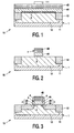
- FIGs 1 through 6 are sectional views of a semiconductor device at various stages in the manufacture of the device by means of a method in accordance with the invention.
- the device 10 (see Fig. 1 ) comprises a semiconductor body 1 which, in this case, is made of silicon but which may alternatively be made of another suitable semiconductor material.
- the basis for the body 1 is a p-type silicon substrate 11 in which an n-type so-called well 12 is formed.
- isolation regions 13 so-called trenches - of silicon dioxide are formed.
- a gate oxide 5 is formed by thermal oxidation.
- a semiconductor layer 4A here a polycrystalline silicon layer
- CVD Chemical Vapor Deposition
- a sacrificial layer 4B is deposited also by CVD, which sacrificial layer in this example is of silicon nitride, a material which may be selectively removed from the underlying polycrystalline silicon material 4A.
- a mask 111 is then formed on top of the stack at the location of the gate 4 to be formed.
- both the silicon nitride layer 4B and the polycrystalline silicon layer 4A are removed outside the area of the mask 111, by which step a gate stack 4 is formed comprising gate oxide 5, polycrystalline region 4A and sacrificial region 4B.
- the thickness of the region 4A was chosen to be 40 nm and that of the sacrificial region 4B was chosen to be 60 nm.
- the thickness of the gate stack 4 thus is approximately equal to 100 nm, which in a standard CMOS process corresponds to the height for sub 100 nm devices.
- LDD Lightly Doped Drain
- a high-energy p-type - so called HALO - tilted implantation is carried out, which is not separately shown in the drawing and which is performed to raise the channel doping at the LDD edge.
- spacers 6 are formed as follows. A dielectric layer 6 of silicon dioxide is deposited by means of CVD over the device 10. thus covering the gate stack 4. The thickness of the dielectric layer 6 in this example amounts to 90 - 100 nm.
- the deposited layer is again removed such that the surface of the body 1 at both sides of the gate stack 4 as well as the upper surface of the sacrificial region 4B are clear. Due to the isotropic nature of the etching, spacers 6 of silicon dioxide remain attached to the side faces of the gate stack 4. Now deeper n+ type implantations 2A,3A are carried out in order to complete the source and drain 2,3 formation.
- the semiconductor body is then annealed at a temperature of 1000 to 1100 degree Celsius in order to activate the source and drain implantations 2A,2B,3A,3B.
- Fig. 3 shows all these steps in a single picture.
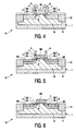
- the sacrificial region 4B of the gate stack 4 is removed by selective etching.
- Etching is done in this example by means of wet etching using hot phosphoric acid as an etchant for the silicon nitride of region 4B In this way the etching is not only selective with respect to the polycrystalline region 4A but also with respect to the silicondioxide of the spacers 6 and a thin thermal oxide which may be present on the surface of the semiconductor body 1 on both sides of the gate stack 4.
- a metal layer 7 is deposited over the structure 10.
- the metal layer 7 comprises a 10 nm thick cobalt layer and a 8 nm thick titanium layer on top thereof.
- the function of the titanium layer may be to prevent shortcuts after the silicidation and to act as a barrier for and/or getter of oxygen.
- the device 10 is thermally treated in order to form silicided regions 8, i.e. region 8A from a part of the source and drain 2,3 and region 8B from the polycrystalline region 4A.
- the formation of silicided regions 8A,8B take place by using two heating steps: a first one between 400 and 600°C, here at about 540 degrees Celsius, in which the cobalt layer 7 turns to CoSi.
- the unreacted titanium and the unreacted cobalt are removed by etching.
- a second heating step is performed between 600 and 900°C, here at about 850 degrees Celsius.
- the CoSi formed in regions 8 is converted into CoSi 2 .
- the regions 8A have a suitable thickness and on the other hand the polycrystalline region 4A becomes fully silicided region 8B.
- a depletion layer effect in the gate 4 is avoided.
- the spacers 6 are removed by dry etching.
- the resulting structure 10 now is (again) relatively planar although the height of the gate stack 4 in intermediate stages of the manufacture has been considerably larger than the resulting height of the gate 4.
- the manufacture of the MOSFET is further completed by deposition of a pre-metal dielectric, e.g. silicon dioxide, followed by patterning thereof, deposition of a contact metal layer, e.g. of aluminum, again followed by patterning. The latter steps are not shown in the Figure.
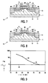
- Figs 7 and 8 are sectional views of a semiconductor device at various stages in the manufacture of the device by means of a modification of the method in accordance with the invention. Most of the steps of the method correspond to those of the previous example, and for their description reference is made here to the above part of the description. The stages shown in Figures 7 and 8 correspond to the stage of Figure 5 in the previous example.
- a thin polycrystalline silicon layer 44 is deposited by means of CVD on top of the structure 10.
- the thickness of layer 44 may be in the range of 5 to 10 nm.
- the second heating step is performed in which the CoSi is converted to CoSi 2 .
- the silicon layer 44 will be at least partly consumed in this step and the remainder thereof is removed by an etching step. In this way the requirement of an accurate determination of the polycrystalline region 4A is mitigated.
- the importance of an accurate determination of the thickness of the polycrystalline region 4A in a method without the steps of the second example can be elucidated with reference to Fig. 9 .
- Fig 9 shows the sheet resistance as a function of the thickness of the polycrystalline region of the gate of a device manufactured by a method in accordance with the invention.
- Curve 90 which connects measuring points 91 shows the sheet resistance ( ⁇ sh ) of regions 8 found in these experiments as a function of the thickness (d) of the polycrystalline region 4A of the gate 4.
- Curve 92 corresponds to the sheet resistance of bulk CoSi 2 , which is equal to about 8 ohm/square, the sheet resistance of CoSi being higher.
- silicon nitride for the sacrificial region
- other suitable materials or a combination of materials such as silicon oxynitride or an alloy of silicon and germanium.
- the spacers could (then) be made of a material other than silicondioxide, e.g. silicon nitride.
- a thermal oxide instead of a thermal oxide, a deposited oxide could be used to form the gate dielectric.
- the gate dielectric comprises silicon nitride, preferably deposited by CVD, as this material is more stable with respect to the siliciding process.
- to form a silicide other metals may be used instead of cobalt, like titanium or molybdenum.
- the silicidation could be done in a single step.
- the semiconductor body could be made of another semiconductor material such as GaAs or Germanium. In these cases still a polycrystalline or amorphous silicon gate could be used.
Landscapes
- Electrodes Of Semiconductors (AREA)
- Insulated Gate Type Field-Effect Transistor (AREA)
- Die Bonding (AREA)
Abstract
Description
- The invention relates to a method of manufacturing a semiconductor device with a field effect transistor, in which method a semiconductor body of a semiconductor material is provided, at a surface thereof, with a source region and a drain region and with a gate region between the source region and the drain region, which gate region comprises a semiconductor region of a further semiconductor material that is separated from the surface of the semiconductor body by a gate dielectric, and with spacers adjacent to the gate region for forming the source and drain regions, in which method the source region and the drain region are provided with a metal layer which is used to form a compound of the metal and the semiconductor material, and the drain region is provided with a further metal layer which is used to form a compound of the metal and the further semiconductor material. The MOSFET (= Metal Oxide Semiconductor Field Effect Transistor) with a polysilicon gate obtained by this method may suffer from the problem that a depletion layer effect therein may result in an - unwanted - reduction of the effective gate capacitance of the MOSFET and the transistor drive current. This effect has become a significant limitation in CMOS (= Complementary MOS) downscaling. Increasing the doping at the gate-gate dielectric interface can reduce said depletion layer, however gate doping is limited by the solubility of dopants in poly-silicon. Therefore alternatives to poly-silicon - or amorphous silicon or monocrystalline silicon - gates have to be found.
- A method as mentioned in the opening paragraph is known from
US patent 6,204,103 , which was issued on March 20, 2001. Therein such a method is described incolumn 6 line 51 to column 7line 10, in which the source and the drain of a silicon MOSFET are silicided with one metal layer and the gate is silicided with another metal layer, the latter metal layer being different for the polysilicon gates of a NMOS and a PMOS transistor. This procedure offers the possibility of avoiding the above-mentioned depletion effect and thus reduction of the effective gate capacitance may be avoided. - A drawback of such a method is that it is rather complicated as it comprises different steps for siliciding source and drain on the one hand and a polysilicon gate on the other hand. Moreover, it contains several other steps like a CMP (= Chemical Mechanical Polishing) step, which increase the complexity of the method.
-
US 6348390 describes a method for fabricating MOSFETs with a recessed self-aligned silicide contact and extended source/drain junctions is described. A gate structure having a gate insulating layer, a first conductive layer and a first dielectric layer is formed on a substrate. A thermal oxide layer is formed on the substrate and on sidewalls of the first conductive layer. Sidewall spacers are formed on sidewalls of the gate structure. The thermal oxide layer uncovered by the sidewall spacers is removed. The substrate is isotropically etched to form recessed regions on the substrate in regions uncovered by the gate structure and the sidewall spacers. A first metal layer is formed on the substrate after the first dielectric layer is removed. A source/drain/gate implantation is performed to the substrate, thereby forming source/drain regions under the recessed regions. -
US 2001003056 describes that after a cobalt film is deposited on a silicon-containing film formed on a semiconductor substrate, a first heat treatment at a relatively low temperature is performed with respect to the semiconductor substrate to cause a reaction between the cobalt film and the silicon layer and thereby form a Co2Si layer or CoSi layer in at least a surface portion of the silicon layer. Then, a silicon-containing film is deposited on the Co2Si layer or CoSi layer and a second heat treatment at a relatively high temperature is performed with respect to the semiconductor substrate to cause a reaction between the silicon-containing film and the Co2Si layer or CoSi layer and thereby form a CoSi2 layer in at least a surface portion of the silicon layer. - The invention is defined in the accompanying claims.
- An embodiment of the invention can avoid the above drawbacks and to provide a method which is simple and offers the possibility of avoiding the above mentioned depletion layer effect, in particular in MOSFETs with a polysilicon gate.
- In accordance with an embodiment of the invention, spacers are formed, a sacrificial region of a material that may be selectively etched with respect to the semiconductor region is deposited on top of the semiconductor region, and after the spacers have been formed, the sacrificial layer is removed by etching, and after removal of the sacrificial layer, a single metal layer is deposited contracting the source, drain and gale regions. The invention is based, inter alia, on the recognition that full silicidation of a polysilicon gate, by which the above-mentioned depletion layer effect is avoided, is possible. Moreover this may be carried out at the same time as the silicidation of the source and the drain, provided that the thickness of the polysilicon gate is limited to a thickness which is relatively small, compared to the standard gate thickness of current processes. The invention is further based on the recognition that a reduction of said thickness is unwanted as the height of a gate stack would decrease, which has large impacts on the technology used, such as on ion implant energies and spacer thickness. By providing a sacrificial region on the semiconductor region of a gate stack, the height of the gate stack may be kept constant while the layer thickness of the semiconductor region is reduced. The thickness of the sacrificial region is chosen to be complimentary to the desired reduction of the semiconductor region. Thus the above impacts on technology are avoided and at the same time the method according to the invention is relatively simple as merely a single metal layer is needed for siliciding both the source and drain regions and the gate region. The total height chosen for the gate stack depends on the technology in question, i.e. on the size of the actual transistor. As an example, for a standard CMOS process the standard semiconductor region may be e.g. 100 nm thick. In that case the semiconductor region may be reduced to e.g. 50 nm while the sacrificial region is chosen to be also 50 nm.
- The sacrificial region may be easily removed before deposition of the metal layer due to the fact that it can be etched selectively relative to e.g the polysilicon. In this way the height and width of the spacers remain unaffected as they are determined by the total height of the total gate stack. The etching of the sacrificial region may be either wet or dry.
- In summary advantages of a method according to an embodiment of the invention include that only slight changes to a standard CMOS process are required, i.e. addition of difficult steps like photolithography and CMP are not required, that it results in a fully silicide gate and thus that no depletion effect occurs during operation of the device. Moreover, the device obtained remains - after removal of the spacers - relatively planar, which makes the deposition, patterning and etching of a subsequent pre-metal dielectric layer much easier.
- In one embodiment, the spacers can be formed by depositing a layer of a dielectric material on top of the semiconductor body on which the gate region comprising the semiconductor region and the sacrificial region is present and by subsequently removing the deposited layer on top of and on both sides of the gate region by etching. This process is simple and width and height of the spacers depend on the height of the gate stack and the thickness of the dielectric layer deposited.
- From the above it is clear that the best results with respect to reduction of the depletion layer effect are obtained if the semiconductor region, e.g. the polysilicon, is completely consumed during the formation of the compound of the metal and the further semiconductor material.
- In one embodiment, the formation of the compounds between the metal and the semiconductor material and the metal and the further semiconductor material is carried out in two separate heating steps, the first heating step resulting in an intermediate compound with a lower content of the semiconductor material or the further semiconductor material and in the second heating step the intermediate compound being converted to the compound having a higher content of the semiconductor material or of the further semiconductor material. Thus, in case of a silicon MOST and a Cobalt metal layer, the intermediate compound will be e.g. CoSi while the compound will be CoSi2. The sheet resistance of the latter material is considerably smaller than that of the former, which clearly is an important advantage. In one embodiment, a part of the metal layer which has not reacted to form the intermediate compound is removed by etching between the first and the second heating step.
- In another modification, a layer of the further semiconductor material, i.e. a polysilicon layer in the case of a silicon MOST, is deposited on the surface of the semiconductor body between the two heating steps. During the second thermal treatment this layer, which is e.g. 5 to 10 nm thick, acts as a source of silicon for the formation of e.g. CoSi2 from the CoSi. Therefore, the deposition of this layer relieves constraints on the thickness of the poly-silicon consumable gate, i.e. the semiconductor silicon region of the gate. The unreacted part of e.g. the polysilicon layer is removed after the second heating step. This may be done either by a selective dry or wet etch or by oxidation and subsequent removal of the resulting oxide by an etching agent based on HF.
- The spacers can be removed after the formation of the compounds of the metal and the semiconductor material and of the metal and the further semiconductor material, In this way the resulting structure remains relatively planar. In general silicon is the preferred material for the semiconductor material and the further semiconductor material, while the intermediate compound and the compound are formed by silicides. Silicon is presently the most widely and most successfully used material within the semiconductor industry.
-
Figures 1 through 6 are sectional views of a semiconductor device at various stages in the manufacture of the device by means of a method in accordance with the invention. The device 10 (seeFig. 1 ) comprises asemiconductor body 1 which, in this case, is made of silicon but which may alternatively be made of another suitable semiconductor material. The basis for thebody 1 is a p-type silicon substrate 11 in which an n-type so-calledwell 12 is formed. In thebody 1 isolation regions 13 - so-called trenches - of silicon dioxide are formed. Subsequently on the surface of the silicon body 1 agate oxide 5 is formed by thermal oxidation. Then asemiconductor layer 4A, here a polycrystalline silicon layer, is formed by CVD (= Chemical Vapor Deposition) on top of which asacrificial layer 4B is deposited also by CVD, which sacrificial layer in this example is of silicon nitride, a material which may be selectively removed from the underlyingpolycrystalline silicon material 4A. Amask 111 is then formed on top of the stack at the location of thegate 4 to be formed. - Subsequently (see
Fig. 2 ) both thesilicon nitride layer 4B and thepolycrystalline silicon layer 4A are removed outside the area of themask 111, by which step agate stack 4 is formed comprisinggate oxide 5,polycrystalline region 4A andsacrificial region 4B. The thickness of theregion 4A was chosen to be 40 nm and that of thesacrificial region 4B was chosen to be 60 nm. The thickness of thegate stack 4 thus is approximately equal to 100 nm, which in a standard CMOS process corresponds to the height forsub 100 nm devices. - Next (see
Fig. 3 ) shallow n-type implantations drain regions spacers 6 are formed as follows. Adielectric layer 6 of silicon dioxide is deposited by means of CVD over thedevice 10. thus covering thegate stack 4. The thickness of thedielectric layer 6 in this example amounts to 90 - 100 nm. Then, by means of dry etching, the deposited layer is again removed such that the surface of thebody 1 at both sides of thegate stack 4 as well as the upper surface of thesacrificial region 4B are clear. Due to the isotropic nature of the etching,spacers 6 of silicon dioxide remain attached to the side faces of thegate stack 4. Now deepern+ type implantations drain drain implantations Fig. 3 shows all these steps in a single picture. - Subsequently (see
Fig. 4 ) thesacrificial region 4B of thegate stack 4 is removed by selective etching. Etching is done in this example by means of wet etching using hot phosphoric acid as an etchant for the silicon nitride ofregion 4B In this way the etching is not only selective with respect to thepolycrystalline region 4A but also with respect to the silicondioxide of thespacers 6 and a thin thermal oxide which may be present on the surface of thesemiconductor body 1 on both sides of thegate stack 4. Next, a metal layer 7 is deposited over thestructure 10. In this example the metal layer 7 comprises a 10 nm thick cobalt layer and a 8 nm thick titanium layer on top thereof. The function of the titanium layer may be to prevent shortcuts after the silicidation and to act as a barrier for and/or getter of oxygen. - Next (see
Fig. 5 ) thedevice 10 is thermally treated in order to form silicided regions 8, i.e.region 8A from a part of the source anddrain region 8B from thepolycrystalline region 4A. In this example the formation ofsilicided regions regions 8A have a suitable thickness and on the other hand thepolycrystalline region 4A becomes fullysilicided region 8B. Thus, a depletion layer effect in thegate 4 is avoided. - Finally (see
Fig. 6 ) thespacers 6 are removed by dry etching. The resultingstructure 10 now is (again) relatively planar although the height of thegate stack 4 in intermediate stages of the manufacture has been considerably larger than the resulting height of thegate 4. The manufacture of the MOSFET is further completed by deposition of a pre-metal dielectric, e.g. silicon dioxide, followed by patterning thereof, deposition of a contact metal layer, e.g. of aluminum, again followed by patterning. The latter steps are not shown in the Figure. -
Figs 7 and 8 are sectional views of a semiconductor device at various stages in the manufacture of the device by means of a modification of the method in accordance with the invention. Most of the steps of the method correspond to those of the previous example, and for their description reference is made here to the above part of the description. The stages shown inFigures 7 and 8 correspond to the stage ofFigure 5 in the previous example. After the first heating step (seeFigure 7 ) in which the metal layer 7 has reacted with silicon, thereby formingsilicide regions polycrystalline silicon layer 44 is deposited by means of CVD on top of thestructure 10. The thickness oflayer 44 may be in the range of 5 to 10 nm. Next (seeFig. 8 ) the second heating step is performed in which the CoSi is converted to CoSi2. Thesilicon layer 44 will be at least partly consumed in this step and the remainder thereof is removed by an etching step. In this way the requirement of an accurate determination of thepolycrystalline region 4A is mitigated. The importance of an accurate determination of the thickness of thepolycrystalline region 4A in a method without the steps of the second example can be elucidated with reference toFig. 9 . -
Fig 9 shows the sheet resistance as a function of the thickness of the polycrystalline region of the gate of a device manufactured by a method in accordance with the invention.Curve 90 which connects measuringpoints 91 shows the sheet resistance (ρsh) of regions 8 found in these experiments as a function of the thickness (d) of thepolycrystalline region 4A of thegate 4.Curve 92 corresponds to the sheet resistance of bulk CoSi2, which is equal to about 8 ohm/square, the sheet resistance of CoSi being higher. Thus, it is clear that, in this example, the conditions of which correspond to those of the first embodiment described above, only for a thickness of theregion 4A of about 40 nm, the desired full conversion to CoSi2 is realized. - It will be obvious that the invention is not limited to the examples described herein, and that within the scope of the invention many variations and modifications are possible to those skilled in the art.
- For example, instead of silicon nitride for the sacrificial region also other suitable materials or a combination of materials may be used such as silicon oxynitride or an alloy of silicon and germanium. The spacers could (then) be made of a material other than silicondioxide, e.g. silicon nitride. Furthermore, instead of a thermal oxide, a deposited oxide could be used to form the gate dielectric. In a favorable modification, the gate dielectric comprises silicon nitride, preferably deposited by CVD, as this material is more stable with respect to the siliciding process. It is further noted that to form a silicide other metals may be used instead of cobalt, like titanium or molybdenum. The silicidation could be done in a single step. The semiconductor body could be made of another semiconductor material such as GaAs or Germanium. In these cases still a polycrystalline or amorphous silicon gate could be used.
Claims (8)
- A method of manufacturing a semiconductor device (10) with a field effect transistor, in which method a semiconductor body (1) of a semiconductor material is provided, at a surface thereof, with a source region (2) and a drain region (3) and with a gate region (4) between the source region (2) and the drain region (3), which gate region comprises a semiconductor region (4A) of a further semiconductor material that is separated from the surface of the semiconductor body (1) by a gate dielectric (5), and with spacers (6) adjacent to the gate region (4) for forming the source and drain regions (2, 3), the method comprising:depositing a sacrificial region (4B) of a material on top of the semiconductor region (4A), wherein the sacrificial region (4B) is selectively etchable with respect to the semiconductor region (4A);forming the spacers (6);after the spacers (6) have been formed, removing the sacrificial layer (4B) by etching;after removal of the sacrificial layer (4B), depositing a single metal layer (7) contacting the source, drain and gate regions (2, 3, 4);forming a compound (8) of the metal and the semiconductor material of the semiconductor body (1); andforming a compound (8) of the metal and the further semiconductor material of the semiconductor region (4A) of the gate region, wherein the semiconductor region (4A) is completely consumed during the formation of the compound (8).
- A method as claimed in claim 1, wherein the spacers (6) are formed by depositing a layer of a dielectric material on top of the semiconductor body (1) on which the gate region (4) comprising the semiconductor region (4A) and the sacrificial region (4B) is present and by subsequently removing the deposited layer on top of and on both sides of the gate region (4) by etching.
- A method as claimed in claim 1 or claim 2, wherein the formation of the compounds (8) between the metal and the semiconductor material and the metal and the further semiconductor material is carried out in two separate heating steps, the first heating step resulting in an intermediate compound with a low content of the semiconductor material or of the further semiconductor material and in the second heating step the intermediate compound being converted to the compound having a higher content of the semiconductor material or of the further semiconductor material.
- A method as claimed in claim 3, wherein between the two heating steps, a part of the metal layer (7) which has not reacted to form the intermediate compound is removed by etching.
- A method as claimed in claim 3 or 4, wherein between the two heating steps, a layer (44) of the further semiconductor material is deposited on the surface of the semiconductor body (1).
- A method as claimed in claim 5, wherein after the second heating step, a part of the layer (44) of the further semiconductor material which has not reacted to form the compound is removed by etching.
- A method as claimed in anyone of the preceding claims, wherein after the formation of the compounds of the metal and the semiconductor material and of the metal and the further semiconductor material, the spacers (6) are removed.
- A method as claimed in anyone of the preceding claims, wherein for the semiconductor material as well as for the further semiconductor material silicon is chosen, and for the intermediate compound and for the compound of the metal and the semiconductor material and the further semiconductor material a metal silicide is chosen.
Priority Applications (1)
| Application Number | Priority Date | Filing Date | Title |
|---|---|---|---|
| EP20030813688 EP1579488B1 (en) | 2002-12-20 | 2003-12-15 | Method of manufacturing a semiconductor device |
Applications Claiming Priority (4)
| Application Number | Priority Date | Filing Date | Title |
|---|---|---|---|
| EP02080508 | 2002-12-20 | ||
| EP02080508 | 2002-12-20 | ||
| EP20030813688 EP1579488B1 (en) | 2002-12-20 | 2003-12-15 | Method of manufacturing a semiconductor device |
| PCT/IB2003/006009 WO2004057659A1 (en) | 2002-12-20 | 2003-12-15 | Method of manufacturing a semiconductor device and semiconductor device obtained with such a method |
Publications (2)
| Publication Number | Publication Date |
|---|---|
| EP1579488A1 EP1579488A1 (en) | 2005-09-28 |
| EP1579488B1 true EP1579488B1 (en) | 2011-12-07 |
Family
ID=32668807
Family Applications (1)
| Application Number | Title | Priority Date | Filing Date |
|---|---|---|---|
| EP20030813688 Expired - Lifetime EP1579488B1 (en) | 2002-12-20 | 2003-12-15 | Method of manufacturing a semiconductor device |
Country Status (8)
| Country | Link |
|---|---|
| US (1) | US20060152086A1 (en) |
| EP (1) | EP1579488B1 (en) |
| JP (1) | JP2006511083A (en) |
| KR (1) | KR20050084382A (en) |
| CN (1) | CN100390939C (en) |
| AT (1) | ATE536634T1 (en) |
| AU (1) | AU2003303273A1 (en) |
| WO (1) | WO2004057659A1 (en) |
Families Citing this family (14)
| Publication number | Priority date | Publication date | Assignee | Title |
|---|---|---|---|---|
| KR100481185B1 (en) | 2003-07-10 | 2005-04-07 | 삼성전자주식회사 | Method of fabricating a MOS transistor using a total gate silicidation process |
| US7235472B2 (en) | 2004-11-12 | 2007-06-26 | Infineon Technologies Ag | Method of making fully silicided gate electrode |
| JP4473741B2 (en) * | 2005-01-27 | 2010-06-02 | 株式会社東芝 | Semiconductor device and manufacturing method of semiconductor device |
| US7399702B2 (en) * | 2005-02-01 | 2008-07-15 | Infineon Technologies Ag | Methods of forming silicide |
| US7183169B1 (en) * | 2005-03-07 | 2007-02-27 | Advanced Micro Devices, Inc. | Method and arrangement for reducing source/drain resistance with epitaxial growth |
| US7737019B1 (en) * | 2005-03-08 | 2010-06-15 | Spansion Llc | Method for containing a silicided gate within a sidewall spacer in integrated circuit technology |
| US7544553B2 (en) | 2005-03-30 | 2009-06-09 | Infineon Technologies Ag | Integration scheme for fully silicided gate |
| EP1744351A3 (en) * | 2005-07-11 | 2008-11-26 | Interuniversitair Microelektronica Centrum ( Imec) | Method for forming a fully silicided gate MOSFET and devices obtained thereof |
| JP2007027727A (en) * | 2005-07-11 | 2007-02-01 | Interuniv Micro Electronica Centrum Vzw | Method for forming fully silicided gate MOSFET and device obtained by the method |
| US7723176B2 (en) * | 2005-09-01 | 2010-05-25 | Nec Corporation | Method for manufacturing semiconductor device |
| US7297618B1 (en) * | 2006-07-28 | 2007-11-20 | International Business Machines Corporation | Fully silicided gate electrodes and method of making the same |
| KR20140131671A (en) * | 2013-05-06 | 2014-11-14 | 에스케이하이닉스 주식회사 | Variable resistance device having parallel structure |
| CN105244276B (en) * | 2014-06-12 | 2018-08-21 | 中芯国际集成电路制造(上海)有限公司 | A kind of FinFET and its manufacturing method, electronic device |
| CN113690134A (en) * | 2020-05-19 | 2021-11-23 | 中国科学院微电子研究所 | Preparation method of metal silicide, semiconductor device and electronic equipment |
Family Cites Families (25)
| Publication number | Priority date | Publication date | Assignee | Title |
|---|---|---|---|---|
| KR920002350B1 (en) * | 1987-05-21 | 1992-03-21 | 마쯔시다덴기산교 가부시기가이샤 | Method of manufacturing semiconductor |
| US5352631A (en) * | 1992-12-16 | 1994-10-04 | Motorola, Inc. | Method for forming a transistor having silicided regions |
| JP2848757B2 (en) * | 1993-03-19 | 1999-01-20 | シャープ株式会社 | Field effect transistor and method of manufacturing the same |
| JPH07135317A (en) * | 1993-04-22 | 1995-05-23 | Texas Instr Inc <Ti> | Self-aligned silicide gate |
| KR100206878B1 (en) * | 1995-12-29 | 1999-07-01 | 구본준 | Semiconductor device manufacturing method |
| US5753557A (en) * | 1996-10-07 | 1998-05-19 | Vanguard International Semiconductor Company | Bridge-free self aligned silicide process |
| JP3827839B2 (en) * | 1997-11-27 | 2006-09-27 | 富士通株式会社 | Manufacturing method of semiconductor device |
| TW418448B (en) * | 1998-02-03 | 2001-01-11 | United Microelectronics Corp | A method of preventing side metal silicide growth to avoid short-circuit device and its gate structure |
| US6348390B1 (en) * | 1998-02-19 | 2002-02-19 | Acer Semiconductor Manufacturing Corp. | Method for fabricating MOSFETS with a recessed self-aligned silicide contact and extended source/drain junctions |
| US6074922A (en) * | 1998-03-13 | 2000-06-13 | Taiwan Semiconductor Manufacturing Company | Enhanced structure for salicide MOSFET |
| US6284612B1 (en) * | 1998-03-25 | 2001-09-04 | Texas Instruments - Acer Incorporated | Process to fabricate ultra-short channel MOSFETs with self-aligned silicide contact |
| US6069044A (en) * | 1998-03-30 | 2000-05-30 | Texas Instruments-Acer Incorporated | Process to fabricate ultra-short channel nMOSFETS with self-aligned silicide contact |
| JPH11284179A (en) * | 1998-03-30 | 1999-10-15 | Sony Corp | Semiconductor device and manufacturing method thereof |
| US6204103B1 (en) * | 1998-09-18 | 2001-03-20 | Intel Corporation | Process to make complementary silicide metal gates for CMOS technology |
| US6211000B1 (en) * | 1999-01-04 | 2001-04-03 | Advanced Micro Devices | Method of making high performance mosfets having high conductivity gate conductors |
| JP2000252462A (en) * | 1999-03-01 | 2000-09-14 | Toshiba Corp | MIS type semiconductor device and method of manufacturing the same |
| US6271133B1 (en) * | 1999-04-12 | 2001-08-07 | Chartered Semiconductor Manufacturing Ltd. | Optimized Co/Ti-salicide scheme for shallow junction deep sub-micron device fabrication |
| JP3554514B2 (en) * | 1999-12-03 | 2004-08-18 | 松下電器産業株式会社 | Semiconductor device and manufacturing method thereof |
| JP2001189284A (en) * | 1999-12-27 | 2001-07-10 | Mitsubishi Electric Corp | Semiconductor device and method of manufacturing the same |
| US6620718B1 (en) * | 2000-04-25 | 2003-09-16 | Advanced Micro Devices, Inc. | Method of forming metal silicide regions on a gate electrode and on the source/drain regions of a semiconductor device |
| US6423634B1 (en) * | 2000-04-25 | 2002-07-23 | Advanced Micro Devices, Inc. | Method of forming low resistance metal silicide region on a gate electrode of a transistor |
| US20020031909A1 (en) * | 2000-05-11 | 2002-03-14 | Cyril Cabral | Self-aligned silicone process for low resistivity contacts to thin film silicon-on-insulator mosfets |
| US6365468B1 (en) * | 2000-06-21 | 2002-04-02 | United Microelectronics Corp. | Method for forming doped p-type gate with anti-reflection layer |
| DE10033367C2 (en) * | 2000-07-08 | 2002-04-25 | Porsche Ag | Internal combustion engine, in particular for motorcycles |
| US7067379B2 (en) * | 2004-01-08 | 2006-06-27 | Taiwan Semiconductor Manufacturing Company, Ltd. | Silicide gate transistors and method of manufacture |
-
2003
- 2003-12-15 WO PCT/IB2003/006009 patent/WO2004057659A1/en not_active Ceased
- 2003-12-15 EP EP20030813688 patent/EP1579488B1/en not_active Expired - Lifetime
- 2003-12-15 US US10/539,224 patent/US20060152086A1/en not_active Abandoned
- 2003-12-15 CN CNB2003801064123A patent/CN100390939C/en not_active Expired - Fee Related
- 2003-12-15 JP JP2004561869A patent/JP2006511083A/en active Pending
- 2003-12-15 AU AU2003303273A patent/AU2003303273A1/en not_active Abandoned
- 2003-12-15 KR KR1020057011201A patent/KR20050084382A/en not_active Ceased
- 2003-12-15 AT AT03813688T patent/ATE536634T1/en active
Also Published As
| Publication number | Publication date |
|---|---|
| CN100390939C (en) | 2008-05-28 |
| JP2006511083A (en) | 2006-03-30 |
| EP1579488A1 (en) | 2005-09-28 |
| KR20050084382A (en) | 2005-08-26 |
| AU2003303273A1 (en) | 2004-07-14 |
| US20060152086A1 (en) | 2006-07-13 |
| CN1726582A (en) | 2006-01-25 |
| ATE536634T1 (en) | 2011-12-15 |
| WO2004057659A1 (en) | 2004-07-08 |
Similar Documents
| Publication | Publication Date | Title |
|---|---|---|
| US5352631A (en) | Method for forming a transistor having silicided regions | |
| US5496750A (en) | Elevated source/drain junction metal oxide semiconductor field-effect transistor using blanket silicon deposition | |
| US7211515B2 (en) | Methods of forming silicide layers on source/drain regions of MOS transistors | |
| US6908850B2 (en) | Structure and method for silicided metal gate transistors | |
| US7397091B2 (en) | SiGe nickel barrier structure employed in a CMOS device to prevent excess diffusion of nickel used in the silicide material | |
| CN103000675B (en) | Low source-drain contact resistance MOSFETS and manufacturing method thereof | |
| US6806534B2 (en) | Damascene method for improved MOS transistor | |
| US7723762B2 (en) | Schottky barrier FinFET device and fabrication method thereof | |
| US5851891A (en) | IGFET method of forming with silicide contact on ultra-thin gate | |
| CN100576473C (en) | Method for manufacturing semiconductor device having silicided gate electrode and method for manufacturing integrated circuit including same | |
| EP1579488B1 (en) | Method of manufacturing a semiconductor device | |
| US6784506B2 (en) | Silicide process using high K-dielectrics | |
| US7545006B2 (en) | CMOS devices with graded silicide regions | |
| CN101488453A (en) | Structure and method to fabricate MOSFET with short gate | |
| JPH11284179A (en) | Semiconductor device and manufacturing method thereof | |
| US6326291B1 (en) | Fabrication of a wide metal silicide on a narrow polysilicon gate structure | |
| US7078347B2 (en) | Method for forming MOS transistors with improved sidewall structures | |
| US7544553B2 (en) | Integration scheme for fully silicided gate | |
| JP4152265B2 (en) | Manufacturing method of semiconductor device | |
| US20250015161A1 (en) | Semiconductor device and fabrication method thereof | |
| US20080286931A1 (en) | Semiconductor device including field-effect transistor using salicide (self-aligned silicide) structure and method of fabricating the same | |
| JP4602138B2 (en) | Manufacturing method of semiconductor device | |
| US20080054380A1 (en) | Semiconductor Device and Method for Manufacturing the Same | |
| KR100628214B1 (en) | Manufacturing method of semiconductor device | |
| KR100850096B1 (en) | Method for manufacturing mos transistor |
Legal Events
| Date | Code | Title | Description |
|---|---|---|---|
| PUAI | Public reference made under article 153(3) epc to a published international application that has entered the european phase |
Free format text: ORIGINAL CODE: 0009012 |
|
| 17P | Request for examination filed |
Effective date: 20050720 |
|
| AK | Designated contracting states |
Kind code of ref document: A1 Designated state(s): AT BE BG CH CY CZ DE DK EE ES FI FR GB GR HU IE IT LI LU MC NL PT RO SE SI SK TR |
|
| AX | Request for extension of the european patent |
Extension state: AL LT LV MK |
|
| DAX | Request for extension of the european patent (deleted) | ||
| RAP1 | Party data changed (applicant data changed or rights of an application transferred) |
Owner name: INTERUNIVERSITAIR MICROELEKTRONICA CENTRUM VZW Owner name: NXP B.V. |
|
| 17Q | First examination report despatched |
Effective date: 20090518 |
|
| RAP1 | Party data changed (applicant data changed or rights of an application transferred) |
Owner name: IMEC Owner name: NXP B.V. |
|
| GRAP | Despatch of communication of intention to grant a patent |
Free format text: ORIGINAL CODE: EPIDOSNIGR1 |
|
| RTI1 | Title (correction) |
Free format text: METHOD OF MANUFACTURING A SEMICONDUCTOR DEVICE |
|
| GRAS | Grant fee paid |
Free format text: ORIGINAL CODE: EPIDOSNIGR3 |
|
| GRAA | (expected) grant |
Free format text: ORIGINAL CODE: 0009210 |
|
| AK | Designated contracting states |
Kind code of ref document: B1 Designated state(s): AT BE BG CH CY CZ DE DK EE ES FI FR GB GR HU IE IT LI LU MC NL PT RO SE SI SK TR |
|
| REG | Reference to a national code |
Ref country code: GB Ref legal event code: FG4D |
|
| REG | Reference to a national code |
Ref country code: CH Ref legal event code: EP |
|
| REG | Reference to a national code |
Ref country code: IE Ref legal event code: FG4D |
|
| REG | Reference to a national code |
Ref country code: DE Ref legal event code: R096 Ref document number: 60339359 Country of ref document: DE Effective date: 20120126 |
|
| REG | Reference to a national code |
Ref country code: NL Ref legal event code: VDEP Effective date: 20111207 |
|
| PGFP | Annual fee paid to national office [announced via postgrant information from national office to epo] |
Ref country code: FR Payment date: 20120119 Year of fee payment: 9 |
|
| PG25 | Lapsed in a contracting state [announced via postgrant information from national office to epo] |
Ref country code: NL Free format text: LAPSE BECAUSE OF FAILURE TO SUBMIT A TRANSLATION OF THE DESCRIPTION OR TO PAY THE FEE WITHIN THE PRESCRIBED TIME-LIMIT Effective date: 20111207 Ref country code: SI Free format text: LAPSE BECAUSE OF FAILURE TO SUBMIT A TRANSLATION OF THE DESCRIPTION OR TO PAY THE FEE WITHIN THE PRESCRIBED TIME-LIMIT Effective date: 20111207 Ref country code: SE Free format text: LAPSE BECAUSE OF FAILURE TO SUBMIT A TRANSLATION OF THE DESCRIPTION OR TO PAY THE FEE WITHIN THE PRESCRIBED TIME-LIMIT Effective date: 20111207 Ref country code: GR Free format text: LAPSE BECAUSE OF FAILURE TO SUBMIT A TRANSLATION OF THE DESCRIPTION OR TO PAY THE FEE WITHIN THE PRESCRIBED TIME-LIMIT Effective date: 20120308 |
|
| PG25 | Lapsed in a contracting state [announced via postgrant information from national office to epo] |
Ref country code: CY Free format text: LAPSE BECAUSE OF FAILURE TO SUBMIT A TRANSLATION OF THE DESCRIPTION OR TO PAY THE FEE WITHIN THE PRESCRIBED TIME-LIMIT Effective date: 20111207 Ref country code: BE Free format text: LAPSE BECAUSE OF FAILURE TO SUBMIT A TRANSLATION OF THE DESCRIPTION OR TO PAY THE FEE WITHIN THE PRESCRIBED TIME-LIMIT Effective date: 20111207 |
|
| PGFP | Annual fee paid to national office [announced via postgrant information from national office to epo] |
Ref country code: GB Payment date: 20120131 Year of fee payment: 9 |
|
| PG25 | Lapsed in a contracting state [announced via postgrant information from national office to epo] |
Ref country code: EE Free format text: LAPSE BECAUSE OF FAILURE TO SUBMIT A TRANSLATION OF THE DESCRIPTION OR TO PAY THE FEE WITHIN THE PRESCRIBED TIME-LIMIT Effective date: 20111207 Ref country code: BG Free format text: LAPSE BECAUSE OF FAILURE TO SUBMIT A TRANSLATION OF THE DESCRIPTION OR TO PAY THE FEE WITHIN THE PRESCRIBED TIME-LIMIT Effective date: 20120307 Ref country code: SK Free format text: LAPSE BECAUSE OF FAILURE TO SUBMIT A TRANSLATION OF THE DESCRIPTION OR TO PAY THE FEE WITHIN THE PRESCRIBED TIME-LIMIT Effective date: 20111207 Ref country code: MC Free format text: LAPSE BECAUSE OF NON-PAYMENT OF DUE FEES Effective date: 20111231 Ref country code: CZ Free format text: LAPSE BECAUSE OF FAILURE TO SUBMIT A TRANSLATION OF THE DESCRIPTION OR TO PAY THE FEE WITHIN THE PRESCRIBED TIME-LIMIT Effective date: 20111207 |
|
| PGFP | Annual fee paid to national office [announced via postgrant information from national office to epo] |
Ref country code: DE Payment date: 20120123 Year of fee payment: 9 |
|
| REG | Reference to a national code |
Ref country code: CH Ref legal event code: PL |
|
| PG25 | Lapsed in a contracting state [announced via postgrant information from national office to epo] |
Ref country code: RO Free format text: LAPSE BECAUSE OF FAILURE TO SUBMIT A TRANSLATION OF THE DESCRIPTION OR TO PAY THE FEE WITHIN THE PRESCRIBED TIME-LIMIT Effective date: 20111207 Ref country code: PT Free format text: LAPSE BECAUSE OF FAILURE TO SUBMIT A TRANSLATION OF THE DESCRIPTION OR TO PAY THE FEE WITHIN THE PRESCRIBED TIME-LIMIT Effective date: 20120409 |
|
| REG | Reference to a national code |
Ref country code: AT Ref legal event code: MK05 Ref document number: 536634 Country of ref document: AT Kind code of ref document: T Effective date: 20111207 |
|
| REG | Reference to a national code |
Ref country code: IE Ref legal event code: MM4A |
|
| PLBE | No opposition filed within time limit |
Free format text: ORIGINAL CODE: 0009261 |
|
| STAA | Information on the status of an ep patent application or granted ep patent |
Free format text: STATUS: NO OPPOSITION FILED WITHIN TIME LIMIT |
|
| PG25 | Lapsed in a contracting state [announced via postgrant information from national office to epo] |
Ref country code: IE Free format text: LAPSE BECAUSE OF NON-PAYMENT OF DUE FEES Effective date: 20111215 Ref country code: DK Free format text: LAPSE BECAUSE OF FAILURE TO SUBMIT A TRANSLATION OF THE DESCRIPTION OR TO PAY THE FEE WITHIN THE PRESCRIBED TIME-LIMIT Effective date: 20111207 Ref country code: CH Free format text: LAPSE BECAUSE OF NON-PAYMENT OF DUE FEES Effective date: 20111231 Ref country code: LI Free format text: LAPSE BECAUSE OF NON-PAYMENT OF DUE FEES Effective date: 20111231 |
|
| 26N | No opposition filed |
Effective date: 20120910 |
|
| PG25 | Lapsed in a contracting state [announced via postgrant information from national office to epo] |
Ref country code: IT Free format text: LAPSE BECAUSE OF FAILURE TO SUBMIT A TRANSLATION OF THE DESCRIPTION OR TO PAY THE FEE WITHIN THE PRESCRIBED TIME-LIMIT Effective date: 20111207 |
|
| REG | Reference to a national code |
Ref country code: DE Ref legal event code: R097 Ref document number: 60339359 Country of ref document: DE Effective date: 20120910 |
|
| PG25 | Lapsed in a contracting state [announced via postgrant information from national office to epo] |
Ref country code: AT Free format text: LAPSE BECAUSE OF FAILURE TO SUBMIT A TRANSLATION OF THE DESCRIPTION OR TO PAY THE FEE WITHIN THE PRESCRIBED TIME-LIMIT Effective date: 20111207 |
|
| PG25 | Lapsed in a contracting state [announced via postgrant information from national office to epo] |
Ref country code: ES Free format text: LAPSE BECAUSE OF FAILURE TO SUBMIT A TRANSLATION OF THE DESCRIPTION OR TO PAY THE FEE WITHIN THE PRESCRIBED TIME-LIMIT Effective date: 20120318 |
|
| PG25 | Lapsed in a contracting state [announced via postgrant information from national office to epo] |
Ref country code: LU Free format text: LAPSE BECAUSE OF NON-PAYMENT OF DUE FEES Effective date: 20111215 |
|
| PG25 | Lapsed in a contracting state [announced via postgrant information from national office to epo] |
Ref country code: FI Free format text: LAPSE BECAUSE OF FAILURE TO SUBMIT A TRANSLATION OF THE DESCRIPTION OR TO PAY THE FEE WITHIN THE PRESCRIBED TIME-LIMIT Effective date: 20111207 |
|
| GBPC | Gb: european patent ceased through non-payment of renewal fee |
Effective date: 20121215 |
|
| REG | Reference to a national code |
Ref country code: FR Ref legal event code: ST Effective date: 20130830 |
|
| PG25 | Lapsed in a contracting state [announced via postgrant information from national office to epo] |
Ref country code: TR Free format text: LAPSE BECAUSE OF FAILURE TO SUBMIT A TRANSLATION OF THE DESCRIPTION OR TO PAY THE FEE WITHIN THE PRESCRIBED TIME-LIMIT Effective date: 20111207 |
|
| REG | Reference to a national code |
Ref country code: DE Ref legal event code: R119 Ref document number: 60339359 Country of ref document: DE Effective date: 20130702 |
|
| PG25 | Lapsed in a contracting state [announced via postgrant information from national office to epo] |
Ref country code: HU Free format text: LAPSE BECAUSE OF FAILURE TO SUBMIT A TRANSLATION OF THE DESCRIPTION OR TO PAY THE FEE WITHIN THE PRESCRIBED TIME-LIMIT Effective date: 20111207 Ref country code: DE Free format text: LAPSE BECAUSE OF NON-PAYMENT OF DUE FEES Effective date: 20130702 |
|
| PG25 | Lapsed in a contracting state [announced via postgrant information from national office to epo] |
Ref country code: GB Free format text: LAPSE BECAUSE OF NON-PAYMENT OF DUE FEES Effective date: 20121215 Ref country code: FR Free format text: LAPSE BECAUSE OF NON-PAYMENT OF DUE FEES Effective date: 20130102 |