EP1577941A2 - Method for creating a pattern in a material and semiconductor structure processed therewith - Google Patents
Method for creating a pattern in a material and semiconductor structure processed therewith Download PDFInfo
- Publication number
- EP1577941A2 EP1577941A2 EP05003847A EP05003847A EP1577941A2 EP 1577941 A2 EP1577941 A2 EP 1577941A2 EP 05003847 A EP05003847 A EP 05003847A EP 05003847 A EP05003847 A EP 05003847A EP 1577941 A2 EP1577941 A2 EP 1577941A2
- Authority
- EP
- European Patent Office
- Prior art keywords
- pattern
- mask layer
- layer
- accordance
- mask
- Prior art date
- Legal status (The legal status is an assumption and is not a legal conclusion. Google has not performed a legal analysis and makes no representation as to the accuracy of the status listed.)
- Granted
Links
Images


Classifications
-
- H—ELECTRICITY
- H10—SEMICONDUCTOR DEVICES; ELECTRIC SOLID-STATE DEVICES NOT OTHERWISE PROVIDED FOR
- H10P—GENERIC PROCESSES OR APPARATUS FOR THE MANUFACTURE OR TREATMENT OF DEVICES COVERED BY CLASS H10
- H10P76/00—Manufacture or treatment of masks on semiconductor bodies, e.g. by lithography or photolithography
- H10P76/40—Manufacture or treatment of masks on semiconductor bodies, e.g. by lithography or photolithography of masks comprising inorganic materials
- H10P76/408—Manufacture or treatment of masks on semiconductor bodies, e.g. by lithography or photolithography of masks comprising inorganic materials characterised by their sizes, orientations, dispositions, behaviours or shapes
- H10P76/4088—Processes for improving the resolution of the masks
-
- H—ELECTRICITY
- H10—SEMICONDUCTOR DEVICES; ELECTRIC SOLID-STATE DEVICES NOT OTHERWISE PROVIDED FOR
- H10P—GENERIC PROCESSES OR APPARATUS FOR THE MANUFACTURE OR TREATMENT OF DEVICES COVERED BY CLASS H10
- H10P50/00—Etching of wafers, substrates or parts of devices
- H10P50/73—Etching of wafers, substrates or parts of devices using masks for insulating materials
-
- H—ELECTRICITY
- H10—SEMICONDUCTOR DEVICES; ELECTRIC SOLID-STATE DEVICES NOT OTHERWISE PROVIDED FOR
- H10P—GENERIC PROCESSES OR APPARATUS FOR THE MANUFACTURE OR TREATMENT OF DEVICES COVERED BY CLASS H10
- H10P76/00—Manufacture or treatment of masks on semiconductor bodies, e.g. by lithography or photolithography
- H10P76/40—Manufacture or treatment of masks on semiconductor bodies, e.g. by lithography or photolithography of masks comprising inorganic materials
- H10P76/408—Manufacture or treatment of masks on semiconductor bodies, e.g. by lithography or photolithography of masks comprising inorganic materials characterised by their sizes, orientations, dispositions, behaviours or shapes
- H10P76/4085—Manufacture or treatment of masks on semiconductor bodies, e.g. by lithography or photolithography of masks comprising inorganic materials characterised by their sizes, orientations, dispositions, behaviours or shapes characterised by the processes involved to create the masks
-
- H—ELECTRICITY
- H10—SEMICONDUCTOR DEVICES; ELECTRIC SOLID-STATE DEVICES NOT OTHERWISE PROVIDED FOR
- H10W—GENERIC PACKAGES, INTERCONNECTIONS, CONNECTORS OR OTHER CONSTRUCTIONAL DETAILS OF DEVICES COVERED BY CLASS H10
- H10W20/00—Interconnections in chips, wafers or substrates
- H10W20/01—Manufacture or treatment
- H10W20/071—Manufacture or treatment of dielectric parts thereof
- H10W20/081—Manufacture or treatment of dielectric parts thereof by forming openings in the dielectric parts
- H10W20/089—Manufacture or treatment of dielectric parts thereof by forming openings in the dielectric parts using processes for implementing desired shapes or dispositions of the openings, e.g. double patterning
Definitions
- the invention relates to a method of manufacturing a semiconductor device wherein a pattern is created in a material, the method comprising covering the material with a lower mask layer and covering the lower mask layer with an upper mask layer, creating a first pattern on the upper mask layer by means of a lithographic mask and removing a part of the upper mask layer in dependency on the first pattern. Further, the invention relates to a semiconductor structure processed with the method according to the invention.
- Patent Abstracts of Japan, 2000-223490 describes the manufacture of a semiconductor device. On a silicon oxide film, an organic layer is formed. The organic layer is then covered by two stacked inorganic masks, such that the lower inorganic mask protects the organic layer while removing resist.
- a problem associated with the prior art is that dimensions in microcircuits, such as integrated circuits, are becoming smaller and smaller. Dimensions of patterns defined in such materials, or other materials, are however limited by a resolution of an imaging system for applying the pattern on the material. Thus, dimensions of structures such as trenches and IMD are limited by a resolution of the imaging system.
- a goal of the invention is to enable providing structures having smaller dimensions.
- the method according to the invention is characterized by creating, by means of the lithographic mask, a second pattern on the upper mask layer or on the lower mask layer at locations where the upper mask layer has been removed, the mask being displaced over a distance such that the second pattern is displaced with respect to the first pattern, and removing a part of the lower mask layer and/or the upper mask layer in accordance with at least the second pattern and removing a part of the material in accordance with a mask formed by remaining parts of the lower and the upper mask layers.
- the upper mask layer is patterned in accordance with the lithographical mask. Then, the mask is displaced over a distance, and a second pattern is created which is thus identical to the first pattern but displaced over said distance with respect to the first pattern.
- the second pattern is provided on the upper mask layer or on the lower mask layer at the locations where the upper mask layer has been removed in dependency on the first pattern.
- a part of the lower mask layer and/or the upper mask layer is removed.
- a mask is created by the remaining parts of the lower mask layer and the upper mask layer.
- a resolution of this resulting mask is exclusively determined by the resolution of the imaging system which projects the lithographic mask on the respective layer.
- the step of removing a part of the lower mask layer and/or the upper mask layer in accordance with at least the second pattern comprises removing a part of the lower mask layer in accordance with the second pattern overlaid with a pattern formed by a remaining part of the upper mask layer.
- the remaining part of the upper mask layer after removal of a part of the upper mask layer in dependency on the first pattern.
- a part of the underlying material can be removed with the resulting mask formed by the remaining parts of the lower and the upper mask layers. Due to the removal of the smaller part of the lower mask layer, small structures, such as small trenches or other openings can be created in the material.
- the step of removing a part of the lower mask layer and/or the upper mask layer in accordance with at least the second pattern comprises removing a part of the upper mask layer in accordance with the second pattern, and removing a part of the lower mask layer in accordance with a pattern formed by the upper mask layer.
- the removal of a part of any of the mask layers, i.e. the lower mask layer and/or the upper mask layer, is performed by selective etching of the respective layer in accordance with the respective pattern.
- the respective layer i.e. the upper mask layer or the lower mask layer is etched, and not the other one of the mask layers.
- the material can comprise an organic and/or an inorganic material.
- inorganic materials such as inorganic dielectric materials
- the material comprises a layer of organic material covering a layer of inorganic material.
- the removal of a part of the material in accordance with a mask formed by the remaining parts of the lower and the upper mask layers comprises removing a part of the organic material in accordance with the mask formed by remaining parts of the lower and the upper mask layers, removing a part of the inorganic material in accordance with the mask formed by a remaining part of at least the organic material, and removing the remaining part of the organic material.
- the organic material is patterned in accordance with the steps as described above, and then a part of the inorganic material is removed using the remaining part of the organic material as a mask, and the remaining part of the organic material can be removed, after which the desired pattern in the organic material results.
- the method advantageously comprises the further step of removing the remaining parts of the lower and the upper mask layers.
- the layers can be removed by any suitable removal technique, such as wet or dry etching, chemical mechanical polishing.
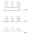
- Figs. 1a-1d show a cross-sectional view of a (part of a) semiconductor structure comprising an inorganic dielectric 1 formed upon a substrate 7.
- This substrate can be a conductive or semiconductive substrate such as silicon, germanium, silicon-on-insulator. It can be a non-conductive substrate such as a ceramic plate, a quartz plate, a thin film substrate.
- On top of the inorganic dielectric a layer of organic material 2 is provided.
- the layer of organic material 2 in turn is covered by a lower mask layer, indicated in the Figures as hard mask 2 (inorganic), which in turn is covered by an upper mask layer, indicated in the Figures as hard mask 1 (inorganic).
- the inorganic material is the layer that needs to be patterned and the other layers shown are sacrificial layers used in the process.
- a layer of resist 5 is applied and, as shown in Fig. 1b, a pattern is transferred into the resist 5, e.g. by means of a standard lithography step.
- the pattern is now etched into the upper mask layer 4 by using an etch recipe that is selective towards the lower mask layer, i.e. only etches the upper mask layer 4 and does not etch the lower mask layer 3.
- the resist 5 is stripped, the result of which is shown in Fig. 1c.
- a new layer of resist 6 is provided on top of the structure and the pattern is again transferred into the resist 6, and the applicable portions of the resist 6 are removed in dependency on the pattern, in a way similar to the pattern as shown with reference to Fig. 1b, however the second pattern as shown with reference to Fig. 1d is displaced over a distance with respect to the earlier (i.e. the first) pattern as shown with reference to Fig. 1b.
- the pattern in the resist 6 in Fig. 1d creates a pattern on the upper mask layer 4, where present, and on the lower mask layer 3 at locations where the upper mask layer 4 has been removed.
- the further steps for the creation of a small trench are shown with reference to Figs. 2a-2d, while the further steps for the creation of a small spacing are shown with reference to Figs. 3a-3d.
- the further steps comprise the removal of a part of the lower mask layer and/or the upper mask layer in accordance with at least the second pattern, and the removal of a part of the material, i.e. the organic or inorganic layer, in accordance with a mask formed by remaining parts of the lower and upper mask layers.
- the part of the lower mask layer 3 is etched with an etch recipe that is selective towards the upper mask layer 4, and thus does not affect the organic material 2 or the upper mask layer 4.
- small trenches are created in the lower mask layer 3, the trenches being indicated by 3a.
- the small trenches 3a in the lower mask layer 3 have a width that consists only of the overlapping exposed parts of the first pattern and the second pattern.
- the dimension (in this example the width) of the trench 3a is reduced as compared to the width of the opening in the first pattern, such as e.g. in the resist 5 and the upper mask layer 4, or in the second pattern, such as e.g.
- the organic material 2 is etched thereby also removing the resist 6. Due to the small dimensions of the trench 3a in the lower mask layer 3, the trenches in the organic material 2 will also have the same or substantially the same small dimension.
- the pattern as present in the organic material 2 is etched into the inorganic dielectric 1, and subsequently the two hard masks 3, 4 are removed. Finally, also the organic material 2 will be removed, as shown in Fig. 2d.
- Figs. 3a-3f further steps for creating a small spacing will be shown with reference to Figs. 3a-3f.
- the upper mask layer 4 is again selectively etched with the second pattern as formed in the resist 6.
- the resist 6 is removed, e.g. stripped afterwards, as shown in Fig. 3b.
- a spacing 4a is created, of which the dimension is smaller than the dimension obtainable with the resolution of the first pattern and the second pattern.
- the selective etching of the upper mask layer 4 is to be interpreted as an etching operation which (substantially) does not affect the lower mask layer 3, and vice versa.
- the lower mask layer 3 is etched selectively, without affecting the upper mask layer 4, the result of which is shown in Fig. 3c.
- the spacing 4a now defined in the upper mask layer 4 and the lower mask layer 3 consists only of the overlapping parts of the two patterns.
- the dimensions of the spacing 4a are reduced as compared to the spacing of the first and second pattern.
- the pattern in the lower mask layer 3 and/or upper mask layer 4 is used as a mask to etch the organic layer 2, the result of which is shown in Fig. 3d.
- the pattern now present in the organic layer 2 is used as a mask for the inorganic layer 1 when etching the inorganic layer 1.
- the lower mask layer 3 and upper mask layer 4 are etched, the result of which is shown in Fig. 3e.
- the inorganic material 2 is removed, for example stripped.
- a displacement of the second pattern with regard to the first pattern is a one-dimensional displacement
- the mask can also be displaced such that the second pattern is displaced in two dimensions in a plane of the layer of materials.
- structures having a small dimension can be achieved in two dimensions in the plane of the material layers with one sequence of process steps as described with reference to Fig. 1 and Fig. 2 or with reference to Fig. 1 and Fig. 3.
- the displacement of the second pattern with reference to the first pattern can be small, and the displacement determines the smallest dimensions that can be obtained in the layers, there is no fundamental limit to the smallest dimensions that can be obtained with the method according to the invention.
- the layer of organic material 2 it is possible to first etch the organic material to the small dimension making use of the method according to the invention and then use the organic material 2 as a mask for etching the inorganic material 1.
- the creation of a pattern with smaller dimensions in a resist in general requires a sufficiently thin resist layer to avoid problems caused by collapse of the remaining resist material.
- the thickness of the resist is not allowed to be more than three times a critical, i.e. minimum, dimension of a structure to be created.
- structures can be created with smaller dimensions than the resolution of the pattern itself, i.e. the resolution determined e.g. by an imaging system for applying the pattern on the layers.
- the resolution determined e.g. by an imaging system for applying the pattern on the layers.
Landscapes
- Drying Of Semiconductors (AREA)
- Internal Circuitry In Semiconductor Integrated Circuit Devices (AREA)
Abstract
Description
Claims (9)
- A method of manufacturing a semiconductor device wherein a pattern is created in a material, the method comprising:characterized by:covering the material with a lower mask layer (3) and covering the lower mask layer (3) with an upper mask layer (4);creating a first pattern on the upper mask layer (4) by means of a lithographic mask;removing a part of the upper mask layer (4) in dependency on the first pattern;creating, by means of the lithographic mask, a second pattern on the upper mask layer (4) or on the lower mask layer (3) at locations where the upper mask layer (4) has been removed, the mask being displaced over a distance such that the second pattern is displaced with respect to the first pattern;removing a part of the lower mask layer (3) and/or the upper mask layer (4) in accordance with at least the second pattern;removing a part of the material in accordance with a mask formed by remaining parts of the lower and the upper mask layers (3, 4).
- A method according to claim 1, wherein the step of removing a part of the lower mask layer (3) and/or the upper mask layer (4) in accordance with at least the second pattern comprisesremoving a part of the lower mask layer (3) in accordance with the second pattern overlaid with a pattern formed by a remaining part of the upper mask layer (4).
- A method according to claim 1, wherein the step of removing a part of the lower mask layer (3) and/or the upper mask layer (4) in accordance with at least the second pattern comprisesremoving a part of the upper mask layer (4) in accordance with the second pattern; andremoving a part of the lower mask layer (3) in accordance with a pattern formed by the upper mask layer (4).
- A method according to any of the preceding claims, wherein the removal of a part of the lower mask layer (3) or the upper mask layer (3) in accordance with the first or the second pattern comprises a selective etching of the respective layer in accordance with the pattern.
- A method according to any of the preceding claims, wherein the material comprises an organic and/or an inorganic material.
- A method according to claim 5, wherein the material comprises a layer of organic material (2) covering a layer of inorganic material (1).
- A method according to claim 6, wherein the removal of a part of the material in accordance with a mask formed by the remaining parts of the lower and the upper mask layers (3, 4) comprises:removing a part of the organic material (2) in accordance with the mask formed by remaining parts of the lower and the upper mask layers (3, 4);removing a part of the inorganic material (1) in accordance with the mask formed by a remaining part of at least the organic material (2); andremoving the remaining part of the organic material (2).
- A method according to any of the preceding claims, comprising the further step of removing the remaining parts of the lower and upper mask layers (3, 4).
- A semiconductor structure formed with the method according to any of the preceding claims.
Priority Applications (1)
| Application Number | Priority Date | Filing Date | Title |
|---|---|---|---|
| EP05003847.0A EP1577941B1 (en) | 2004-03-16 | 2005-02-23 | Method for creating a pattern in a material and semiconductor structure processed therewith |
Applications Claiming Priority (3)
| Application Number | Priority Date | Filing Date | Title |
|---|---|---|---|
| EP04101072 | 2004-03-16 | ||
| EP04101072 | 2004-03-16 | ||
| EP05003847.0A EP1577941B1 (en) | 2004-03-16 | 2005-02-23 | Method for creating a pattern in a material and semiconductor structure processed therewith |
Publications (3)
| Publication Number | Publication Date |
|---|---|
| EP1577941A2 true EP1577941A2 (en) | 2005-09-21 |
| EP1577941A3 EP1577941A3 (en) | 2007-03-21 |
| EP1577941B1 EP1577941B1 (en) | 2015-04-08 |
Family
ID=34839810
Family Applications (1)
| Application Number | Title | Priority Date | Filing Date |
|---|---|---|---|
| EP05003847.0A Expired - Lifetime EP1577941B1 (en) | 2004-03-16 | 2005-02-23 | Method for creating a pattern in a material and semiconductor structure processed therewith |
Country Status (1)
| Country | Link |
|---|---|
| EP (1) | EP1577941B1 (en) |
Cited By (1)
| Publication number | Priority date | Publication date | Assignee | Title |
|---|---|---|---|---|
| WO2010037521A1 (en) * | 2008-09-30 | 2010-04-08 | Advanced Micro Devices, Inc. | Contacts and vias of a semiconductor device formed by a hardmask and double exposure |
Family Cites Families (5)
| Publication number | Priority date | Publication date | Assignee | Title |
|---|---|---|---|---|
| KR940010508B1 (en) * | 1991-09-18 | 1994-10-24 | 삼성전자 주식회사 | Fine patterning method |
| JPH05343279A (en) * | 1992-06-11 | 1993-12-24 | Sony Corp | Method for manufacturing semiconductor device |
| US6605541B1 (en) * | 1998-05-07 | 2003-08-12 | Advanced Micro Devices, Inc. | Pitch reduction using a set of offset masks |
| JP3279276B2 (en) * | 1999-01-27 | 2002-04-30 | 日本電気株式会社 | Method for manufacturing semiconductor device |
| US6660456B2 (en) * | 2001-06-27 | 2003-12-09 | International Business Machines Corporation | Technique for the size reduction of vias and other images in semiconductor chips |
-
2005
- 2005-02-23 EP EP05003847.0A patent/EP1577941B1/en not_active Expired - Lifetime
Cited By (2)
| Publication number | Priority date | Publication date | Assignee | Title |
|---|---|---|---|---|
| WO2010037521A1 (en) * | 2008-09-30 | 2010-04-08 | Advanced Micro Devices, Inc. | Contacts and vias of a semiconductor device formed by a hardmask and double exposure |
| US8318598B2 (en) | 2008-09-30 | 2012-11-27 | Advanced Micro Devices, Inc. | Contacts and vias of a semiconductor device formed by a hard mask and double exposure |
Also Published As
| Publication number | Publication date |
|---|---|
| EP1577941B1 (en) | 2015-04-08 |
| EP1577941A3 (en) | 2007-03-21 |
Similar Documents
| Publication | Publication Date | Title |
|---|---|---|
| US7361453B2 (en) | Method for creating a pattern in a material and semiconductor structure processed therewith | |
| CN100472714C (en) | Method for making hard mask | |
| TWI505324B (en) | Method of forming a high density pattern | |
| KR101541609B1 (en) | Patterning approach to reduce via to via minimum spacing | |
| KR100877111B1 (en) | How to form a fine pattern | |
| CN109767978B (en) | Method for preparing patterned target layer | |
| CN104681410B (en) | Form the mechanism of pattern | |
| US8048764B2 (en) | Dual etch method of defining active area in semiconductor device | |
| KR100933868B1 (en) | How to form a mask pattern | |
| KR101087311B1 (en) | How to manufacture a semiconductor device | |
| US7935638B2 (en) | Methods and structures for enhancing perimeter-to-surface area homogeneity | |
| KR940010315B1 (en) | Method of patterning semiconductor | |
| CN101221890A (en) | Method for forming semiconductor structure | |
| EP1577941B1 (en) | Method for creating a pattern in a material and semiconductor structure processed therewith | |
| CN103578970B (en) | The method for manufacturing semiconductor devices | |
| JP4095588B2 (en) | Method for defining a minimum pitch that exceeds photolithographic resolution in an integrated circuit | |
| JP3906037B2 (en) | Manufacturing method of semiconductor device | |
| KR100955927B1 (en) | Micro pattern formation method of semiconductor device | |
| KR20070113604A (en) | Method of forming fine pattern of semiconductor device | |
| KR19990003538A (en) | Manufacturing method of semiconductor device | |
| KR20090000882A (en) | Method of forming fine pattern of semiconductor device | |
| KR20100042423A (en) | Method for forming a pattern in the semiconductor device | |
| KR100516771B1 (en) | Method of forming gate electrode in semiconductor device | |
| KR20020002573A (en) | Method for fabricating fine pattern of semiconductor device | |
| CN105489476B (en) | Patterning method and semiconductor structure |
Legal Events
| Date | Code | Title | Description |
|---|---|---|---|
| PUAI | Public reference made under article 153(3) epc to a published international application that has entered the european phase |
Free format text: ORIGINAL CODE: 0009012 |
|
| AK | Designated contracting states |
Kind code of ref document: A2 Designated state(s): AT BE BG CH CY CZ DE DK EE ES FI FR GB GR HU IE IS IT LI LT LU MC NL PL PT RO SE SI SK TR |
|
| AX | Request for extension of the european patent |
Extension state: AL BA HR LV MK YU |
|
| PUAL | Search report despatched |
Free format text: ORIGINAL CODE: 0009013 |
|
| AK | Designated contracting states |
Kind code of ref document: A3 Designated state(s): AT BE BG CH CY CZ DE DK EE ES FI FR GB GR HU IE IS IT LI LT LU MC NL PL PT RO SE SI SK TR |
|
| AX | Request for extension of the european patent |
Extension state: AL BA HR LV MK YU |
|
| 17P | Request for examination filed |
Effective date: 20070830 |
|
| AKX | Designation fees paid |
Designated state(s): AT BE BG CH CY CZ DE DK EE ES FI FR GB GR HU IE IS IT LI LT LU MC NL PL PT RO SE SI SK TR |
|
| AXX | Extension fees paid |
Extension state: YU Payment date: 20070921 Extension state: LV Payment date: 20070921 Extension state: BA Payment date: 20070921 Extension state: HR Payment date: 20070921 Extension state: AL Payment date: 20070921 Extension state: MK Payment date: 20070921 |
|
| RAP1 | Party data changed (applicant data changed or rights of an application transferred) |
Owner name: INTERUNIVERSITAIR MICROELEKTRONICA CENTRUM Owner name: NXP B.V. |
|
| RAP1 | Party data changed (applicant data changed or rights of an application transferred) |
Owner name: IMEC Owner name: NXP B.V. |
|
| 17Q | First examination report despatched |
Effective date: 20091021 |
|
| RIC1 | Information provided on ipc code assigned before grant |
Ipc: H01L 21/311 20060101ALI20140813BHEP Ipc: H01L 21/768 20060101AFI20140813BHEP Ipc: H01L 21/033 20060101ALI20140813BHEP |
|
| GRAP | Despatch of communication of intention to grant a patent |
Free format text: ORIGINAL CODE: EPIDOSNIGR1 |
|
| INTG | Intention to grant announced |
Effective date: 20141002 |
|
| GRAS | Grant fee paid |
Free format text: ORIGINAL CODE: EPIDOSNIGR3 |
|
| GRAA | (expected) grant |
Free format text: ORIGINAL CODE: 0009210 |
|
| AK | Designated contracting states |
Kind code of ref document: B1 Designated state(s): AT BE BG CH CY CZ DE DK EE ES FI FR GB GR HU IE IS IT LI LT LU MC NL PL PT RO SE SI SK TR |
|
| AX | Request for extension of the european patent |
Extension state: AL BA HR LV MK YU |
|
| REG | Reference to a national code |
Ref country code: GB Ref legal event code: FG4D |
|
| REG | Reference to a national code |
Ref country code: CH Ref legal event code: EP |
|
| REG | Reference to a national code |
Ref country code: IE Ref legal event code: FG4D |
|
| REG | Reference to a national code |
Ref country code: AT Ref legal event code: REF Ref document number: 721118 Country of ref document: AT Kind code of ref document: T Effective date: 20150515 |
|
| REG | Reference to a national code |
Ref country code: DE Ref legal event code: R096 Ref document number: 602005046241 Country of ref document: DE Effective date: 20150521 |
|
| REG | Reference to a national code |
Ref country code: AT Ref legal event code: MK05 Ref document number: 721118 Country of ref document: AT Kind code of ref document: T Effective date: 20150408 |
|
| REG | Reference to a national code |
Ref country code: NL Ref legal event code: VDEP Effective date: 20150408 |
|
| REG | Reference to a national code |
Ref country code: LT Ref legal event code: MG4D |
|
| PG25 | Lapsed in a contracting state [announced via postgrant information from national office to epo] |
Ref country code: NL Free format text: LAPSE BECAUSE OF FAILURE TO SUBMIT A TRANSLATION OF THE DESCRIPTION OR TO PAY THE FEE WITHIN THE PRESCRIBED TIME-LIMIT Effective date: 20150408 |
|
| PG25 | Lapsed in a contracting state [announced via postgrant information from national office to epo] |
Ref country code: LT Free format text: LAPSE BECAUSE OF FAILURE TO SUBMIT A TRANSLATION OF THE DESCRIPTION OR TO PAY THE FEE WITHIN THE PRESCRIBED TIME-LIMIT Effective date: 20150408 Ref country code: ES Free format text: LAPSE BECAUSE OF FAILURE TO SUBMIT A TRANSLATION OF THE DESCRIPTION OR TO PAY THE FEE WITHIN THE PRESCRIBED TIME-LIMIT Effective date: 20150408 Ref country code: PT Free format text: LAPSE BECAUSE OF FAILURE TO SUBMIT A TRANSLATION OF THE DESCRIPTION OR TO PAY THE FEE WITHIN THE PRESCRIBED TIME-LIMIT Effective date: 20150810 Ref country code: FI Free format text: LAPSE BECAUSE OF FAILURE TO SUBMIT A TRANSLATION OF THE DESCRIPTION OR TO PAY THE FEE WITHIN THE PRESCRIBED TIME-LIMIT Effective date: 20150408 |
|
| PG25 | Lapsed in a contracting state [announced via postgrant information from national office to epo] |
Ref country code: AT Free format text: LAPSE BECAUSE OF FAILURE TO SUBMIT A TRANSLATION OF THE DESCRIPTION OR TO PAY THE FEE WITHIN THE PRESCRIBED TIME-LIMIT Effective date: 20150408 Ref country code: GR Free format text: LAPSE BECAUSE OF FAILURE TO SUBMIT A TRANSLATION OF THE DESCRIPTION OR TO PAY THE FEE WITHIN THE PRESCRIBED TIME-LIMIT Effective date: 20150709 Ref country code: IS Free format text: LAPSE BECAUSE OF FAILURE TO SUBMIT A TRANSLATION OF THE DESCRIPTION OR TO PAY THE FEE WITHIN THE PRESCRIBED TIME-LIMIT Effective date: 20150808 |
|
| REG | Reference to a national code |
Ref country code: DE Ref legal event code: R097 Ref document number: 602005046241 Country of ref document: DE |
|
| REG | Reference to a national code |
Ref country code: FR Ref legal event code: PLFP Year of fee payment: 12 |
|
| PG25 | Lapsed in a contracting state [announced via postgrant information from national office to epo] |
Ref country code: EE Free format text: LAPSE BECAUSE OF FAILURE TO SUBMIT A TRANSLATION OF THE DESCRIPTION OR TO PAY THE FEE WITHIN THE PRESCRIBED TIME-LIMIT Effective date: 20150408 Ref country code: DK Free format text: LAPSE BECAUSE OF FAILURE TO SUBMIT A TRANSLATION OF THE DESCRIPTION OR TO PAY THE FEE WITHIN THE PRESCRIBED TIME-LIMIT Effective date: 20150408 |
|
| PLBE | No opposition filed within time limit |
Free format text: ORIGINAL CODE: 0009261 |
|
| STAA | Information on the status of an ep patent application or granted ep patent |
Free format text: STATUS: NO OPPOSITION FILED WITHIN TIME LIMIT |
|
| PG25 | Lapsed in a contracting state [announced via postgrant information from national office to epo] |
Ref country code: CZ Free format text: LAPSE BECAUSE OF FAILURE TO SUBMIT A TRANSLATION OF THE DESCRIPTION OR TO PAY THE FEE WITHIN THE PRESCRIBED TIME-LIMIT Effective date: 20150408 Ref country code: RO Free format text: LAPSE BECAUSE OF NON-PAYMENT OF DUE FEES Effective date: 20150408 Ref country code: SK Free format text: LAPSE BECAUSE OF FAILURE TO SUBMIT A TRANSLATION OF THE DESCRIPTION OR TO PAY THE FEE WITHIN THE PRESCRIBED TIME-LIMIT Effective date: 20150408 Ref country code: PL Free format text: LAPSE BECAUSE OF FAILURE TO SUBMIT A TRANSLATION OF THE DESCRIPTION OR TO PAY THE FEE WITHIN THE PRESCRIBED TIME-LIMIT Effective date: 20150408 |
|
| 26N | No opposition filed |
Effective date: 20160111 |
|
| PG25 | Lapsed in a contracting state [announced via postgrant information from national office to epo] |
Ref country code: IT Free format text: LAPSE BECAUSE OF FAILURE TO SUBMIT A TRANSLATION OF THE DESCRIPTION OR TO PAY THE FEE WITHIN THE PRESCRIBED TIME-LIMIT Effective date: 20150408 |
|
| PGFP | Annual fee paid to national office [announced via postgrant information from national office to epo] |
Ref country code: DE Payment date: 20160121 Year of fee payment: 12 |
|
| PG25 | Lapsed in a contracting state [announced via postgrant information from national office to epo] |
Ref country code: BE Free format text: LAPSE BECAUSE OF NON-PAYMENT OF DUE FEES Effective date: 20160229 Ref country code: SI Free format text: LAPSE BECAUSE OF FAILURE TO SUBMIT A TRANSLATION OF THE DESCRIPTION OR TO PAY THE FEE WITHIN THE PRESCRIBED TIME-LIMIT Effective date: 20150408 |
|
| PGFP | Annual fee paid to national office [announced via postgrant information from national office to epo] |
Ref country code: FR Payment date: 20160121 Year of fee payment: 12 |
|
| PG25 | Lapsed in a contracting state [announced via postgrant information from national office to epo] |
Ref country code: BE Free format text: LAPSE BECAUSE OF FAILURE TO SUBMIT A TRANSLATION OF THE DESCRIPTION OR TO PAY THE FEE WITHIN THE PRESCRIBED TIME-LIMIT Effective date: 20150408 |
|
| PG25 | Lapsed in a contracting state [announced via postgrant information from national office to epo] |
Ref country code: MC Free format text: LAPSE BECAUSE OF FAILURE TO SUBMIT A TRANSLATION OF THE DESCRIPTION OR TO PAY THE FEE WITHIN THE PRESCRIBED TIME-LIMIT Effective date: 20150408 Ref country code: LU Free format text: LAPSE BECAUSE OF FAILURE TO SUBMIT A TRANSLATION OF THE DESCRIPTION OR TO PAY THE FEE WITHIN THE PRESCRIBED TIME-LIMIT Effective date: 20160223 |
|
| REG | Reference to a national code |
Ref country code: CH Ref legal event code: PL |
|
| GBPC | Gb: european patent ceased through non-payment of renewal fee |
Effective date: 20160223 |
|
| PG25 | Lapsed in a contracting state [announced via postgrant information from national office to epo] |
Ref country code: CH Free format text: LAPSE BECAUSE OF NON-PAYMENT OF DUE FEES Effective date: 20160229 Ref country code: LI Free format text: LAPSE BECAUSE OF NON-PAYMENT OF DUE FEES Effective date: 20160229 |
|
| REG | Reference to a national code |
Ref country code: IE Ref legal event code: MM4A |
|
| PG25 | Lapsed in a contracting state [announced via postgrant information from national office to epo] |
Ref country code: IE Free format text: LAPSE BECAUSE OF NON-PAYMENT OF DUE FEES Effective date: 20160223 Ref country code: GB Free format text: LAPSE BECAUSE OF NON-PAYMENT OF DUE FEES Effective date: 20160223 |
|
| PG25 | Lapsed in a contracting state [announced via postgrant information from national office to epo] |
Ref country code: SE Free format text: LAPSE BECAUSE OF FAILURE TO SUBMIT A TRANSLATION OF THE DESCRIPTION OR TO PAY THE FEE WITHIN THE PRESCRIBED TIME-LIMIT Effective date: 20150408 |
|
| REG | Reference to a national code |
Ref country code: DE Ref legal event code: R119 Ref document number: 602005046241 Country of ref document: DE |
|
| REG | Reference to a national code |
Ref country code: FR Ref legal event code: ST Effective date: 20171031 |
|
| PG25 | Lapsed in a contracting state [announced via postgrant information from national office to epo] |
Ref country code: DE Free format text: LAPSE BECAUSE OF NON-PAYMENT OF DUE FEES Effective date: 20170901 Ref country code: FR Free format text: LAPSE BECAUSE OF NON-PAYMENT OF DUE FEES Effective date: 20170228 |
|
| PG25 | Lapsed in a contracting state [announced via postgrant information from national office to epo] |
Ref country code: HU Free format text: LAPSE BECAUSE OF FAILURE TO SUBMIT A TRANSLATION OF THE DESCRIPTION OR TO PAY THE FEE WITHIN THE PRESCRIBED TIME-LIMIT; INVALID AB INITIO Effective date: 20050223 Ref country code: CY Free format text: LAPSE BECAUSE OF FAILURE TO SUBMIT A TRANSLATION OF THE DESCRIPTION OR TO PAY THE FEE WITHIN THE PRESCRIBED TIME-LIMIT Effective date: 20150408 |
|
| PG25 | Lapsed in a contracting state [announced via postgrant information from national office to epo] |
Ref country code: TR Free format text: LAPSE BECAUSE OF FAILURE TO SUBMIT A TRANSLATION OF THE DESCRIPTION OR TO PAY THE FEE WITHIN THE PRESCRIBED TIME-LIMIT Effective date: 20150408 |
|
| PG25 | Lapsed in a contracting state [announced via postgrant information from national office to epo] |
Ref country code: BG Free format text: LAPSE BECAUSE OF FAILURE TO SUBMIT A TRANSLATION OF THE DESCRIPTION OR TO PAY THE FEE WITHIN THE PRESCRIBED TIME-LIMIT Effective date: 20150408 |