EP1577898B1 - Procédé de lecture des cellules ROM multibits - Google Patents
Procédé de lecture des cellules ROM multibits Download PDFInfo
- Publication number
- EP1577898B1 EP1577898B1 EP05251525A EP05251525A EP1577898B1 EP 1577898 B1 EP1577898 B1 EP 1577898B1 EP 05251525 A EP05251525 A EP 05251525A EP 05251525 A EP05251525 A EP 05251525A EP 1577898 B1 EP1577898 B1 EP 1577898B1
- Authority
- EP
- European Patent Office
- Prior art keywords
- bit
- switch
- bit lines
- voltage
- bit line
- Prior art date
- Legal status (The legal status is an assumption and is not a legal conclusion. Google has not performed a legal analysis and makes no representation as to the accuracy of the status listed.)
- Expired - Lifetime
Links
- 238000000034 method Methods 0.000 title claims abstract description 17
- 230000015654 memory Effects 0.000 claims abstract description 18
- 230000001419 dependent effect Effects 0.000 claims abstract description 5
- 230000008878 coupling Effects 0.000 description 12
- 238000010168 coupling process Methods 0.000 description 12
- 238000005859 coupling reaction Methods 0.000 description 12
- 239000004020 conductor Substances 0.000 description 3
- 239000000758 substrate Substances 0.000 description 3
- 230000001808 coupling effect Effects 0.000 description 2
- 230000000694 effects Effects 0.000 description 2
- 238000007667 floating Methods 0.000 description 2
- 238000003491 array Methods 0.000 description 1
- 238000005516 engineering process Methods 0.000 description 1
- 239000002184 metal Substances 0.000 description 1
- 238000012986 modification Methods 0.000 description 1
- 230000004048 modification Effects 0.000 description 1
- 230000008450 motivation Effects 0.000 description 1
Images


Classifications
-
- G—PHYSICS
- G11—INFORMATION STORAGE
- G11C—STATIC STORES
- G11C17/00—Read-only memories programmable only once; Semi-permanent stores, e.g. manually-replaceable information cards
- G11C17/08—Read-only memories programmable only once; Semi-permanent stores, e.g. manually-replaceable information cards using semiconductor devices, e.g. bipolar elements
- G11C17/10—Read-only memories programmable only once; Semi-permanent stores, e.g. manually-replaceable information cards using semiconductor devices, e.g. bipolar elements in which contents are determined during manufacturing by a predetermined arrangement of coupling elements, e.g. mask-programmable ROM
-
- G—PHYSICS
- G11—INFORMATION STORAGE
- G11C—STATIC STORES
- G11C11/00—Digital stores characterised by the use of particular electric or magnetic storage elements; Storage elements therefor
- G11C11/56—Digital stores characterised by the use of particular electric or magnetic storage elements; Storage elements therefor using storage elements with more than two stable states represented by steps, e.g. of voltage, current, phase, frequency
- G11C11/5692—Digital stores characterised by the use of particular electric or magnetic storage elements; Storage elements therefor using storage elements with more than two stable states represented by steps, e.g. of voltage, current, phase, frequency read-only digital stores using storage elements with more than two stable states
Definitions
- the present invention relates to ROMs (read-only memories), and in particular to a method of reading data from multiple bit line ROMs.
- ROMs are typically based on arrays of transistors.
- NMOS transistors may be used.
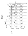
- One configuration using NMOS transistors involves an array in which each transistor is grounded at its source terminal 10 as shown in Figure 1 .
- PMOS transistors may be used, or a combination of both NMOS and PMOS.
- the transistors will typically be arranged in columns 11 and rows 12 as can be seen in Figure 1 .
- Transistors in the same row 12 will share a common gate connection 13, referred to herein as a word line.
- Transistors in the same column 11 will share a single output wire 14, referred to herein as a bit line.
- NMOS ROM Programming of the NMOS ROM shown in Figure 1 , is achieved by selectively connecting the bit lines 14 to the drain terminals 15 of the transistors in the array. A connection may be made by inserting a via 16 between a bit line and a drain. In an NMOS ROM, a via 16 programmes a "0" bit. Conversely, a non-connection 17 programmes a "1" bit.
- a ROM is read using the gate 18 and the drain 15 terminals of the transistors.
- all word lines 13 are grounded and the bit lines are pre-charged to V DD .
- the pre-charging circuitry is switched off and the appropriate word line 13 is activated, that is, a positive voltage V CC is applied to the word line. If there is a connection 16 between an activated transistor and a bit line, the voltage on the bit line will be pulled down to zero volts, and can be interpreted as a "0" in the data. If there is no connection 17 between an activated transistor and a bit line, the bit line will remain floating and will give a high voltage (a "1").
- the technique described above only allows for one bit of data to be stored per transistor. Since the density at which interconnects can be defined is much greater than the density at which transistors can be defined, it is desirable to create a ROM structure in which multiple bits may be stored per transistor. In such a structure, the bits may be encoded by means of multiple available configurations of interconnects to the transistor.
- One way of implementing the concept of storing multiple bits per transistor is to have multiple bit lines 24 for each column 21, as shown in Figure 2A .
- the number of bits that can be stored in each ROM cell is not proportional to the number of bit lines (X, Y, Z) per column. This is because connections to more than one bit line for a given transistor will short the different bit lines together and will not give a meaningful reading. This situation is shown as 22 in Figure 2A .
- the four states can be detected in a manner similar to that used for a standard single bit line ROM cell, as described above.
- the states can be decoded into a series of 2-bit words, as shown in the following truth table: Table 1 Configuration (see fig. 2 ) X Y Z Bit 1 Bit 2 25 1 1 1 0 0 26 0 1 1 0 1 27 1 0 1 1 0 28 1 1 0 1 1
- Table 1 is merely one example of one way in which the detected values may be decoded.
- a reading of "111" would mean that no connections were in place between the drain terminal of the transistor and the bit lines X, Y and Z.
- the state 111 would mean a word "00" had been encoded.
- a reading of "101” would mean that a via was in place between terminal Y and the drain terminal, and this would correspond to the word "10".
- US patents numbers US 6,355,550 and US 6,498,066 disclose ROMs using three bit lines per column.
- the ROMs are embedded in multi-layered integrated circuits.
- Figure 2B shows a representation of the possible connections in such prior art ROMs.
- "x" represents a position where a via may be placed in order to form a connection. Connections may be made at points 200, 201 or 202 between conductive pad 220 and bit lines 210, thus giving four possible states (200, 201, 202 or no connection).
- ROM cells such as those described above are typically fabricated using a series of masks and applying a series of patterned layers to a substrate. (See US 6,355,550 and US 6,498,066 .)
- bit lines are disconnected from V DD and instead bit line 1 is grounded and bit line 2 is left floating.
- V(bit line 1) 0
- V(bit line 2) V DD x C B2 /(C B2 + C C ), where C C is the capacitance between bit lines 1 and 2 through the dielectric substrate that separates them.
- C C is the capacitance between bit lines 1 and 2 through the dielectric substrate that separates them.
- this problem can be overcome by interleaving columns of bit cells and grounding bit lines associated with unused bit cells. For example, odd columns could be used for odd addresses and even columns for even addresses. In this way, at any given time the bit lines adjacent to a sensitive bit line will be grounded, and no coupling can occur.
- a further disadvantage that may be found with known multiple bit line ROMs is that several masks may need to be remade when a ROM is to be reprogrammed.
- a particular set of masks will be appropriate for a particular set of data to be programmed into a ROM, but when a different set of data need to be programmed several masks may need to be altered to produce different patterns on the substrate.
- a method for reading data stored in a multiple bit memory cell comprising a switch located within an array of switches arranged in columns and rows, each switch having a control node and first and second switched nodes between which the flow of current is dependent on the voltage applied to the control node, wherein each row has a word line connected to the control nodes of the switches of that row, each column comprises only one switch from each row, and each column has first, second and third bit lines connectable to one of the switched nodes of each switch of that column to define the stored data, the other of the switched nodes of each switch being connected to a reference voltage
- the method comprising: fixing the voltage of the second bit line of the switch and reading data from the first and third bit lines, and subsequently: fixing the voltage of the first bit line of the switch and reading data from the second and third bit lines.
- the steps of fixing the voltage of the first and second bit lines may comprise fixing the voltage of the respective line to the reference voltage. Alternatively, these steps may be replaced by steps of connecting the bit lines to a current sink.
- the second bit lines can suitably be positioned between the first and third bit lines such that they can provide shielding between the first and third bit lines.
- the steps of the first aspect of the present invention may constitute a single read operation.
- the switch is optionally a transistor.
- a multiple bit memory cell comprising a switch located within an array of switches arranged in columns and rows, each switch having a control node and first and second switched nodes between which the flow of current is dependent on the voltage applied to the control node, wherein each row has a word line connected to the control nodes of the switches of that row, each column comprises only one switch from each row, and each column has first, second and third bit lines connectable to one of the switched nodes of each switch of that column to define the stored data, the other of the switched nodes of each switch being connected to a reference voltage, the multiple bit memory cell being arranged to be read by fixing the voltage of the second bit line of the switch while reading data from the first and third bit lines, and subsequently fixing the voltage of the first bit line of the switch while reading data from the second and third bit lines.
- the second bit lines may be positioned between the first and third bit lines such that they can provide shielding between the first and third bit lines.
- the switch may be a transistor.
- the memory circuit may be a ROM circuit.
- Each cell may comprise a transistor that can be used for sensing the data content of the cell.
- the transistors are NMOS transistors.
- the transistors in each row have their gates connected to a word line of that row.
- the source of each transistor is connected to a reference voltage, conveniently ground.
- Each column includes a single transistor from each row.
- Each column has a number of bit lines, which can each independently be connected or not connected to the drain of each transistor in the column.
- the pattern of connections of the bit lines to the transistors defines the data stored in the ROM cell. As described above, to avoid shorts between the bit lines each transistor should be connected to no more than one of the bit lines.
- Figure 3 illustrates how charge sharing between adjacent bit lines can lead to false readings from ROMs.
- this problem is overcome in a multiple bit line ROM by treating separately the two encoded bits associated with each column, and reading each bit independently. By doing this, one of the three bit lines may be grounded while the other two remain active, and the coupling effect is thus reduced.
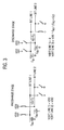
- Figure 4A shows the first stage of a method of reading data encoded in transistor 40 according to an embodiment of the invention.
- the middle bit line, Y is grounded while bit lines X and Z remain active. Coupling between bit lines X and Z is relatively unlikely because the capacitance between X and Z (which causes coupling problems) will always be much less than the capacitances between X and Y or between Z and Y (which reduce coupling effects).
- bit 2 may be accurately determined because the states resulting in bit 2 being high (or "1 "), i.e. states 001 and 100, are distinct from the states resulting in bit 2 being low (or "0"), i.e. states 101. As a result, bit 2 can be determined while bit line Y is grounded.
- bit line X reads zero in each state.
- the sensitive bit lines Y and Z are both high and therefore there will be no difficulty in establishing the values of these bit lines.
- coupling may occur between lines Y and Z it may not be possible to determine accurately whether the bit lines are high or low in states where one or more bit lines is low.
- bit 1 is high (00? and 0?0) can be distinguished from the states in which bit 1 is low (011).
- bit line Y will first be grounded while bit lines X and Z are read.
- the result will be state 101, as can be seen from Table 2. Referring to Table 2, state 101 may correspond to word 00 or to word 10 (the first and third states). Bit 2 must therefore be a 0.
- bit line X is grounded while lines Y and Z are read.
- the result should be state 001 (see Table 3); however, coupling may occur between lines Y and Z and bit line Z may lose some or all of its charge.
- bit line Z may be read as a 0 or a 1, and the result may therefore be 000.
- State 000 could also arise from encoding of word 11, as can be seen from Table 3.
- states 00? and 0?0 correspond to words 10 and 11 respectively, and bit 1 must therefore be a 1.
- the encoded word can be determined to be 10.
- bit line lay-out could be used in which the Y line does not provide physical shielding between X and Z.
- the truth table resulting from the Y line being grounded would be: Table 4 X Y Z Bit 1 Bit 2 1 0 1 0 0 0 0 0 ? 0 1 1 0 1 1 0 ? 0 0 1 1
- bit 2 is recoverable as it is from Table 2. Bit 2 will be a "0" only if X and Z are both "1". Bit 1 can then be recovered by grounding line X or line Z to produce the truth table of Table 3 or a corresponding table resulting from line Z being grounded.
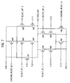
- the value "?” could denote a voltage between V CC and zero, i.e. a mid-rail voltage, because of a line losing part of its charge due to coupling.
- a mid-rail voltage When such a mid-rail voltage is applied to a logic gate, it could result in both NMOS and PMOS devices connected to the gate being turned on. This can cause a significant current drain, and is therefore undesirable.
- this situation can be avoided by careful design of the decoding logic, an example of which is shown in Figure 7 . In this arrangement, mid-rail voltage levels are avoided on one of the bit lines.
- transistor "ng1" will always be fully “off' and transistor “pg1” will always be fully “on”, and there will be no conduction from V DD to V SS .
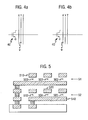
- Figures 5 and 6 show examples of three bit line ROMs.
- "x" represents a position where a via may be placed.
- connections may be made at positions 500, 501 or 502 between bit lines 510 and conductor 520, which might be a drain terminal of an NMOS transistor. Connections may also be made at positions 503, 504 or 505 between bit lines 530 and conductor 540.
- ROM of Figure 5 as in that of
- connections may be made at positions 600, 601 or 602 between bit lines 610 and conductor 620.
- only one mask layer 61 needs to be made to programme the ROM. This results in a substantial saving in the time and cost associated with programming ROMs.
- the exemplary NMOS ROM is shown in Figure 5 and has dimensions of 2.80 ⁇ m x 1.42 ⁇ m, giving an area of 3.976 ⁇ m 2 .
- Eight bits may be stored per cell (e.g. four 2-bit words), so that one bit requires approximately 0.5 ⁇ m 2 of the cell.
- the ROM will need to be at least (4x10 6 ) x 0.5 ⁇ m 2 , i.e. 2 mm 2 .
- the total area required to store 4Mbits of data, including core overhead, will be about 2.3 mm 2 .
- the exemplary ROM contains 0.18 ⁇ m NMOS transistors.
- transistors instead of transistors other forms of switch that permit current to flow from a first node (equivalent to the drain of the transistors described above) to a second node (equivalent to the source of the transistors described above) in dependence on the voltage applied to a control input (equivalent to the gate of the transistors described above) could be used.
- a control input equivalent to the gate of the transistors described above
Landscapes
- Engineering & Computer Science (AREA)
- Computer Hardware Design (AREA)
- Read Only Memory (AREA)
- Semiconductor Memories (AREA)
- For Increasing The Reliability Of Semiconductor Memories (AREA)
Claims (8)
- Procédé de lecture de données mémorisées dans une cellule mémoire à bits multiples, la cellule mémoire comprenant un commutateur (40) disposé dans un réseau de commutateurs agencé en colonnes et en rangées (11, 12), chaque commutateur comportant un noeud de commande (18) et des premier et deuxième noeuds commutés (10, 15) entre lesquels le courant dépend de la tension appliquée au noeud de commande, chaque rangée comportant une ligne de mots (13) connectée aux noeuds de commande des commutateurs de cette rangée, chaque colonne comprenant un seul commutateur pour chaque rangée, et chaque colonne comportant des première, deuxième et troisième lignes de bits (X, Y, Z) pouvant être connectées à l'un des noeuds commutés de chaque commutateur de cette colonne pour définir les données mémorisées, les autres noeuds commutés de chaque commutateur étant connectés à une tension de référence, le procédé comprenant les étapes suivantes :fixer la tension de la deuxième ligne de bits du commutateur tout en lisant des données dans les première et troisième lignes de bits ; et ensuitefixer la tension de la première ligne de bits du commutateur tout en lisant des données dans les deuxième et troisième lignes de bits.
- Procédé selon la revendication 1, dans lequel les étapes consistant à fixer la tension des première et deuxième lignes de bits incluent l'étape consistant à fixer la tension de la ligne respective à la tension de référence.
- Procédé selon la revendication 1 ou 2, dans lequel les deuxième lignes de bits sont disposées entre les première et troisième lignes de bits de sorte qu'elles peuvent assurer un écran entre les première et troisième lignes de bits.
- Procédé selon l'une quelconque des revendications précédentes, dans lequel les étapes décrites en revendication 1 constituent une seule opération de lecture.
- Procédé selon l'une quelconque des revendications précédentes, dans lequel le commutateur est un transistor.
- Cellule mémoire à bits multiples comprenant un commutateur (40) disposé dans un réseau de commutateurs agencé en colonnes et rangées (11, 12), chaque commutateur comportant un noeud de commande (18) et des premier et deuxième noeuds commutés (10, 15) entre lesquels le courant dépend de la tension appliquée au noeud de commande, chaque rangée comportant une ligne de mots (13) connectée aux noeuds de commande des commutateurs de cette rangée, chaque colonne comprenant au moins un commutateur à partir de chaque rangée, et chaque colonne comportant des première, deuxième et troisième lignes de bits (X, Y, Z) pouvant être connectées à l'un des noeuds commutés de chaque commutateur de cette colonne pour définir les données mémorisées, les autres noeuds commutés de chaque commutateur étant connectés à une tension de référence,
caractérisée en ce que la cellule mémoire à bits multiples est agencée pour être lue par les étapes suivantes :fixer la tension de la deuxième ligne de bits du commutateur tout en lisant des données des première et troisième lignes de bits ; et ensuitefixer la tension de la première ligne de bits du commutateur tout en lisant des données des deuxième et troisième lignes de bits. - Cellule mémoire à bits multiples selon la revendication 6, dans laquelle les deuxièmes lignes de bits sont disposées entre les première et troisième lignes de bits de sorte qu'elles peuvent assurer un écran entre les première et troisième lignes de bits.
- Cellule mémoire à bits multiples selon la revendication 6 ou 7, dans laquelle le commutateur est un transistor.
Applications Claiming Priority (2)
| Application Number | Priority Date | Filing Date | Title |
|---|---|---|---|
| GBGB0406038.0A GB0406038D0 (en) | 2004-03-17 | 2004-03-17 | Method for reading rom cell |
| GB0406038 | 2004-03-17 |
Publications (3)
| Publication Number | Publication Date |
|---|---|
| EP1577898A2 EP1577898A2 (fr) | 2005-09-21 |
| EP1577898A3 EP1577898A3 (fr) | 2006-08-30 |
| EP1577898B1 true EP1577898B1 (fr) | 2008-08-13 |
Family
ID=32117901
Family Applications (1)
| Application Number | Title | Priority Date | Filing Date |
|---|---|---|---|
| EP05251525A Expired - Lifetime EP1577898B1 (fr) | 2004-03-17 | 2005-03-14 | Procédé de lecture des cellules ROM multibits |
Country Status (5)
| Country | Link |
|---|---|
| US (1) | US7411808B2 (fr) |
| EP (1) | EP1577898B1 (fr) |
| AT (1) | ATE404975T1 (fr) |
| DE (1) | DE602005008788D1 (fr) |
| GB (1) | GB0406038D0 (fr) |
Families Citing this family (8)
| Publication number | Priority date | Publication date | Assignee | Title |
|---|---|---|---|---|
| US7324364B2 (en) | 2006-02-27 | 2008-01-29 | Agere Systems Inc. | Layout techniques for memory circuitry |
| US7301828B2 (en) * | 2006-02-27 | 2007-11-27 | Agere Systems Inc. | Decoding techniques for read-only memory |
| FR2915019B1 (fr) * | 2007-04-13 | 2009-07-17 | Dolphin Integration Sa | Memoire rom multibit |
| US7816875B2 (en) * | 2008-01-24 | 2010-10-19 | Viking Access Systems, Llc | High torque gearless actuation at low speeds for swing gate, roll-up gate, slide gate, and vehicular barrier operators |
| JP2010010369A (ja) * | 2008-06-26 | 2010-01-14 | Panasonic Corp | 混載メモリ装置及び半導体装置 |
| JP6122801B2 (ja) * | 2014-03-13 | 2017-04-26 | 株式会社東芝 | 半導体記憶装置 |
| US11152060B2 (en) * | 2019-06-21 | 2021-10-19 | Intel Corporation | Multi-bit read-only memory device |
| CN114300028B (zh) * | 2021-12-14 | 2023-06-16 | 成都海光微电子技术有限公司 | Rom存储单元及rom存储单元存储信息的读取方法 |
Family Cites Families (6)
| Publication number | Priority date | Publication date | Assignee | Title |
|---|---|---|---|---|
| US5870326A (en) * | 1997-08-12 | 1999-02-09 | Intel Corporation | Information encoding by multiple line selection |
| US6002607A (en) * | 1998-02-24 | 1999-12-14 | National Semiconductor Corporation | Read-only-memory (ROM) having a memory cell that stores a plurality of bits of information |
| FR2794895B1 (fr) * | 1999-06-11 | 2001-09-14 | St Microelectronics Sa | Dispositif semiconducteur integre de memoire morte |
| US6355550B1 (en) * | 2000-05-19 | 2002-03-12 | Motorola, Inc. | Ultra-late programming ROM and method of manufacture |
| FR2826170B1 (fr) * | 2001-06-15 | 2003-12-12 | Dolphin Integration Sa | Memoire rom a points memoire multibit |
| US6590797B1 (en) * | 2002-01-09 | 2003-07-08 | Tower Semiconductor Ltd. | Multi-bit programmable memory cell having multiple anti-fuse elements |
-
2004
- 2004-03-17 GB GBGB0406038.0A patent/GB0406038D0/en not_active Ceased
-
2005
- 2005-03-14 DE DE602005008788T patent/DE602005008788D1/de not_active Expired - Lifetime
- 2005-03-14 AT AT05251525T patent/ATE404975T1/de not_active IP Right Cessation
- 2005-03-14 EP EP05251525A patent/EP1577898B1/fr not_active Expired - Lifetime
- 2005-03-16 US US11/080,493 patent/US7411808B2/en not_active Expired - Fee Related
Also Published As
| Publication number | Publication date |
|---|---|
| EP1577898A2 (fr) | 2005-09-21 |
| US7411808B2 (en) | 2008-08-12 |
| US20050213362A1 (en) | 2005-09-29 |
| DE602005008788D1 (de) | 2008-09-25 |
| GB0406038D0 (en) | 2004-04-21 |
| EP1577898A3 (fr) | 2006-08-30 |
| ATE404975T1 (de) | 2008-08-15 |
Similar Documents
| Publication | Publication Date | Title |
|---|---|---|
| US7177227B2 (en) | Transistor layout configuration for tight-pitched memory array lines | |
| KR101204021B1 (ko) | 메모리 라인 구동기의 비-이진 그룹에 대한 디코딩 회로 | |
| EP0939444B1 (fr) | Structure d'accès pour mémoire morte à haute densité | |
| EP1864291B1 (fr) | Procede et appareil pour incorporer une redondance de blocs dans une matrice memoire | |
| CN100511474C (zh) | 开放式位线dram结构的噪声抑制 | |
| KR100304750B1 (ko) | 반도체기억장치 | |
| EP1938331B1 (fr) | Configuration de matrice memoire de circuit integre comportant une compatibilite de decodage avec mise en oeuvre partielle de couches memoires multiples | |
| US5625586A (en) | Semiconductor memory having a plurality of memory banks and sub-bit lines which are connected to a main bit line via MOS transistors whose gates are commonly connected to a selection line | |
| KR0179361B1 (ko) | 비휘발성 메모리 어레이 | |
| EP0225499B1 (fr) | Méthode à graine et maille pour réseaux intégrés | |
| KR20030059120A (ko) | Mtj mram 병렬-병렬 아키텍쳐 | |
| EP1435098B1 (fr) | Architecture de ligne mot et de ligne bit dans une memoire vive magnetique | |
| EP1577898B1 (fr) | Procédé de lecture des cellules ROM multibits | |
| KR100379289B1 (ko) | 낮은 임계 전압치와 개선된 패턴 형상을 가진트랜지스터를 구비한 논리회로를 가진 반도체 집적회로 | |
| US5870326A (en) | Information encoding by multiple line selection | |
| JPS63160358A (ja) | Cmosゲートアレイ内の高密度rom | |
| US6556468B2 (en) | High bit density, high speed, via and metal programmable read only memory core cell architecture | |
| JP2005513691A6 (ja) | 半記憶密度rom内蔵dram | |
| JP2005513691A (ja) | 半記憶密度rom内蔵dram | |
| USRE33280E (en) | Semiconductor memory device | |
| US7161824B2 (en) | Method for programming a memory arrangement and programmed memory arrangement | |
| EP0886279B1 (fr) | Décodeur d'adresse, mémoire à semiconducteurs et dispositif à semiconducteurs | |
| US10236071B1 (en) | Dual-bit ROM cell with virtual ground line and programmable metal track | |
| US20120327698A1 (en) | Interconnection architecture for memory structures | |
| KR100868035B1 (ko) | 메모리 회로, 메모리 회로를 동작시키는 방법, 메모리디바이스 및 메모리 디바이스를 생성하는 방법 |
Legal Events
| Date | Code | Title | Description |
|---|---|---|---|
| PUAI | Public reference made under article 153(3) epc to a published international application that has entered the european phase |
Free format text: ORIGINAL CODE: 0009012 |
|
| AK | Designated contracting states |
Kind code of ref document: A2 Designated state(s): AT BE BG CH CY CZ DE DK EE ES FI FR GB GR HU IE IS IT LI LT LU MC NL PL PT RO SE SI SK TR |
|
| AX | Request for extension of the european patent |
Extension state: AL BA HR LV MK YU |
|
| PUAL | Search report despatched |
Free format text: ORIGINAL CODE: 0009013 |
|
| AK | Designated contracting states |
Kind code of ref document: A3 Designated state(s): AT BE BG CH CY CZ DE DK EE ES FI FR GB GR HU IE IS IT LI LT LU MC NL PL PT RO SE SI SK TR |
|
| AX | Request for extension of the european patent |
Extension state: AL BA HR LV MK YU |
|
| 17P | Request for examination filed |
Effective date: 20070219 |
|
| 17Q | First examination report despatched |
Effective date: 20070319 |
|
| AKX | Designation fees paid |
Designated state(s): AT BE BG CH CY CZ DE DK EE ES FI FR GB GR HU IE IS IT LI LT LU MC NL PL PT RO SE SI SK TR |
|
| GRAP | Despatch of communication of intention to grant a patent |
Free format text: ORIGINAL CODE: EPIDOSNIGR1 |
|
| GRAS | Grant fee paid |
Free format text: ORIGINAL CODE: EPIDOSNIGR3 |
|
| GRAA | (expected) grant |
Free format text: ORIGINAL CODE: 0009210 |
|
| AK | Designated contracting states |
Kind code of ref document: B1 Designated state(s): AT BE BG CH CY CZ DE DK EE ES FI FR GB GR HU IE IS IT LI LT LU MC NL PL PT RO SE SI SK TR |
|
| REG | Reference to a national code |
Ref country code: GB Ref legal event code: FG4D |
|
| REG | Reference to a national code |
Ref country code: CH Ref legal event code: EP |
|
| REG | Reference to a national code |
Ref country code: IE Ref legal event code: FG4D |
|
| REF | Corresponds to: |
Ref document number: 602005008788 Country of ref document: DE Date of ref document: 20080925 Kind code of ref document: P |
|
| REG | Reference to a national code |
Ref country code: SE Ref legal event code: TRGR |
|
| PG25 | Lapsed in a contracting state [announced via postgrant information from national office to epo] |
Ref country code: LT Free format text: LAPSE BECAUSE OF FAILURE TO SUBMIT A TRANSLATION OF THE DESCRIPTION OR TO PAY THE FEE WITHIN THE PRESCRIBED TIME-LIMIT Effective date: 20080813 Ref country code: IS Free format text: LAPSE BECAUSE OF FAILURE TO SUBMIT A TRANSLATION OF THE DESCRIPTION OR TO PAY THE FEE WITHIN THE PRESCRIBED TIME-LIMIT Effective date: 20081213 |
|
| PG25 | Lapsed in a contracting state [announced via postgrant information from national office to epo] |
Ref country code: ES Free format text: LAPSE BECAUSE OF FAILURE TO SUBMIT A TRANSLATION OF THE DESCRIPTION OR TO PAY THE FEE WITHIN THE PRESCRIBED TIME-LIMIT Effective date: 20081124 Ref country code: AT Free format text: LAPSE BECAUSE OF FAILURE TO SUBMIT A TRANSLATION OF THE DESCRIPTION OR TO PAY THE FEE WITHIN THE PRESCRIBED TIME-LIMIT Effective date: 20080813 Ref country code: SI Free format text: LAPSE BECAUSE OF FAILURE TO SUBMIT A TRANSLATION OF THE DESCRIPTION OR TO PAY THE FEE WITHIN THE PRESCRIBED TIME-LIMIT Effective date: 20080813 |
|
| PG25 | Lapsed in a contracting state [announced via postgrant information from national office to epo] |
Ref country code: BE Free format text: LAPSE BECAUSE OF FAILURE TO SUBMIT A TRANSLATION OF THE DESCRIPTION OR TO PAY THE FEE WITHIN THE PRESCRIBED TIME-LIMIT Effective date: 20080813 |
|
| PG25 | Lapsed in a contracting state [announced via postgrant information from national office to epo] |
Ref country code: BG Free format text: LAPSE BECAUSE OF FAILURE TO SUBMIT A TRANSLATION OF THE DESCRIPTION OR TO PAY THE FEE WITHIN THE PRESCRIBED TIME-LIMIT Effective date: 20081113 Ref country code: DK Free format text: LAPSE BECAUSE OF FAILURE TO SUBMIT A TRANSLATION OF THE DESCRIPTION OR TO PAY THE FEE WITHIN THE PRESCRIBED TIME-LIMIT Effective date: 20080813 |
|
| PG25 | Lapsed in a contracting state [announced via postgrant information from national office to epo] |
Ref country code: SK Free format text: LAPSE BECAUSE OF FAILURE TO SUBMIT A TRANSLATION OF THE DESCRIPTION OR TO PAY THE FEE WITHIN THE PRESCRIBED TIME-LIMIT Effective date: 20080813 Ref country code: PT Free format text: LAPSE BECAUSE OF FAILURE TO SUBMIT A TRANSLATION OF THE DESCRIPTION OR TO PAY THE FEE WITHIN THE PRESCRIBED TIME-LIMIT Effective date: 20090113 Ref country code: CZ Free format text: LAPSE BECAUSE OF FAILURE TO SUBMIT A TRANSLATION OF THE DESCRIPTION OR TO PAY THE FEE WITHIN THE PRESCRIBED TIME-LIMIT Effective date: 20080813 Ref country code: RO Free format text: LAPSE BECAUSE OF FAILURE TO SUBMIT A TRANSLATION OF THE DESCRIPTION OR TO PAY THE FEE WITHIN THE PRESCRIBED TIME-LIMIT Effective date: 20080813 |
|
| PLBE | No opposition filed within time limit |
Free format text: ORIGINAL CODE: 0009261 |
|
| STAA | Information on the status of an ep patent application or granted ep patent |
Free format text: STATUS: NO OPPOSITION FILED WITHIN TIME LIMIT |
|
| 26N | No opposition filed |
Effective date: 20090514 |
|
| PG25 | Lapsed in a contracting state [announced via postgrant information from national office to epo] |
Ref country code: EE Free format text: LAPSE BECAUSE OF FAILURE TO SUBMIT A TRANSLATION OF THE DESCRIPTION OR TO PAY THE FEE WITHIN THE PRESCRIBED TIME-LIMIT Effective date: 20080813 |
|
| PG25 | Lapsed in a contracting state [announced via postgrant information from national office to epo] |
Ref country code: IT Free format text: LAPSE BECAUSE OF FAILURE TO SUBMIT A TRANSLATION OF THE DESCRIPTION OR TO PAY THE FEE WITHIN THE PRESCRIBED TIME-LIMIT Effective date: 20080813 |
|
| PG25 | Lapsed in a contracting state [announced via postgrant information from national office to epo] |
Ref country code: MC Free format text: LAPSE BECAUSE OF NON-PAYMENT OF DUE FEES Effective date: 20090331 |
|
| REG | Reference to a national code |
Ref country code: CH Ref legal event code: PL |
|
| REG | Reference to a national code |
Ref country code: IE Ref legal event code: MM4A |
|
| PG25 | Lapsed in a contracting state [announced via postgrant information from national office to epo] |
Ref country code: CH Free format text: LAPSE BECAUSE OF NON-PAYMENT OF DUE FEES Effective date: 20090331 Ref country code: IE Free format text: LAPSE BECAUSE OF NON-PAYMENT OF DUE FEES Effective date: 20090314 Ref country code: LI Free format text: LAPSE BECAUSE OF NON-PAYMENT OF DUE FEES Effective date: 20090331 |
|
| PG25 | Lapsed in a contracting state [announced via postgrant information from national office to epo] |
Ref country code: PL Free format text: LAPSE BECAUSE OF FAILURE TO SUBMIT A TRANSLATION OF THE DESCRIPTION OR TO PAY THE FEE WITHIN THE PRESCRIBED TIME-LIMIT Effective date: 20080813 |
|
| PG25 | Lapsed in a contracting state [announced via postgrant information from national office to epo] |
Ref country code: GR Free format text: LAPSE BECAUSE OF FAILURE TO SUBMIT A TRANSLATION OF THE DESCRIPTION OR TO PAY THE FEE WITHIN THE PRESCRIBED TIME-LIMIT Effective date: 20081114 |
|
| PG25 | Lapsed in a contracting state [announced via postgrant information from national office to epo] |
Ref country code: LU Free format text: LAPSE BECAUSE OF NON-PAYMENT OF DUE FEES Effective date: 20090314 |
|
| PG25 | Lapsed in a contracting state [announced via postgrant information from national office to epo] |
Ref country code: HU Free format text: LAPSE BECAUSE OF FAILURE TO SUBMIT A TRANSLATION OF THE DESCRIPTION OR TO PAY THE FEE WITHIN THE PRESCRIBED TIME-LIMIT Effective date: 20090214 |
|
| PG25 | Lapsed in a contracting state [announced via postgrant information from national office to epo] |
Ref country code: TR Free format text: LAPSE BECAUSE OF FAILURE TO SUBMIT A TRANSLATION OF THE DESCRIPTION OR TO PAY THE FEE WITHIN THE PRESCRIBED TIME-LIMIT Effective date: 20080813 |
|
| PG25 | Lapsed in a contracting state [announced via postgrant information from national office to epo] |
Ref country code: CY Free format text: LAPSE BECAUSE OF FAILURE TO SUBMIT A TRANSLATION OF THE DESCRIPTION OR TO PAY THE FEE WITHIN THE PRESCRIBED TIME-LIMIT Effective date: 20080813 |
|
| REG | Reference to a national code |
Ref country code: DE Ref legal event code: R082 Ref document number: 602005008788 Country of ref document: DE Representative=s name: OLSWANG GERMANY LLP, DE Ref country code: DE Ref legal event code: R082 Ref document number: 602005008788 Country of ref document: DE Representative=s name: MAUCHER JENKINS, DE |
|
| PGFP | Annual fee paid to national office [announced via postgrant information from national office to epo] |
Ref country code: FI Payment date: 20130327 Year of fee payment: 9 Ref country code: SE Payment date: 20130327 Year of fee payment: 9 |
|
| PGFP | Annual fee paid to national office [announced via postgrant information from national office to epo] |
Ref country code: NL Payment date: 20130326 Year of fee payment: 9 |
|
| REG | Reference to a national code |
Ref country code: NL Ref legal event code: V1 Effective date: 20141001 |
|
| PG25 | Lapsed in a contracting state [announced via postgrant information from national office to epo] |
Ref country code: FI Free format text: LAPSE BECAUSE OF NON-PAYMENT OF DUE FEES Effective date: 20140314 |
|
| REG | Reference to a national code |
Ref country code: SE Ref legal event code: EUG |
|
| PG25 | Lapsed in a contracting state [announced via postgrant information from national office to epo] |
Ref country code: SE Free format text: LAPSE BECAUSE OF NON-PAYMENT OF DUE FEES Effective date: 20140315 |
|
| PG25 | Lapsed in a contracting state [announced via postgrant information from national office to epo] |
Ref country code: NL Free format text: LAPSE BECAUSE OF NON-PAYMENT OF DUE FEES Effective date: 20141001 |
|
| REG | Reference to a national code |
Ref country code: FR Ref legal event code: PLFP Year of fee payment: 11 |
|
| REG | Reference to a national code |
Ref country code: DE Ref legal event code: R082 Ref document number: 602005008788 Country of ref document: DE Representative=s name: MAUCHER JENKINS PATENTANWAELTE & RECHTSANWAELT, DE Ref country code: DE Ref legal event code: R082 Ref document number: 602005008788 Country of ref document: DE Representative=s name: MAUCHER JENKINS, DE Ref country code: DE Ref legal event code: R082 Ref document number: 602005008788 Country of ref document: DE Representative=s name: OLSWANG GERMANY LLP, DE Ref country code: DE Ref legal event code: R081 Ref document number: 602005008788 Country of ref document: DE Owner name: QUALCOMM TECHNOLOGIES INTERNATIONAL, LTD., GB Free format text: FORMER OWNER: CAMBRIDGE SILICON RADIO LTD., CAMBRIDGE, CAMBRIDGESHIRE, GB |
|
| REG | Reference to a national code |
Ref country code: FR Ref legal event code: PLFP Year of fee payment: 12 |
|
| REG | Reference to a national code |
Ref country code: FR Ref legal event code: CD Owner name: QUALCOMM TECHNOLOGIES INTERNATIONAL, LTD., GB Effective date: 20160201 |
|
| REG | Reference to a national code |
Ref country code: FR Ref legal event code: PLFP Year of fee payment: 13 |
|
| REG | Reference to a national code |
Ref country code: DE Ref legal event code: R082 Ref document number: 602005008788 Country of ref document: DE Representative=s name: MAUCHER JENKINS PATENTANWAELTE & RECHTSANWAELT, DE Ref country code: DE Ref legal event code: R082 Ref document number: 602005008788 Country of ref document: DE Representative=s name: MAUCHER JENKINS, DE |
|
| REG | Reference to a national code |
Ref country code: FR Ref legal event code: PLFP Year of fee payment: 14 |
|
| PGFP | Annual fee paid to national office [announced via postgrant information from national office to epo] |
Ref country code: GB Payment date: 20180223 Year of fee payment: 14 Ref country code: DE Payment date: 20180308 Year of fee payment: 14 |
|
| PGFP | Annual fee paid to national office [announced via postgrant information from national office to epo] |
Ref country code: FR Payment date: 20180223 Year of fee payment: 14 |
|
| REG | Reference to a national code |
Ref country code: DE Ref legal event code: R119 Ref document number: 602005008788 Country of ref document: DE |
|
| GBPC | Gb: european patent ceased through non-payment of renewal fee |
Effective date: 20190314 |
|
| PG25 | Lapsed in a contracting state [announced via postgrant information from national office to epo] |
Ref country code: DE Free format text: LAPSE BECAUSE OF NON-PAYMENT OF DUE FEES Effective date: 20191001 Ref country code: GB Free format text: LAPSE BECAUSE OF NON-PAYMENT OF DUE FEES Effective date: 20190314 |
|
| PG25 | Lapsed in a contracting state [announced via postgrant information from national office to epo] |
Ref country code: FR Free format text: LAPSE BECAUSE OF NON-PAYMENT OF DUE FEES Effective date: 20190331 |