EP1576348B1 - (high) pressure sensor featuring pressure loading of the fastening element - Google Patents
(high) pressure sensor featuring pressure loading of the fastening element Download PDFInfo
- Publication number
- EP1576348B1 EP1576348B1 EP03813524A EP03813524A EP1576348B1 EP 1576348 B1 EP1576348 B1 EP 1576348B1 EP 03813524 A EP03813524 A EP 03813524A EP 03813524 A EP03813524 A EP 03813524A EP 1576348 B1 EP1576348 B1 EP 1576348B1
- Authority
- EP
- European Patent Office
- Prior art keywords
- pressure sensor
- pressure
- fastening
- sensor element
- sensor according
- Prior art date
- Legal status (The legal status is an assumption and is not a legal conclusion. Google has not performed a legal analysis and makes no representation as to the accuracy of the status listed.)
- Expired - Lifetime
Links
- 239000012528 membrane Substances 0.000 claims description 23
- 239000000463 material Substances 0.000 claims description 15
- 239000004065 semiconductor Substances 0.000 claims description 4
- 230000001154 acute effect Effects 0.000 claims description 3
- XUIMIQQOPSSXEZ-UHFFFAOYSA-N Silicon Chemical compound [Si] XUIMIQQOPSSXEZ-UHFFFAOYSA-N 0.000 description 15
- 229910052710 silicon Inorganic materials 0.000 description 15
- 239000010703 silicon Substances 0.000 description 15
- 239000000758 substrate Substances 0.000 description 9
- 238000005530 etching Methods 0.000 description 6
- 239000011521 glass Substances 0.000 description 6
- 238000004519 manufacturing process Methods 0.000 description 6
- 238000010276 construction Methods 0.000 description 4
- 239000002184 metal Substances 0.000 description 4
- 238000000034 method Methods 0.000 description 4
- 229910000679 solder Inorganic materials 0.000 description 4
- 238000011156 evaluation Methods 0.000 description 3
- 230000000694 effects Effects 0.000 description 2
- 238000007373 indentation Methods 0.000 description 2
- 229910000833 kovar Inorganic materials 0.000 description 2
- 230000009172 bursting Effects 0.000 description 1
- 239000013078 crystal Substances 0.000 description 1
- 230000001419 dependent effect Effects 0.000 description 1
- 239000003292 glue Substances 0.000 description 1
- 238000001746 injection moulding Methods 0.000 description 1
- 239000003921 oil Substances 0.000 description 1
- 238000000926 separation method Methods 0.000 description 1
- 239000007921 spray Substances 0.000 description 1
- 239000010409 thin film Substances 0.000 description 1
Images

Classifications
-
- G—PHYSICS
- G01—MEASURING; TESTING
- G01L—MEASURING FORCE, STRESS, TORQUE, WORK, MECHANICAL POWER, MECHANICAL EFFICIENCY, OR FLUID PRESSURE
- G01L19/00—Details of, or accessories for, apparatus for measuring steady or quasi-steady pressure of a fluent medium insofar as such details or accessories are not special to particular types of pressure gauges
- G01L19/14—Housings
- G01L19/148—Details about the circuit board integration, e.g. integrated with the diaphragm surface or encapsulation
-
- G—PHYSICS
- G01—MEASURING; TESTING
- G01L—MEASURING FORCE, STRESS, TORQUE, WORK, MECHANICAL POWER, MECHANICAL EFFICIENCY, OR FLUID PRESSURE
- G01L19/00—Details of, or accessories for, apparatus for measuring steady or quasi-steady pressure of a fluent medium insofar as such details or accessories are not special to particular types of pressure gauges
- G01L19/14—Housings
- G01L19/147—Details about the mounting of the sensor to support or covering means
-
- H—ELECTRICITY
- H01—ELECTRIC ELEMENTS
- H01L—SEMICONDUCTOR DEVICES NOT COVERED BY CLASS H10
- H01L2224/00—Indexing scheme for arrangements for connecting or disconnecting semiconductor or solid-state bodies and methods related thereto as covered by H01L24/00
- H01L2224/01—Means for bonding being attached to, or being formed on, the surface to be connected, e.g. chip-to-package, die-attach, "first-level" interconnects; Manufacturing methods related thereto
- H01L2224/42—Wire connectors; Manufacturing methods related thereto
- H01L2224/47—Structure, shape, material or disposition of the wire connectors after the connecting process
- H01L2224/48—Structure, shape, material or disposition of the wire connectors after the connecting process of an individual wire connector
- H01L2224/4805—Shape
- H01L2224/4809—Loop shape
- H01L2224/48091—Arched
-
- H—ELECTRICITY
- H01—ELECTRIC ELEMENTS
- H01L—SEMICONDUCTOR DEVICES NOT COVERED BY CLASS H10
- H01L2924/00—Indexing scheme for arrangements or methods for connecting or disconnecting semiconductor or solid-state bodies as covered by H01L24/00
- H01L2924/10—Details of semiconductor or other solid state devices to be connected
- H01L2924/102—Material of the semiconductor or solid state bodies
- H01L2924/1025—Semiconducting materials
- H01L2924/10251—Elemental semiconductors, i.e. Group IV
- H01L2924/10253—Silicon [Si]
Definitions
- the invention is based on a pressure sensor according to the preamble of the main claim.
- Micromechanical silicon pressure sensors are already known, a membrane being produced by the introduction of a cavern in a silicon chip.
- a silicon sensor is disclosed, for example, in German Offenlegungsschrift DE 199 57 556 disclosed.
- the cavern is generated for example by anisotropic KOH etching.
- the font DE 199 29 026 A1 shows a method for producing a pressure sensor, in which a stamp is placed on the membrane to protect the membrane of a pressure sensor element before the pressure sensor element is surrounded with a spray mass.
- the pressure sensor according to the invention with the features of the main claim has the advantage that a simple and inexpensive construction for the production of a pressure sensor is proposed.
- the pressure sensor according to the invention is used to measure high pressures, wherein the pressure sensor according to the invention nevertheless has a high overload safety.
- the pressure sensor according to the invention has the advantage that a cost-effective production of a micromechanical sensor for low to high pressures (up to or over 1000 bar) is possible. This makes it possible to inexpensively provide a pressure sensor that can be used for a wide range of different pressures. As a result, the numbers can be increased and the costs can be further reduced.
- the inventive arrangement it is also possible to effect a separation of pressure medium and evaluation circuit.
- the pressure sensor element is made of semiconductor material and / or produced in bulk micromechanics. This makes it possible to produce the pressure sensor element and thus the pressure sensor particularly cost-effective and reliable. Furthermore, it is advantageous that the pressure sensor is provided for high pressures up to about 1000 bar or for high pressures above 1000 bar. As a result, the pressure sensor is particularly cost-effective and can be produced in large quantities because of its usability in a large pressure range. Furthermore, it is advantageous that the fastening element is provided with respect to its temperature coefficient of expansion to the sensor element adapted. As a result, it is possible that due to temperature fluctuations only small voltages are introduced into the sensor element or that the pressure sensor can be used not only in a large pressure range but also in a wide temperature range.
- a connecting material is provided between the first fastening region and the second fastening region, wherein the connecting material is provided in particular comparatively soft.
- the connecting material is provided in particular comparatively soft.
- resistance elements are provided in the membrane region. This makes it possible with simple means and thus cost-effective to measure pressures in large pressure ranges.
- the connection surface between the first attachment region and the second attachment region is provided parallel or obliquely or at an acute angle to the membrane plane. This results in many possible variations of the pressure sensor according to the invention.
- the cross section of the fastening element tapers towards the second fastening region. This makes it possible to mount the sensor chip centered in a simple manner.
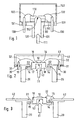
- FIG. 1 a known micromechanical silicon pressure sensor according to the prior art
- FIG. 2 a pressure sensor according to the invention as absolute pressure sensor
- FIG. 3 a pressure sensor according to the invention as a relative pressure sensor
- FIG. 4 various intermediate steps for the production of the sensor element
- FIG. 5 a first construction variant of the sensor according to the invention
- FIG. 6 a second construction variant of the sensor according to the invention.
- FIG. 1 the general construction of micromechanical silicon pressure sensors is shown.
- a silicon substrate 110 is provided with a cavern 152, which leaves a membrane not provided with a reference numeral.
- the silicon substrate 110 is connected to a bored glass 150, which is soldered to a base 120 with a solder 160.
- the base 120 is integrally connected to a pressure connection pipe 120.
- measuring resistors not provided with a reference mark and located on the upper side of the silicon substrate 110 are connected via one or more bonding wires 132 to a connection pin 130, which are electrically separated from the base 120 by means of an indentation 131.
- the cavity 152 of the silicon substrate 110 has a typical etched slope that is approximately truncated pyramid-shaped. This results in a trapezoidal cross-section.
- This truncated pyramidal recess below the sensor membrane results from the use of a silicon substrate which has a (100) orientation because a KOH etch has different etch rates in different crystal directions. It proves to be disadvantageous in the known pressure sensor that the truncated pyramidal recess at its largest cross-section, ie at the rear side of the silicon substrate, is decisive as the pressure-engaging surface. As a result, large tensile forces act on the glass 150 and the solder 160. As a result, the silicon sensor in the prior art has only a comparatively low bursting pressure. Pressure sensors are often manufactured in bulk micromechanics and anodically bonded to glass. For back pressure, the sensor is soldered to a perforated socket.
- FIG. 2 a pressure sensor is shown.
- a pressure sensor element 10 which is provided in particular of a semiconductor material and in particular of silicon, has a membrane region 12 on a front side.
- an etched cavern 52 is formed in the pressure sensor element 10, which in particular by means of a Trenchiserbacters from the back into the pressure sensor element 10th was introduced.
- FIG. 2 are indicated by the reference numeral 16 measuring resistors on the diaphragm portion 12 of the pressure sensor element 10, which are not shown in the other figures for the sake of simplicity, however, to be included.
- the pressure sensor element 10 has in FIG. 2 in the region of its rear side, a fastening region 14, which is referred to below as the first fastening region 14.
- the pressure sensor chip 10, ie the pressure sensor element 10, is in the in FIG. 2 illustrated embodiment, in particular made so that it has lateral projections 17, by means of which it can be fixed in or on a base 20. With this type of fastening, only compressive stresses occur when pressurized.
- the force exerted by the pressurization on the pressure sensor element 10 is in FIG. 2 shown with an arrow and the reference numeral 11.
- the pressure sensor element 10 is connected to the base 20, wherein the base 20 is also referred to below as a fastening element 20.
- the fastening element 20 likewise has a fastening region 22, in particular in the region of the aforementioned projection 17, which is referred to below as the second fastening region 22.
- a connection material 15 is provided between the first attachment portion 14 and the second attachment portion 22.
- connecting material 15 e.g. Solder (metal, glass) or glue can be used.
- the base 20 is made of the material Kovar and is thus in terms of its thermal expansion coefficient of the thermal expansion coefficient of the material of the pressure sensor element 10, i. in particular to silicon. Since the preferred base material Kovar is poorly workable, the base 20 is preferably manufactured by the technique of "metal injection molding".
- the connecting material 15 is preferably relatively soft to absorb mechanical stresses during temperature changes.
- FIG. 2 an embodiment of the pressure sensor is shown as an absolute pressure sensor.
- a vacuum-tight cap 40 is provided around the front of the pressure sensor element 10.
- the base 20 in turn comprises in its lower part and not shown in detail by a reference numeral a pressure connection pipe.
- the measuring resistors 12 located on the upper side of the pressure sensor element 10 are connected via one or more bonding wires 32 to one or more connecting pins 30, which are electrically separated from the base 20 by means of an indentation 31.
- the cap 40 encloses a reference volume 41, which is provided for example evacuated.
- FIG. 3 a pressure sensor is shown as a relative pressure sensor.
- the pressure sensor element 10 is shown with its first attachment region 14 and its membrane region 12.
- the base 20 is shown with its second mounting portion 22.
- the connecting material 15 between the first and the second attachment region 14, 22 and the pressure force 11 or force 11 exerted on the pressure sensor element 10 are again shown.
- the reference numeral 42 a circuit board.
- the electrical feeds between the printed circuit board 42 and the pressure sensor element 10 are in turn realized via bonding wires 32.
- the circuit board 42 may be provided according to the invention as a hybrid 42.
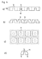
- FIG. 4 various intermediate steps for the production of the sensor element 10 are shown.
- a substrate 50 in particular a semiconductor substrate 50 as a preferred material for the sensor element 10 is processed in accordance with known methods.
- a cavern 52 is etched into the rear side of the future pressure sensor element 10, cf.
- FIG. 4a In this case, according to the invention, in particular, a trench etching method or a - as in connection with FIG. 1 explained - KOH etching application.
- a trench etching method or a - as in connection with FIG. 1 explained - KOH etching application.
- prior to the etching of the cavern 52 on the front side of the future pressure sensor element 10 piezoresistive resistances on the membrane and possibly additionally an integrated Evaluation circuit generated in the substrate 50 adjacent to the membrane.
- FIG. 4b a further step for manufacturing the pressure sensor elements 10 is shown: notches 54 are realized from the front side.
- Figure 4a and Figure 4b each represent side views of the pressure sensor element 10 according to the invention along a section through the membrane region 12.
- the notches 54 are produced in particular by etching techniques such as high-rate etching or sawing with a wide saw blade.
- the shape of the notches, such as square, round, etc., is freely selectable.
- FIG. 2 illustrates a top view of a number of future pressure sensor elements 10 prepared in this way, the membrane area 12 being particularly emphasized.
- Pressure sensor elements 10 isolated. This is preferably done by sawing with a very thin saw blade.
- the pressure sensor element 10 thus obtained, which is also referred to below as a pressure sensor chip 10 or as a sensor chip 10, can now be used in a FIGS. 2 and 3 shown base 20 are mounted.
- FIGS. 5 and 6 Variants of a pressure sensor according to the invention are shown.
- the first attachment region 14 is located at the edge of the sensor chip 10 next to the membrane region 12 on the front side of the sensor chip 10.
- the base preferably has an obliquely tapered guide which facilitates the centric mounting of the pressure sensor chip 10.
- a second variant (in FIG. 6 shown) of the pressure sensor according to the invention is produced by means of a special saw blade of the sensor chip 10 with an oblique saw edge. This allows the chip to be mounted self-centered. As a result, the connecting surface between the first fastening region 14 and the second fastening region 22 is inclined with respect to the plane of the membrane of the sensor chip 10, ie forms an acute angle. In the FIGS. 2, 3 and 5 the conditions are such that the addressed connection surface is parallel to the plane of the membrane of the sensor chip 10.
- the base 20 is provided in each case from its rear side so that the cross section of the base 20 tapers in the direction of the second fastening region 22. This results in the mentioned centric mountability of the pressure sensor chip 10.
Abstract
Description
Die Erfindung geht aus von einem Drucksensor nach der Gattung des Hauptanspruchs. Es sind bereits mikromechanische Siliziumdrucksensoren bekannt, wobei durch die Einbringung einer Kaverne in einem Siliziumchip eine Membran erzeugt wird. Ein solcher Siliziumsensor ist beispielsweise in der deutschen Offenlegungsschrift
In der Schrift
Weiterhin ist aus der Schrift
Die Schrift
Der erfindungsgemäße Drucksensor mit den Merkmalen des Hauptanspruchs hat demgegenüber den Vorteil, dass ein einfacher und kostengünstiger Aufbau für die Herstellung eines Drucksensors vorgeschlagen wird. Insbesondere dient der erfindungsgemäße Drucksensor der Messung hoher Drücke, wobei der erfindungsgemäße Drucksensor dennoch eine hohe Überlastsicherheit aufweist. Weiterhin ist es erfindungsgemäß auch möglich, den Drucksensor für geringe Drücke einzusetzen. Dadurch hat der erfindungsgemäße Drucksensor den Vorteil, dass eine kostengünstige Herstelllung eines mikromechanischen Sensors für geringe bis hohe Drücke (bis bzw. über 1000 bar) möglich ist. Damit ist es möglich, kostengünstig einen Drucksensor bereitzustellen, der für eine große Bandbreite von unterschiedlichen Drücken einsetzbar ist. Dadurch können die Stückzahlen erhöht werden und die Kosten weiter gesenkt werden. Durch die erfindungsgemäße Anordnung ist es weiterhin möglich, eine Trennung von Druckmedium und Auswerteschaltung zu bewirken. Insbesondere ist es von Vorteil, dass die Verbindungen zwischen dem ersten und dem zweiten Befestigungsbereich nur auf Druck belastet werden. Dies bedeutet, dass die Kraftwirkung, die auf den Membranbereich zur Messung eines Drucks wirkt, die Wirkung hat, dass der erste Befestigungsbereich auf den zweiten Befestigungsbereich hin gedrückt wird.The pressure sensor according to the invention with the features of the main claim has the advantage that a simple and inexpensive construction for the production of a pressure sensor is proposed. In particular, the pressure sensor according to the invention is used to measure high pressures, wherein the pressure sensor according to the invention nevertheless has a high overload safety. Furthermore, it is also possible according to the invention to use the pressure sensor for low pressures. As a result, the pressure sensor according to the invention has the advantage that a cost-effective production of a micromechanical sensor for low to high pressures (up to or over 1000 bar) is possible. This makes it possible to inexpensively provide a pressure sensor that can be used for a wide range of different pressures. As a result, the numbers can be increased and the costs can be further reduced. The inventive arrangement, it is also possible to effect a separation of pressure medium and evaluation circuit. In particular, it is advantageous that the connections between the first and the second fastening region are only subjected to pressure. This means that the force acting on the diaphragm area for measuring a pressure has the effect of forcing the first attachment area toward the second attachment area.
Durch die in den Unteransprüchen aufgeführten Maßnahmen sind vorteilhafte Weiterbildungen und Verbesserungen des im Hauptanspruch angegebenen Drucksensors möglich.The measures listed in the dependent claims advantageous refinements and improvements of the main claim pressure sensor are possible.
Besonders vorteilhaft ist, dass das Drucksensorelement aus Halbleitermaterial und/oder in Bulkmikromechanik hergestellt vorgesehen ist. Dadurch ist es möglich, das Drucksensorelement und damit den Drucksensor besonders kostengünstig und betriebssicher herzustellen. Weiterhin ist es von Vorteil, dass der Drucksensor für hohe Drücke bis ca. 1000 bar bzw. für hohe Drücke über 1000 bar vorgesehen ist. Dadurch ist der Drucksensor besonders kostengünstig und wegen der Verwendbarkeit in einem großen Druckbereich in großen Stückzahlen herstellbar. Weiterhin ist es von Vorteil, dass das Befestigungselement hinsichtlich seines Temperaturausdehnungskoeffizienten an das Sensorelement angepasst vorgesehen ist. Dadurch ist es möglich, dass durch Temperaturschwankungen nur geringe Spannungen in das Sensorelement eingebracht werden bzw. dass der Drucksensor nicht nur in einem großen Druckbereich sondern auch in einem großen Temperaturbereich verwendbar ist. Weiterhin ist es von Vorteil, dass zwischen dem ersten Befestigungsbereich und dem zweiten Befestigungsbereich ein Verbindungsmaterial vorgesehen ist, wobei das Verbindungsmaterial insbesondere vergleichsweise weich vorgesehen ist. Dadurch können mechanische Spannungen aufgrund von Temperaturschwankungen ebenfalls gut ausgeglichen werden. Weiterhin ist es von Vorteil, dass im Membranbereich Widerstandselemente vorgesehen sind. Dadurch ist es mit einfachen Mitteln und damit kostengünstig möglich, Drücke in großen Druckbereichen zu messen. Weiterhin ist es von Vorteil, dass die Verbindungsfläche zwischen dem ersten Befestigungsbereich und dem zweiten Befestigungsbereich parallel oder schräg bzw. in einem spitzen Winkel zur Membranebene vorgesehen ist. Dadurch ergeben sich vielfältige Variationsmöglichkeiten des erfindungsgemäßen Drucksensors. Weiterhin ist es von Vorteil, dass sich der Querschnitt des Befestigungselements zum zweiten Befestigungsbereich hin verjüngt. Dadurch ist es möglich, den Sensorchip in einfacher Weise zentriert zu montieren.It is particularly advantageous that the pressure sensor element is made of semiconductor material and / or produced in bulk micromechanics. This makes it possible to produce the pressure sensor element and thus the pressure sensor particularly cost-effective and reliable. Furthermore, it is advantageous that the pressure sensor is provided for high pressures up to about 1000 bar or for high pressures above 1000 bar. As a result, the pressure sensor is particularly cost-effective and can be produced in large quantities because of its usability in a large pressure range. Furthermore, it is advantageous that the fastening element is provided with respect to its temperature coefficient of expansion to the sensor element adapted. As a result, it is possible that due to temperature fluctuations only small voltages are introduced into the sensor element or that the pressure sensor can be used not only in a large pressure range but also in a wide temperature range. Furthermore, it is advantageous that a connecting material is provided between the first fastening region and the second fastening region, wherein the connecting material is provided in particular comparatively soft. As a result, mechanical stresses due to temperature fluctuations are also well balanced. Furthermore, it is advantageous that resistance elements are provided in the membrane region. This makes it possible with simple means and thus cost-effective to measure pressures in large pressure ranges. Furthermore, it is advantageous that the connection surface between the first attachment region and the second attachment region is provided parallel or obliquely or at an acute angle to the membrane plane. This results in many possible variations of the pressure sensor according to the invention. Furthermore, it is advantageous that the cross section of the fastening element tapers towards the second fastening region. This makes it possible to mount the sensor chip centered in a simple manner.
Ausführungsbeispiele der Erfindung sind in der Zeichnung dargestellt und in der nachfolgenden Beschreibung näher erläutert.Embodiments of the invention are illustrated in the drawings and explained in more detail in the following description.
Es zeigen
In
In
Zur Herstellung des Drucksensors wird das Drucksensorelement 10 mit dem Sockel 20 verbunden, wobei der Sockel 20 im Folgenden auch als Befestigungselement 20 bezeichnet wird. Das Befestigungselement 20 weist ebenfalls einen Befestigungsbereich 22 insbesondere im Bereich des zuvor erwähnte Auskragung 17 auf, der im folgenden als zweiter Befestigungsbereich 22 bezeichnet wird. Zwischen dem ersten Befestigungsbereich 14 und dem zweiten Befestigungsbereich 22 ist ein Verbindungsmaterial 15 vorgesehen. Als Verbindungsmaterial 15 können z.B. Lote (Metall, Glas) oder Kleber verwendet werden. Bevorzugt besteht der Sockel 20 aus dem Material Kovar und ist somit bzgl. seines thermischen Ausdehnungskoeffizienten an den thermischen Ausdehnungskoeffizienten des Materials des Drucksensorelements 10, d.h. insbesondere an Silizium, angepasst. Da das bevorzugte Sockelmaterial Kovar schlecht bearbeitbar ist, wird der Sockel 20 bevorzugt mittels der Technik des "metal injection molding" hergestellt. Das Verbindungsmaterial 15 ist bevorzugt relativ weich, um mechanische Spannungen bei Temperaturwechseln abzufangen.To produce the pressure sensor, the
In
In
In
Im Anschluss an diese Vorbereitungsschritte werden die noch zusammenhängenden (vgl.
In den
In einer zweiten Variante (in
In beiden Varianten des erfindungsgemäßen Drucksensors ist der Sockel 20 jeweils von seiner Rückseite her so vorgesehen, dass sich der Querschnitt des Sockels 20 in Richtung auf den zweiten Befestigungsbereich 22 hin verjüngt. Dadurch ergibt sich die angesprochene zentrische Montierbarkeit des Drucksensorchips 10.In both variants of the pressure sensor according to the invention, the
Claims (10)
- Pressure sensor with a pressure sensor element (10) and a fastening element (20),
the pressure sensor element (10) having- a membrane region (12) and- a first fastening region (14) on the front side of the pressure sensor element (10),the fastening element (20) having- a port for controlling pressure and- a second fastening region (22),the first fastening region (14) being connected to the second fastening region (22) of the fastening element (20) to fasten the pressure sensor element (10),
characterized in that
the cross section of the pressure feed of the fastening element (20) tapers towards the second fastening region (22). - Pressure sensor according to Claim 1, characterized in that the tapering of the pressure feed centres the pressure sensor element in the pressure feed.
- Pressure sensor according to Claim 1, characterized in that the pressure sensor element (10) has a sloping edge, it being provided in particular that the sloping edge of the pressure sensor element (10) corresponds to the tapering of the pressure feed.
- Pressure sensor according to Claim 1, characterized in that the pressure sensor element (10) has a cavity (52) and a membrane, the walls of the cavity and the membrane forming an angle of virtually 90°.
- Pressure sensor according to Claim 1, characterized in that the pressure sensor element (10) is produced from semiconductor material (50) and/or by bulk micromechanical technology.
- Pressure sensor according to one of the preceding claims, characterized in that the pressure sensor senses pressures up to about 1000 bar.
- Pressure sensor according to one of the preceding claims, characterized in that the pressure sensor senses pressures over 1000 bar.
- Pressure sensor according to one of the preceding claims, characterized in that the fastening element (20) is adapted in terms of its coefficient of thermal expansion to the sensor element (10).
- Pressure sensor according to one of the preceding claims, characterized in that the pressure sensor has a connecting material (15) between the first fastening region (14) and the second fastening region, the connecting material (15) being in particular comparatively soft, i.e. it absorbs thermally induced mechanical stresses.
- Pressure sensor according to one of the preceding claims, characterized in that the connecting area between the first fastening region (14) and the second fastening region (22) forms an acute angle in relation to the plane of the membrane.
Applications Claiming Priority (3)
| Application Number | Priority Date | Filing Date | Title |
|---|---|---|---|
| DE10260105 | 2002-12-19 | ||
| DE10260105A DE10260105A1 (en) | 2002-12-19 | 2002-12-19 | pressure sensor |
| PCT/DE2003/002756 WO2004057290A1 (en) | 2002-12-19 | 2003-08-18 | (high) pressure sensor featuring pressure loading of the fastening element |
Publications (2)
| Publication Number | Publication Date |
|---|---|
| EP1576348A1 EP1576348A1 (en) | 2005-09-21 |
| EP1576348B1 true EP1576348B1 (en) | 2010-03-24 |
Family
ID=32404085
Family Applications (1)
| Application Number | Title | Priority Date | Filing Date |
|---|---|---|---|
| EP03813524A Expired - Lifetime EP1576348B1 (en) | 2002-12-19 | 2003-08-18 | (high) pressure sensor featuring pressure loading of the fastening element |
Country Status (5)
| Country | Link |
|---|---|
| US (1) | US7343806B2 (en) |
| EP (1) | EP1576348B1 (en) |
| JP (1) | JP2006506653A (en) |
| DE (2) | DE10260105A1 (en) |
| WO (1) | WO2004057290A1 (en) |
Families Citing this family (8)
| Publication number | Priority date | Publication date | Assignee | Title |
|---|---|---|---|---|
| GB2443207A (en) * | 2006-02-21 | 2008-04-30 | Transense Technologies Plc | Mounting a sensor to component |
| US7600433B2 (en) | 2007-02-23 | 2009-10-13 | Silicon Micro Sensors Gmbh | Pressure sensor with roughened and treated surface for improving adhesive strength and method of manufacturing the sensor |
| DE202008011684U1 (en) | 2008-09-03 | 2008-12-24 | Silicon Micro Sensors Gmbh | pressure sensor |
| DE102008041943A1 (en) * | 2008-09-10 | 2010-03-11 | Robert Bosch Gmbh | Sensor arrangement and method for producing a sensor arrangement |
| DE102008043517B4 (en) * | 2008-11-06 | 2022-03-03 | Robert Bosch Gmbh | Sensor module and method for manufacturing a sensor module |
| US9027410B2 (en) * | 2012-09-14 | 2015-05-12 | Sensata Technologies, Inc. | Hermetically glass sealed pressure sensor |
| KR20160126212A (en) * | 2015-04-23 | 2016-11-02 | 삼성전기주식회사 | Pressure Sensor Package |
| CN111855076B (en) * | 2020-07-24 | 2021-10-08 | 深圳信息职业技术学院 | Packaging mechanism for pressure sensor chip packaging test and packaging method thereof |
Family Cites Families (9)
| Publication number | Priority date | Publication date | Assignee | Title |
|---|---|---|---|---|
| JPS61132832A (en) | 1984-11-30 | 1986-06-20 | Sanyo Electric Co Ltd | Semiconductor pressure sensor |
| US4939497A (en) * | 1989-04-18 | 1990-07-03 | Nippon Soken, Inc. | Pressure sensor |
| DE3937522A1 (en) * | 1989-11-10 | 1991-05-16 | Texas Instruments Deutschland | SEMICONDUCTOR PRESSURE SENSOR CONNECTED TO A CARRIER ELEMENT |
| FR2669734B1 (en) | 1990-11-29 | 1994-09-23 | Schlumberger Cie Dowell | PRESSURE SENSOR WITH STRAIN GAUGE FOR ADAPTATION TO THE EXTREME COLLAR OF A PIPING OR TUBING AND MOUNTING ASSEMBLY USING THE SAME. |
| DE59504814D1 (en) | 1995-03-31 | 1999-02-25 | Endress Hauser Gmbh Co | Pressure sensor |
| FR2786564B1 (en) * | 1998-11-27 | 2001-04-13 | Commissariat Energie Atomique | MEMBRANE PRESSURE SENSOR COMPRISING SILICON CARBIDE AND MANUFACTURING METHOD |
| FR2791430B1 (en) * | 1999-03-25 | 2001-09-21 | Denso Corp | PRESSURE SENSOR WITH METAL ROD ATTACHED TO A CASE THAT CAN BE SUBJECT TO A DEVICE DIRECTLY, AND A METHOD FOR MANUFACTURING THE SAME |
| DE19929026B4 (en) | 1999-06-25 | 2011-02-24 | Robert Bosch Gmbh | Method for producing a pressure sensor |
| DE19957556A1 (en) | 1999-11-30 | 2001-05-31 | Bosch Gmbh Robert | Semiconductor pressure sensor and measuring device for measuring differential pressure on sensor |
-
2002
- 2002-12-19 DE DE10260105A patent/DE10260105A1/en not_active Withdrawn
-
2003
- 2003-08-18 JP JP2004561012A patent/JP2006506653A/en active Pending
- 2003-08-18 WO PCT/DE2003/002756 patent/WO2004057290A1/en active Application Filing
- 2003-08-18 EP EP03813524A patent/EP1576348B1/en not_active Expired - Lifetime
- 2003-08-18 US US10/539,526 patent/US7343806B2/en not_active Expired - Lifetime
- 2003-08-18 DE DE50312553T patent/DE50312553D1/en not_active Expired - Lifetime
Also Published As
| Publication number | Publication date |
|---|---|
| DE10260105A1 (en) | 2004-07-01 |
| EP1576348A1 (en) | 2005-09-21 |
| US7343806B2 (en) | 2008-03-18 |
| DE50312553D1 (en) | 2010-05-06 |
| JP2006506653A (en) | 2006-02-23 |
| WO2004057290A1 (en) | 2004-07-08 |
| US20060162462A1 (en) | 2006-07-27 |
Similar Documents
| Publication | Publication Date | Title |
|---|---|---|
| EP2167930B1 (en) | Connection unit for a pressure measuring cell | |
| DE102004006201B4 (en) | Pressure sensor with silicon chip on a steel diaphragm | |
| EP1518098B1 (en) | High-pressure sensor comprising silicon membrane and solder layer | |
| DE10153319B4 (en) | microsensor | |
| DE102007042439B4 (en) | pressure sensor | |
| EP2612125B1 (en) | Pressure sensor having a piezoresistive sensor chip element | |
| DE10246283B3 (en) | Production of an electronic component used in semiconductor sensors comprises preparing a semiconductor chip on a switching substrate, applying a sacrificial part on the sensor region of the chip and further processing | |
| DE4431478B4 (en) | Suspension for micromechanical structure and micromechanical acceleration sensor | |
| DE3937522A1 (en) | SEMICONDUCTOR PRESSURE SENSOR CONNECTED TO A CARRIER ELEMENT | |
| WO2002066948A1 (en) | Pressure sensor module | |
| EP0033749A1 (en) | Piezoresistive cylindrical-box-like pressure measurement cell | |
| EP1805101A1 (en) | Method for assembling semiconductor chips, and corresponding semiconductor chip assembly | |
| EP2335039B1 (en) | Sensor arrangement, method for operating a sensor arrangement and method for producing a sensor arrangement | |
| EP1576348B1 (en) | (high) pressure sensor featuring pressure loading of the fastening element | |
| EP0829003B1 (en) | Pressure sensor and method of producing the same | |
| DE102004006197A1 (en) | Micromechanical pressure sensor, has component bordering on another component, where cavity of latter component is arranged or structured so that medium to be measured gains access to diaphragm through cavity | |
| WO2003106955A1 (en) | Sensor and method for producing a sensor | |
| DE10114862B3 (en) | Pressure sensor device | |
| DE69820981T2 (en) | Semiconductor pressure sensor | |
| WO2003031926A1 (en) | Micromechanical component (on pressure sensor membrane) comprising a bellows-type structure for temperature shifts | |
| EP3707485B1 (en) | Pressure sensor system having protection against freezing medium | |
| DE102004006199B4 (en) | Micromechanical pressure sensor for high pressures | |
| DE10055943A1 (en) | Device for measuring mechanical load using a deformation sensor that is able to operate at high temperatures and is based on a metallic measurement body with ceramic and electrical resistance layers on its surface | |
| EP0383974A1 (en) | Plate shaped sensor element as well as pressure, force or acceleration sensor provided with it | |
| DE102008044098A1 (en) | Sensor arrangement for differential pressure measurement, has micro-mechanical sensor element, where volume between separation membrane and measuring diaphragm is filled by incompressible transmission medium |
Legal Events
| Date | Code | Title | Description |
|---|---|---|---|
| PUAI | Public reference made under article 153(3) epc to a published international application that has entered the european phase |
Free format text: ORIGINAL CODE: 0009012 |
|
| 17P | Request for examination filed |
Effective date: 20050719 |
|
| AK | Designated contracting states |
Kind code of ref document: A1 Designated state(s): AT BE BG CH CY CZ DE DK EE ES FI FR GB GR HU IE IT LI LU MC NL PT RO SE SI SK TR |
|
| RBV | Designated contracting states (corrected) |
Designated state(s): DE FR GB |
|
| 17Q | First examination report despatched |
Effective date: 20061013 |
|
| GRAP | Despatch of communication of intention to grant a patent |
Free format text: ORIGINAL CODE: EPIDOSNIGR1 |
|
| GRAS | Grant fee paid |
Free format text: ORIGINAL CODE: EPIDOSNIGR3 |
|
| GRAA | (expected) grant |
Free format text: ORIGINAL CODE: 0009210 |
|
| AK | Designated contracting states |
Kind code of ref document: B1 Designated state(s): DE FR GB |
|
| REG | Reference to a national code |
Ref country code: GB Ref legal event code: FG4D Free format text: NOT ENGLISH |
|
| REF | Corresponds to: |
Ref document number: 50312553 Country of ref document: DE Date of ref document: 20100506 Kind code of ref document: P |
|
| PLBE | No opposition filed within time limit |
Free format text: ORIGINAL CODE: 0009261 |
|
| STAA | Information on the status of an ep patent application or granted ep patent |
Free format text: STATUS: NO OPPOSITION FILED WITHIN TIME LIMIT |
|
| 26N | No opposition filed |
Effective date: 20101228 |
|
| PGFP | Annual fee paid to national office [announced via postgrant information from national office to epo] |
Ref country code: GB Payment date: 20120823 Year of fee payment: 10 |
|
| PGFP | Annual fee paid to national office [announced via postgrant information from national office to epo] |
Ref country code: FR Payment date: 20120831 Year of fee payment: 10 |
|
| GBPC | Gb: european patent ceased through non-payment of renewal fee |
Effective date: 20130818 |
|
| REG | Reference to a national code |
Ref country code: FR Ref legal event code: ST Effective date: 20140430 |
|
| PG25 | Lapsed in a contracting state [announced via postgrant information from national office to epo] |
Ref country code: GB Free format text: LAPSE BECAUSE OF NON-PAYMENT OF DUE FEES Effective date: 20130818 |
|
| PG25 | Lapsed in a contracting state [announced via postgrant information from national office to epo] |
Ref country code: FR Free format text: LAPSE BECAUSE OF NON-PAYMENT OF DUE FEES Effective date: 20130902 |
|
| PGFP | Annual fee paid to national office [announced via postgrant information from national office to epo] |
Ref country code: DE Payment date: 20191021 Year of fee payment: 17 |
|
| REG | Reference to a national code |
Ref country code: DE Ref legal event code: R119 Ref document number: 50312553 Country of ref document: DE |
|
| PG25 | Lapsed in a contracting state [announced via postgrant information from national office to epo] |
Ref country code: DE Free format text: LAPSE BECAUSE OF NON-PAYMENT OF DUE FEES Effective date: 20210302 |