EP1575086A2 - Semiconductor device and manufacturing method of the same, including a dicing step - Google Patents
Semiconductor device and manufacturing method of the same, including a dicing step Download PDFInfo
- Publication number
- EP1575086A2 EP1575086A2 EP05004918A EP05004918A EP1575086A2 EP 1575086 A2 EP1575086 A2 EP 1575086A2 EP 05004918 A EP05004918 A EP 05004918A EP 05004918 A EP05004918 A EP 05004918A EP 1575086 A2 EP1575086 A2 EP 1575086A2
- Authority
- EP
- European Patent Office
- Prior art keywords
- alignment marks
- semiconductor device
- semiconductor wafer
- semiconductor
- cutting
- Prior art date
- Legal status (The legal status is an assumption and is not a legal conclusion. Google has not performed a legal analysis and makes no representation as to the accuracy of the status listed.)
- Withdrawn
Links
Images



Classifications
-
- H—ELECTRICITY
- H10—SEMICONDUCTOR DEVICES; ELECTRIC SOLID-STATE DEVICES NOT OTHERWISE PROVIDED FOR
- H10P—GENERIC PROCESSES OR APPARATUS FOR THE MANUFACTURE OR TREATMENT OF DEVICES COVERED BY CLASS H10
- H10P54/00—Cutting or separating of wafers, substrates or parts of devices
-
- A—HUMAN NECESSITIES
- A61—MEDICAL OR VETERINARY SCIENCE; HYGIENE
- A61M—DEVICES FOR INTRODUCING MEDIA INTO, OR ONTO, THE BODY; DEVICES FOR TRANSDUCING BODY MEDIA OR FOR TAKING MEDIA FROM THE BODY; DEVICES FOR PRODUCING OR ENDING SLEEP OR STUPOR
- A61M3/00—Medical syringes, e.g. enemata; Irrigators
- A61M3/02—Enemata; Irrigators
- A61M3/0233—Enemata; Irrigators characterised by liquid supply means, e.g. from pressurised reservoirs
- A61M3/0254—Enemata; Irrigators characterised by liquid supply means, e.g. from pressurised reservoirs the liquid being pumped
- A61M3/0262—Enemata; Irrigators characterised by liquid supply means, e.g. from pressurised reservoirs the liquid being pumped manually, e.g. by squeezing a bulb
-
- A—HUMAN NECESSITIES
- A61—MEDICAL OR VETERINARY SCIENCE; HYGIENE
- A61M—DEVICES FOR INTRODUCING MEDIA INTO, OR ONTO, THE BODY; DEVICES FOR TRANSDUCING BODY MEDIA OR FOR TAKING MEDIA FROM THE BODY; DEVICES FOR PRODUCING OR ENDING SLEEP OR STUPOR
- A61M3/00—Medical syringes, e.g. enemata; Irrigators
- A61M3/02—Enemata; Irrigators
- A61M3/0233—Enemata; Irrigators characterised by liquid supply means, e.g. from pressurised reservoirs
- A61M3/025—Enemata; Irrigators characterised by liquid supply means, e.g. from pressurised reservoirs supplied directly from the pressurised water source, e.g. with medicament supply
-
- A—HUMAN NECESSITIES
- A61—MEDICAL OR VETERINARY SCIENCE; HYGIENE
- A61M—DEVICES FOR INTRODUCING MEDIA INTO, OR ONTO, THE BODY; DEVICES FOR TRANSDUCING BODY MEDIA OR FOR TAKING MEDIA FROM THE BODY; DEVICES FOR PRODUCING OR ENDING SLEEP OR STUPOR
- A61M3/00—Medical syringes, e.g. enemata; Irrigators
- A61M3/02—Enemata; Irrigators
- A61M3/0279—Cannula; Nozzles; Tips; their connection means
-
- H—ELECTRICITY
- H10—SEMICONDUCTOR DEVICES; ELECTRIC SOLID-STATE DEVICES NOT OTHERWISE PROVIDED FOR
- H10W—GENERIC PACKAGES, INTERCONNECTIONS, CONNECTORS OR OTHER CONSTRUCTIONAL DETAILS OF DEVICES COVERED BY CLASS H10
- H10W46/00—Marks applied to devices, e.g. for alignment or identification
-
- H—ELECTRICITY
- H10—SEMICONDUCTOR DEVICES; ELECTRIC SOLID-STATE DEVICES NOT OTHERWISE PROVIDED FOR
- H10W—GENERIC PACKAGES, INTERCONNECTIONS, CONNECTORS OR OTHER CONSTRUCTIONAL DETAILS OF DEVICES COVERED BY CLASS H10
- H10W72/00—Interconnections or connectors in packages
- H10W72/01—Manufacture or treatment
- H10W72/0198—Manufacture or treatment batch processes
-
- H—ELECTRICITY
- H10—SEMICONDUCTOR DEVICES; ELECTRIC SOLID-STATE DEVICES NOT OTHERWISE PROVIDED FOR
- H10W—GENERIC PACKAGES, INTERCONNECTIONS, CONNECTORS OR OTHER CONSTRUCTIONAL DETAILS OF DEVICES COVERED BY CLASS H10
- H10W72/00—Interconnections or connectors in packages
- H10W72/20—Bump connectors, e.g. solder bumps or copper pillars; Dummy bumps; Thermal bumps
-
- H—ELECTRICITY
- H10—SEMICONDUCTOR DEVICES; ELECTRIC SOLID-STATE DEVICES NOT OTHERWISE PROVIDED FOR
- H10W—GENERIC PACKAGES, INTERCONNECTIONS, CONNECTORS OR OTHER CONSTRUCTIONAL DETAILS OF DEVICES COVERED BY CLASS H10
- H10W74/00—Encapsulations, e.g. protective coatings
- H10W74/01—Manufacture or treatment
- H10W74/014—Manufacture or treatment using batch processing
-
- H—ELECTRICITY
- H10—SEMICONDUCTOR DEVICES; ELECTRIC SOLID-STATE DEVICES NOT OTHERWISE PROVIDED FOR
- H10W—GENERIC PACKAGES, INTERCONNECTIONS, CONNECTORS OR OTHER CONSTRUCTIONAL DETAILS OF DEVICES COVERED BY CLASS H10
- H10W74/00—Encapsulations, e.g. protective coatings
- H10W74/10—Encapsulations, e.g. protective coatings characterised by their shape or disposition
- H10W74/111—Encapsulations, e.g. protective coatings characterised by their shape or disposition the semiconductor body being completely enclosed
- H10W74/129—Encapsulations, e.g. protective coatings characterised by their shape or disposition the semiconductor body being completely enclosed forming a chip-scale package [CSP]
-
- A—HUMAN NECESSITIES
- A61—MEDICAL OR VETERINARY SCIENCE; HYGIENE
- A61M—DEVICES FOR INTRODUCING MEDIA INTO, OR ONTO, THE BODY; DEVICES FOR TRANSDUCING BODY MEDIA OR FOR TAKING MEDIA FROM THE BODY; DEVICES FOR PRODUCING OR ENDING SLEEP OR STUPOR
- A61M2205/00—General characteristics of the apparatus
- A61M2205/07—General characteristics of the apparatus having air pumping means
- A61M2205/071—General characteristics of the apparatus having air pumping means hand operated
- A61M2205/075—Bulb type
-
- A—HUMAN NECESSITIES
- A61—MEDICAL OR VETERINARY SCIENCE; HYGIENE
- A61M—DEVICES FOR INTRODUCING MEDIA INTO, OR ONTO, THE BODY; DEVICES FOR TRANSDUCING BODY MEDIA OR FOR TAKING MEDIA FROM THE BODY; DEVICES FOR PRODUCING OR ENDING SLEEP OR STUPOR
- A61M2205/00—General characteristics of the apparatus
- A61M2205/33—Controlling, regulating or measuring
- A61M2205/3331—Pressure; Flow
- A61M2205/3334—Measuring or controlling the flow rate
-
- A—HUMAN NECESSITIES
- A61—MEDICAL OR VETERINARY SCIENCE; HYGIENE
- A61M—DEVICES FOR INTRODUCING MEDIA INTO, OR ONTO, THE BODY; DEVICES FOR TRANSDUCING BODY MEDIA OR FOR TAKING MEDIA FROM THE BODY; DEVICES FOR PRODUCING OR ENDING SLEEP OR STUPOR
- A61M2210/00—Anatomical parts of the body
- A61M2210/10—Trunk
- A61M2210/1042—Alimentary tract
- A61M2210/1064—Large intestine
-
- A—HUMAN NECESSITIES
- A61—MEDICAL OR VETERINARY SCIENCE; HYGIENE
- A61M—DEVICES FOR INTRODUCING MEDIA INTO, OR ONTO, THE BODY; DEVICES FOR TRANSDUCING BODY MEDIA OR FOR TAKING MEDIA FROM THE BODY; DEVICES FOR PRODUCING OR ENDING SLEEP OR STUPOR
- A61M2210/00—Anatomical parts of the body
- A61M2210/14—Female reproductive, genital organs
- A61M2210/1475—Vagina
-
- H—ELECTRICITY
- H10—SEMICONDUCTOR DEVICES; ELECTRIC SOLID-STATE DEVICES NOT OTHERWISE PROVIDED FOR
- H10W—GENERIC PACKAGES, INTERCONNECTIONS, CONNECTORS OR OTHER CONSTRUCTIONAL DETAILS OF DEVICES COVERED BY CLASS H10
- H10W46/00—Marks applied to devices, e.g. for alignment or identification
- H10W46/501—Marks applied to devices, e.g. for alignment or identification for use before dicing
-
- H—ELECTRICITY
- H10—SEMICONDUCTOR DEVICES; ELECTRIC SOLID-STATE DEVICES NOT OTHERWISE PROVIDED FOR
- H10W—GENERIC PACKAGES, INTERCONNECTIONS, CONNECTORS OR OTHER CONSTRUCTIONAL DETAILS OF DEVICES COVERED BY CLASS H10
- H10W46/00—Marks applied to devices, e.g. for alignment or identification
- H10W46/601—Marks applied to devices, e.g. for alignment or identification for use after dicing
- H10W46/603—Formed on wafers or substrates before dicing and remaining on chips after dicing
-
- H—ELECTRICITY
- H10—SEMICONDUCTOR DEVICES; ELECTRIC SOLID-STATE DEVICES NOT OTHERWISE PROVIDED FOR
- H10W—GENERIC PACKAGES, INTERCONNECTIONS, CONNECTORS OR OTHER CONSTRUCTIONAL DETAILS OF DEVICES COVERED BY CLASS H10
- H10W70/00—Package substrates; Interposers; Redistribution layers [RDL]
- H10W70/60—Insulating or insulated package substrates; Interposers; Redistribution layers
- H10W70/62—Insulating or insulated package substrates; Interposers; Redistribution layers characterised by their interconnections
- H10W70/65—Shapes or dispositions of interconnections
-
- H—ELECTRICITY
- H10—SEMICONDUCTOR DEVICES; ELECTRIC SOLID-STATE DEVICES NOT OTHERWISE PROVIDED FOR
- H10W—GENERIC PACKAGES, INTERCONNECTIONS, CONNECTORS OR OTHER CONSTRUCTIONAL DETAILS OF DEVICES COVERED BY CLASS H10
- H10W72/00—Interconnections or connectors in packages
- H10W72/20—Bump connectors, e.g. solder bumps or copper pillars; Dummy bumps; Thermal bumps
- H10W72/241—Dispositions, e.g. layouts
- H10W72/244—Dispositions, e.g. layouts relative to underlying supporting features, e.g. bond pads, RDLs or vias
-
- H—ELECTRICITY
- H10—SEMICONDUCTOR DEVICES; ELECTRIC SOLID-STATE DEVICES NOT OTHERWISE PROVIDED FOR
- H10W—GENERIC PACKAGES, INTERCONNECTIONS, CONNECTORS OR OTHER CONSTRUCTIONAL DETAILS OF DEVICES COVERED BY CLASS H10
- H10W72/00—Interconnections or connectors in packages
- H10W72/20—Bump connectors, e.g. solder bumps or copper pillars; Dummy bumps; Thermal bumps
- H10W72/251—Materials
-
- H—ELECTRICITY
- H10—SEMICONDUCTOR DEVICES; ELECTRIC SOLID-STATE DEVICES NOT OTHERWISE PROVIDED FOR
- H10W—GENERIC PACKAGES, INTERCONNECTIONS, CONNECTORS OR OTHER CONSTRUCTIONAL DETAILS OF DEVICES COVERED BY CLASS H10
- H10W72/00—Interconnections or connectors in packages
- H10W72/90—Bond pads, in general
- H10W72/921—Structures or relative sizes of bond pads
- H10W72/922—Bond pads being integral with underlying chip-level interconnections
-
- H—ELECTRICITY
- H10—SEMICONDUCTOR DEVICES; ELECTRIC SOLID-STATE DEVICES NOT OTHERWISE PROVIDED FOR
- H10W—GENERIC PACKAGES, INTERCONNECTIONS, CONNECTORS OR OTHER CONSTRUCTIONAL DETAILS OF DEVICES COVERED BY CLASS H10
- H10W72/00—Interconnections or connectors in packages
- H10W72/90—Bond pads, in general
- H10W72/921—Structures or relative sizes of bond pads
- H10W72/923—Bond pads having multiple stacked layers
-
- H—ELECTRICITY
- H10—SEMICONDUCTOR DEVICES; ELECTRIC SOLID-STATE DEVICES NOT OTHERWISE PROVIDED FOR
- H10W—GENERIC PACKAGES, INTERCONNECTIONS, CONNECTORS OR OTHER CONSTRUCTIONAL DETAILS OF DEVICES COVERED BY CLASS H10
- H10W72/00—Interconnections or connectors in packages
- H10W72/90—Bond pads, in general
- H10W72/941—Dispositions of bond pads
- H10W72/9415—Dispositions of bond pads relative to the surface, e.g. recessed, protruding
-
- H—ELECTRICITY
- H10—SEMICONDUCTOR DEVICES; ELECTRIC SOLID-STATE DEVICES NOT OTHERWISE PROVIDED FOR
- H10W—GENERIC PACKAGES, INTERCONNECTIONS, CONNECTORS OR OTHER CONSTRUCTIONAL DETAILS OF DEVICES COVERED BY CLASS H10
- H10W72/00—Interconnections or connectors in packages
- H10W72/90—Bond pads, in general
- H10W72/951—Materials of bond pads
- H10W72/952—Materials of bond pads comprising metals or metalloids, e.g. PbSn, Ag or Cu
Definitions
- This invention relates to a semiconductor device and a manufacturing method thereof, particularly, to a semiconductor device and a manufacturing method thereof in a cutting process of a semiconductor wafer attached with a supporting member.
- BGA All Grip Array
- a plurality of ball-shaped conductive terminals made of metal such as solder is arrayed in a grid pattern on one surface of the package, and electrically connected with the semiconductor die mounted on another surface of the package.
- the semiconductor die When this BGA type semiconductor device is mounted on electronic equipment, the semiconductor die is electrically connected with an external circuit on a printed circuit board by compression bonding of the conductive terminals to wiring patterns on the printed circuit board.
- Such a BGA type semiconductor device has advantages in providing a large number of conductive terminals and in reducing size over other type semiconductor devices such as an SOP (Small Outline Package) and a QFP (Quad Flat Package), which have lead pins protruding from their sides.
- the BGA type semiconductor device is used as an image sensor chip for a digital camera incorporated into a mobile telephone, for example.
- Figs. 13A and 13B are schematic views of a conventional BGA type semiconductor device.
- Fig. 13A is a perspective view of the BGA type semiconductor device on its front side.
- Fig. 13B is a perspective view of the BGA type semiconductor device on its back surface.
- a semiconductor die 101 is sealed between a first glass substrate 104a and a second glass substrate 104b serving as supporting members through resin 105a and 105b in the BGA type semiconductor device 100.
- a plurality of ball-shaped terminals (referred to as conductive terminals 111, hereafter) is arrayed in a grid pattern on a surface of the second glass substrate 104b, that is, on a back surface of the BGA type semiconductor device 100.
- the conductive terminals 111 are connected to the semiconductor dies 101 through second wirings 109.
- the plurality of second wirings 109 is connected with aluminum wirings pulled out from inside of the semiconductor dies 101, making the conductive terminals 111 electrically connected with the semiconductor dies 101.
- Fig. 14 shows a cross-sectional view of the BGA type semiconductor device 100 separated into individual dies along dicing lines.
- a first wiring 103 is provided on an insulation film 102 on a front surface of the semiconductor die 101.
- the semiconductor die 101 is attached to the first glass substrate 104a with the resin 105a.
- a back surface of the semiconductor die 101 is attached to the second glass substrate 104b with the resin 105b.
- One end of the first wiring 103 is connected to the second wiring 109.
- the second wiring 109 extends from the end of the first wiring 103 onto a surface of the second glass substrate 104b.
- the ball-shaped conductive terminal 111 is formed on the second wiring 109 extended onto the second glass substrate 104b.
- the invention provides a method of manufacturing a semiconductor device.
- the method includes providing a semiconductor wafer having a layer disposed on the front surface of the semiconductor wafer, a first electrode pad and a second electrode pad that are formed on the front surface, and a supporting member attached to the front surface.
- the method also includes forming on a back surface of the semiconductor wafer a first alignment mark and a second alignment mark, detecting positions of the first and second alignment marks, calculating a middle position of the positions of the first and second alignment marks, placing a blade at the calculated middle position on a side of the semiconductor wafer corresponding to the back surface, and cutting using the aligned blade the layer disposed on the front surface between the first and second electrode pads and along a predetermined direction so that the blade reaches the semiconductor wafer.
- the invention also provides a semiconductor device that includes a semiconductor die, a pad electrode disposed on the front surface of the semiconductor die, a supporting member attached to the front surface, and an alignment mark disposed on the back surface of the semiconductor die.
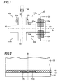
- Fig. 1 is a top view of a semiconductor wafer 10 during processing to manufacture the semiconductor device of the embodiment. Note that the front surface of the wafer 10 is shown in Fig. 1 with dice regions, and the back surface of the wafer 10 is attached to a supporting member (not shown in Fig. 1).
- semiconductor die regions 10a, 10b, 10c, and 10d and other semiconductor die regions which will be individual semiconductor dies by separating the semiconductor wafer 10, are disposed along dicing regions 60 perpendicularly crossing each other.
- First wirings 13a and 13b which are pads extending from circuits (not shown) formed on the semiconductor die regions are formed in the adjacent semiconductor die regions 10a and 10b, respectively, along the dicing region of the semiconductor wafer.
- a window 30 is formed so as to expose the first wirings 13a and 13b by selective etching, for example.
- This window 30 is an opening for connecting the first wirings 13a and 13b and second wirings to be formed in the semiconductor die regions 10a and 10b of the semiconductor wafer (wirings for connecting the first wirings and conductive terminals to be formed on the semiconductor wafer).
- semiconductor die regions 10c and 10d and the other semiconductor die regions also have the same structure as described above.
- alignment marks (51a, 51b) (52a, 52c) are respectively formed facing each other near the dicing regions 60 in corners of the semiconductor die regions 10a, 10b, 10c, and 10d, and the semiconductor die regions (not shown) of the semiconductor wafer, that is, near intersections of the crossing dicing regions 6, and near boundaries between the semiconductor die regions and the dicing regions 60.
- These alignment marks (51a, 51b) (52a, 52c) are protruded, for example, and used for alignment of a rotation blade on a predetermined cutting position in a cutting process for cutting the semiconductor wafer 10 or the glass substrate.
- the alignment of the rotation blade is performed by detecting the alignment marks (51a, 51b) (52a, 52c) by a recognition camera 80 for image recognition, calculating centerlines of the dicing regions 60 based on the detection result, and aligning the rotation blade on the centerlines.
- alignment marks (51a, 51b) (52a, 52c) are formed, having a following positional relationship, for example.
- the pair of alignment marks 51a and 51b is formed in the semiconductor die regions 10a and 10b respectively, facing each other near the dicing region 60 extending along a centerline 61 as a dicing line.
- the pair of alignment marks 52a and 52c is formed in the semiconductor die regions 10a and 10c respectively, facing each other near the dicing region 60 extending along a centerline 62. That is, the two pairs of alignment marks are formed near the intersection of the dicing regions 60.
- a pair of alignment marks is formed near each of the dicing regions 60 extending along the centerlines 61 and 62 near each of other intersections of the dicing regions 60, too, facing each other. That is, two pairs of alignment marks are formed near each of the intersections of the dicing regions 60.
- a pair of alignment marks is formed in each of the semiconductor die regions 10c and 10d, facing each other near the dicing region 60 extending along the centerline 61
- a pair of alignment marks is formed in each of the semiconductor die regions 10b and 10d, facing each other near the dicing region 60 extending along the centerline 62. This can improve accuracy of alignment mark recognition.
- a material of the alignment marks is not particularly limited as long as the marks can be detected by the recognition camera 80 for image recognition, it is preferable to use a material generally used in a manufacturing process of a semiconductor device.
- a material generally used in a manufacturing process of a semiconductor device can be the same material as the material of the first wiring and the wiring formed on the semiconductor wafer.
- the alignment marks can be protrusions or hollows formed by etching.
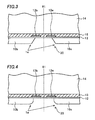
- Figs. 2 to 11 show cross-sectional views of the semiconductor die regions 10a and 10b and the dicing regions 60 along line X-X in the semiconductor wafer of Fig. 1.
- the other semiconductor die regions have the same structure as that shown in these cross-sectional views, too.
- the semiconductor wafer 10 formed with circuits (not shown) is prepared as shown in Fig. 2.
- the pair of first wirings 13a and 13b (wirings electrically connected with the circuits (not shown)) are formed on two sides of the centerline 61 (a center of the dicing region, i.e. a dicing line) respectively on the semiconductor wafer 10 with a first insulation film 12 interposed therebetween.
- a passivation film (not shown) made of a silicon oxide film or a silicon nitride film is formed on the semiconductor wafer 10 including the first wirings 13a and 13b.
- a glass substrate 14 as a supporting member is attached to a surface of the semiconductor wafer on the side formed with the first wirings 13a and 13b (referred to as a front surface of the semiconductor wafer 10, hereafter) with resin 15 (e.g. epoxy resin) interposed therebetween.
- the supporting member is not limited to the glass substrate, and a substrate or a tape made of metal or an organic material can be used as the supporting member, for example.
- the ground back surface of the semiconductor wafer 10 has small concave and convex portions which will be reflected in other layers or wirings to be formed on the semiconductor wafer afterward. Therefore, wet-etching can be performed to the ground back surface of the semiconductor wafer 10.
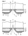
- a window 30 is formed in the semiconductor wafer 10 in a position corresponding to the first wirings 13a and 13b by selectively etching the back surface of the semiconductor wafer 10, serving as an opening exposing the first insulation film 12 formed on a part of the first wirings 13a and 13b.
- This window 30 is provided for connecting the first wirings 13a and 13b with second wirings to be formed on the back surface of the semiconductor wafer 10 afterward.
- the window 30 is not formed along the entire dicing region 60, that is, along all the centerline 61 but formed only in the position corresponding to the first wirings 13a and 13b, so that a contact area between the semiconductor wafer 10 and the glass substrate 14 is increased. This can reduce cracks or separation in the contact area, thereby preventing a yield decrease of the semiconductor device.
- Corners are formed in end portions 1a of the semiconductor wafer 10 in the window 30.
- the corners degrade step coverage of the other layers and wirings to be formed on the semiconductor wafer 10 afterward. Therefore, as shown in Fig. 4, wet-etching (or dip-etching) is performed to make the corners round.
- the alignment marks 51a, 51b, 52a, and 52c and other alignment marks (not shown) for aligning the rotation blade are formed near the intersections of the dicing regions 60 extending along the centerlines 61 and 62 on the back surface of the semiconductor wafer 10.
- a second insulation film 16 (e.g. an oxide film of 3 ⁇ m using silane as a base) is formed on the back surface of the semiconductor wafer 10.
- the alignment marks are covered with the second insulation film 16, since the alignment marks are protruded or hollowed in predetermined positions, the protrusions or hollows detectable by the recognition camera 80 are formed in the predetermined positions even on the second insulation film 16.
- the alignment marks are formed of a metal layer
- the alignment marks can be detected by the recognition camera 80 even when the alignment marks are covered with the second insulation film 16, since the second insulation film 16 forms the protrusions reflecting the metal layer.
- a resist film (not shown) is formed on the second insulation film 16, having an opening near the centerline 61 (near the centerline 62 in the other region formed with the first wiring) in the window 30.
- Etching is performed to the back surface of the semiconductor wafer 10 by using this resist film as a mask.
- a part of the second insulation film 16 and the first insulation film 12 is removed near the centerline 61 to expose a part of the first wirings 13a and 13b, as shown in Fig. 6.
- cushioning members 17 are formed in predetermined positions on the second insulation film 16. These cushioning members 17 are provided for absorbing stress applied to the conductive terminals to be formed in these positions afterward, and has a function of relaxing stress applied when the conductive terminals are attached to the printed circuit board.
- a metal layer for second wirings 18 is formed on the second insulation film 16 including on the cushioning members 17.
- the first wirings 13a and 13b are electrically connected with the second wirings 18.
- a resist film (not shown) is formed, being patterned to be opened in a region near the centerline 61 in the window 30 of the semiconductor wafer 10, that is, in a region except a region to be formed with the second wirings 18. Etching is performed to the metal layer with using this resist film as a mask, thereby forming the second wirings 18.
- the alignment marks 51a, 51b, 52a and 52c may be formed at this process step.
- this resist film is patterned so as to create a mask corresponding to the alignment marks, and the metal layer for the second wirings 18 is etched using this mask to create the alignment marks made of the metal layer.
- the alignment marks 51a, 51b, 52a and 52c may be formed by etching the layer that forms the base layer of the cushioning member 17.
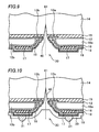
- a cut groove 40 having an inverse V shaped cross-section for example, and reaching a part of the glass substrate 14.
- the rotation blade used for the cutting must have such a width that the blade does not reach end portions of the first wirings 13a and 13b in the window 30.
- a shape of the cross-section of this cut groove 40 is not limited to the inverse V shape and can be other shapes (e.g. a rectangle).
- positions of the alignment marks are detected (recognized) by the recognition camera 80, and an accurate position of the centerline 61 is calculated based on the detection result. Then, the rotation blade is aligned on the calculated centerline 61 and the cutting is performed by moving the rotation blade along the centerline 61. Cutting along the centerline 62 is performed in a similar manner to this.
- the accurate positions of the centerlines 61 and 62 for cutting are determined based on the detection results of the positions of the pairs of alignment marks (51a, 51b) and (52a, 52c), respectively.
- each of the positions of the centerlines 61 and 62 is determined based on the detection result of an average value of the positions of the plural pairs of alignment marks on the dicing region 60. Then, a difference between the determined centerline and an original position of the rotation blade is calculated, and the position of the rotation blade is corrected by an amount of the difference.
- the alignment marks are recognized for aligning the rotation blade on the centerline 61 for forming the cut groove 40, and the position for the cutting is determined based on the recognition result.
- the position for the cutting can be determined based on a result of recognizing both end portions of the facing second wirings 18 electrically connected with the first wirings 13a and 13b, for example.
- the position for cutting depends on states of the end portions of the second wirings 18. Since the end portions of the second wirings 18 are formed on a bottom of the window 30, accuracy in patterning is not high, different from an ordinary patterning process. The end portions need have more accurately patterned shapes in order to be used as marks for positional recognition.
- the alignment marks of this invention are patterned at a flat portion as usual, and thus the accuracy is high, thereby having high reliability as marks for positional recognition.
- plating is performed to the second wirings 18 to form a plating film 19 made of, for example, Ni-Au.
- a protection film 20 is formed on the back surface of the semiconductor wafer 10 including in the cut groove 40.
- an organic resin is coated over the whole back surface of the semiconductor wafer 10 including the cut groove 40 by rotation coating of the organic resin.
- a resist film (not shown) is formed on the back surface of the semiconductor wafer 10, having openings in positions corresponding to the cushioning members 17.
- a part of the protection film 20 is removed by etching with using the resist film as a mask to form openings, and conductive terminals 21 are formed in the positions of the openings in the protection film 20.
- cutting is performed along the centerline 61 which is a center of the dicing region 60 to separate the semiconductor wafer 10 into individual semiconductor dies. Since the cut groove 40 is covered with the protection film 20, the cutting is performed to the glass substrate 14 and the protection layer 20 only. At this time, the rotation blade need have such a width that the blade does not reach the first wirings 13a and 13b and the resin 15 in the cut groove 40.
- the positions of the alignment marks are detected (recognized) by the recognition camera 80 before the cutting is performed, and the accurate position of the centerline 61 is calculated based on the detection result. Then, the rotation blade is aligned on the calculated centerline 61, and the cutting is performed with moving the rotation blade along the centerline 61. Cutting along the centerline 62 is performed in a similar manner to this.
- the alignment of the rotation blade is performed, for example, by detecting the positions of the end portions 8a and 8b of the second wirings 18a and 18b exposed in the cut groove 40 by the recognition camera 80, calculating the center of the dicing region 60, that is, the centerline 61 based on the detection result, and aligning the rotation blade on the calculated centerline 61, as shown in Fig. 12 which is a plan view of an inside of the window 30 formed in the semiconductor wafer 10 seen from an upper side thereof.
- the end portions 8a and 8b of the second wirings 18a and 18b often have a fracture surface (surface having concave and convex portions) formed in the process for the formation, so that it is difficult to detect the positions accurately. This causes a problem that the position of the centerline 61 is calculated inaccurately based on the positions of the end portions 8a and 8b.
- the semiconductor device manufacturing method of the embodiment using the alignment marks in the cutting processes does not depend on the positions of the end portions 8a and 8b of the second wirings 18a and 18b. Therefore, the alignment of the rotation blade can be performed more accurately, compared with the method employing the end portions 8a and 8b for the detection. Accordingly, the cutting accuracy in the semiconductor wafer can be improved.
- the same alignment marks can be commonly used for a plurality of different cutting processes performed to the dicing region 60, that is, for both the formation of the cut groove 40 and the separation of the semiconductor wafer 10. Accordingly, in a case where a plurality of cutting processes is needed for the dicing region 60 as in the manufacturing method of the semiconductor device attached with a supporting member in the described embodiment, a positional shift in alignment of the rotation blade can be minimized. This can improve the cutting accuracy in the semiconductor wafer 10.
- the semiconductor device attached with the supporting member can be realized by using one sheet of a glass substrate while the yield decrease is prevented.
- An increase of a thickness and a manufacturing cost of the semiconductor device can be minimized, compared with a case of using two sheets of glass substrates.
- the alignment of the rotation blade using the alignment marks is applied to the semiconductor device attached with one sheet of glass substrate in this embodiment, modifications are possible. That is, the invention is applicable to semiconductor devices having other structures such as a semiconductor device having two sheets of glass substrates attached to its two sides respectively.
Landscapes
- Health & Medical Sciences (AREA)
- Engineering & Computer Science (AREA)
- Anesthesiology (AREA)
- Biomedical Technology (AREA)
- Heart & Thoracic Surgery (AREA)
- Hematology (AREA)
- Life Sciences & Earth Sciences (AREA)
- Animal Behavior & Ethology (AREA)
- General Health & Medical Sciences (AREA)
- Public Health (AREA)
- Veterinary Medicine (AREA)
- Dicing (AREA)
Abstract

Description
Fig. 13B is a perspective view of the BGA type semiconductor device on its back surface.
Claims (12)
- A method of manufacturing a semiconductor device, comprising:providing a semiconductor wafer (10) comprising a layer disposed on a front surface of the semiconductor wafer, a first electrode pad (13a) and a second electrode pad (13b) that are formed on the front surface, and a supporting member (14) attached to the front surface;forming on a back surface of the semiconductor wafer a first alignment mark (51a) and a second alignment mark (51b);detecting positions of the first and second alignment marks (51a,b);calculating a middle position (61) of the positions of the first and second alignment marks (51a,b);placing a blade at the calculated middle position (61) on a side of the semiconductor wafer (10) corresponding to the back surface; andcutting using the aligned blade the layer (15) disposed on the front surface between the first and second electrode pads (13a,b) and along a predetermined direction so that the blade reaches the semiconductor wafer (10).
- The method of claim 1, wherein the predetermined direction is a direction normal to a direction connecting the first and second alignment marks (13a,b).
- The method of claim 1 or 2, wherein the detecting is performed using a recognition camera (80).
- The method according to any of claims 1 to 3, further comprising etching the semiconductor wafer (10) from the back surface to expose the first and second electrode pads (13a,b).
- The method according to any of claims 1 to 4, wherein the first and second alignment marks (51a,b) are formed of a material used in a manufacturing process of the semiconductor device.
- The method according to any of claims 1 to 5, wherein the first and second alignment marks (51a,b) are dents formed by etching.
- The method according to any of claims 1 to 6, further comprising another detecting of the positions of the first and second alignment marks (51a,c), another calculating of the middle position (61), placing a blade at the calculated middle position (61), and cutting the supporting member (14) at the calculated middle position (61) along the predetermined direction so as to form individual semiconductor dies.
- The method of claim 7, wherein the first and second alignment marks (51a,b) are formed of a material used in a manufacturing process of the semiconductor device.
- The method of claim 7, wherein the first and second alignment marks (51a,b) are dents formed by etching.
- A semiconductor device comprising:a semiconductor die (10);a pad electrode (13a,b) disposed on a front surface of the semiconductor die (10);a supporting member (14) attached to the front surface; andan alignment mark (51a,b) disposed on a back surface of the semiconductor die (10).
- The semiconductor device of claim 10, wherein the alignment mark (51a,b) is formed of a material used in a manufacturing process of the semiconductor device (10).
- The semiconductor device of claim 11, wherein the alignment mark (51a,b) is a dent formed by etching.
Applications Claiming Priority (2)
| Application Number | Priority Date | Filing Date | Title |
|---|---|---|---|
| JP2004062323 | 2004-03-05 | ||
| JP2004062323A JP4753170B2 (en) | 2004-03-05 | 2004-03-05 | Semiconductor device and manufacturing method thereof |
Publications (2)
| Publication Number | Publication Date |
|---|---|
| EP1575086A2 true EP1575086A2 (en) | 2005-09-14 |
| EP1575086A3 EP1575086A3 (en) | 2006-06-14 |
Family
ID=34824512
Family Applications (1)
| Application Number | Title | Priority Date | Filing Date |
|---|---|---|---|
| EP05004918A Withdrawn EP1575086A3 (en) | 2004-03-05 | 2005-03-07 | Semiconductor device and manufacturing method of the same, including a dicing step |
Country Status (7)
| Country | Link |
|---|---|
| US (1) | US7456083B2 (en) |
| EP (1) | EP1575086A3 (en) |
| JP (1) | JP4753170B2 (en) |
| KR (1) | KR100682003B1 (en) |
| CN (1) | CN100446187C (en) |
| SG (1) | SG114787A1 (en) |
| TW (1) | TWI288956B (en) |
Cited By (1)
| Publication number | Priority date | Publication date | Assignee | Title |
|---|---|---|---|---|
| WO2009007930A3 (en) * | 2007-07-12 | 2009-04-30 | Nxp Bv | Integrated circuits on a wafer and method for separating integrated circuits on a wafer |
Families Citing this family (42)
| Publication number | Priority date | Publication date | Assignee | Title |
|---|---|---|---|---|
| TWI232560B (en) * | 2002-04-23 | 2005-05-11 | Sanyo Electric Co | Semiconductor device and its manufacture |
| TWI229435B (en) * | 2002-06-18 | 2005-03-11 | Sanyo Electric Co | Manufacture of semiconductor device |
| TWI227550B (en) * | 2002-10-30 | 2005-02-01 | Sanyo Electric Co | Semiconductor device manufacturing method |
| JP4401181B2 (en) * | 2003-08-06 | 2010-01-20 | 三洋電機株式会社 | Semiconductor device and manufacturing method thereof |
| JP3962713B2 (en) * | 2003-09-30 | 2007-08-22 | キヤノン株式会社 | Alignment mark forming method and substrate on which device is formed |
| JP4322181B2 (en) * | 2004-07-29 | 2009-08-26 | 三洋電機株式会社 | Manufacturing method of semiconductor device |
| US20060258051A1 (en) * | 2005-05-10 | 2006-11-16 | Texas Instruments Incorporated | Method and system for solder die attach |
| KR100652435B1 (en) * | 2005-10-07 | 2006-12-01 | 삼성전자주식회사 | Method of attaching wafers and dies to wafers with display means for distinguishing the position of the first die |
| US8153464B2 (en) * | 2005-10-18 | 2012-04-10 | International Rectifier Corporation | Wafer singulation process |
| TWI324800B (en) * | 2005-12-28 | 2010-05-11 | Sanyo Electric Co | Method for manufacturing semiconductor device |
| TW200737506A (en) * | 2006-03-07 | 2007-10-01 | Sanyo Electric Co | Semiconductor device and manufacturing method of the same |
| JP2007329153A (en) * | 2006-06-06 | 2007-12-20 | Fujitsu Ltd | Device manufacturing method, dicing method, and dicing apparatus |
| CN100524719C (en) * | 2006-08-03 | 2009-08-05 | 南茂科技股份有限公司 | Array packaging substrate and method for judging cutting mode of packaging body array |
| US8102039B2 (en) | 2006-08-11 | 2012-01-24 | Sanyo Semiconductor Co., Ltd. | Semiconductor device and manufacturing method thereof |
| JP5076407B2 (en) * | 2006-09-05 | 2012-11-21 | ミツミ電機株式会社 | Semiconductor device and manufacturing method thereof |
| KR100784388B1 (en) * | 2006-11-14 | 2007-12-11 | 삼성전자주식회사 | Semiconductor Package and Manufacturing Method |
| JP5010247B2 (en) | 2006-11-20 | 2012-08-29 | オンセミコンダクター・トレーディング・リミテッド | Semiconductor device and manufacturing method thereof |
| US7569409B2 (en) * | 2007-01-04 | 2009-08-04 | Visera Technologies Company Limited | Isolation structures for CMOS image sensor chip scale packages |
| US7679167B2 (en) * | 2007-01-08 | 2010-03-16 | Visera Technologies Company, Limited | Electronic assembly for image sensor device and fabrication method thereof |
| JP2008294405A (en) * | 2007-04-25 | 2008-12-04 | Sanyo Electric Co Ltd | Semiconductor device and manufacturing method thereof |
| JP2008288285A (en) * | 2007-05-15 | 2008-11-27 | Sharp Corp | LAMINATED SUBSTRATE CUTTING METHOD, SEMICONDUCTOR DEVICE MANUFACTURING METHOD, SEMICONDUCTOR DEVICE, LIGHT EMITTING DEVICE, AND BACKLIGHT DEVICE |
| DE102007030284B4 (en) * | 2007-06-29 | 2009-12-31 | Schott Ag | Process for packaging semiconductor devices and intermediate product produced by the process |
| US8338267B2 (en) * | 2007-07-11 | 2012-12-25 | Sematech, Inc. | Systems and methods for vertically integrating semiconductor devices |
| TWI375321B (en) * | 2007-08-24 | 2012-10-21 | Xintec Inc | Electronic device wafer level scale packages and fabrication methods thereof |
| CN101950729B (en) * | 2007-09-05 | 2012-09-26 | 精材科技股份有限公司 | Wafer-level packaging of electronic components and manufacturing method thereof |
| JP2010103300A (en) * | 2008-10-23 | 2010-05-06 | Sanyo Electric Co Ltd | Semiconductor device, and method of manufacturing the same |
| US8289388B2 (en) * | 2009-05-14 | 2012-10-16 | Asm Assembly Automation Ltd | Alignment method for singulation system |
| CN102800656B (en) * | 2011-05-20 | 2015-11-25 | 精材科技股份有限公司 | Chip package, method for forming chip package, and packaged wafer |
| DE102011112659B4 (en) * | 2011-09-06 | 2022-01-27 | Vishay Semiconductor Gmbh | Surface mount electronic component |
| JP6096442B2 (en) * | 2012-09-10 | 2017-03-15 | ラピスセミコンダクタ株式会社 | Semiconductor device and manufacturing method of semiconductor device |
| JP6193665B2 (en) * | 2013-07-26 | 2017-09-06 | ルネサスエレクトロニクス株式会社 | Manufacturing method of semiconductor device |
| JP6257291B2 (en) * | 2013-12-04 | 2018-01-10 | 株式会社ディスコ | Processing method of package substrate |
| CN104977745B (en) * | 2015-06-24 | 2018-05-25 | 武汉华星光电技术有限公司 | Substrate for liquid crystal display panel and liquid crystal display panel cutting method |
| JP2017053999A (en) * | 2015-09-09 | 2017-03-16 | 株式会社東芝 | Semiconductor device and inspection pattern arrangement method |
| JP6607639B2 (en) * | 2015-12-24 | 2019-11-20 | 株式会社ディスコ | Wafer processing method |
| US10163954B2 (en) * | 2016-04-11 | 2018-12-25 | Omnivision Technologies, Inc. | Trenched device wafer, stepped-sidewall device die, and associated method |
| JP2019054172A (en) * | 2017-09-15 | 2019-04-04 | 東芝メモリ株式会社 | Semiconductor device |
| JP7075652B2 (en) * | 2017-12-28 | 2022-05-26 | 三星ダイヤモンド工業株式会社 | Scribe device and scribe method |
| DE102019204457B4 (en) * | 2019-03-29 | 2024-01-25 | Disco Corporation | Substrate processing methods |
| CN110549351B (en) * | 2019-09-19 | 2020-10-30 | 中国科学院合肥物质科学研究院 | Material oxide layer polishing robot control system and control method thereof |
| CN111128966A (en) * | 2019-12-25 | 2020-05-08 | 华天科技(昆山)电子有限公司 | Alignment structure and package cutting method |
| CN117672886A (en) * | 2022-08-25 | 2024-03-08 | 群创光电股份有限公司 | Manufacturing method of electronic device |
Family Cites Families (20)
| Publication number | Priority date | Publication date | Assignee | Title |
|---|---|---|---|---|
| JPS6030314A (en) * | 1983-07-08 | 1985-02-15 | 富士通株式会社 | Dicing device |
| JPH04177715A (en) * | 1990-11-10 | 1992-06-24 | Fujitsu Ltd | Semiconductor device |
| JP2666761B2 (en) | 1995-03-28 | 1997-10-22 | 日本電気株式会社 | Semiconductor wafer |
| US5777392A (en) * | 1995-03-28 | 1998-07-07 | Nec Corporation | Semiconductor device having improved alignment marks |
| KR970008386A (en) * | 1995-07-07 | 1997-02-24 | 하라 세이지 | A method of dividing a substrate and a dividing device |
| IL123207A0 (en) * | 1998-02-06 | 1998-09-24 | Shellcase Ltd | Integrated circuit device |
| US6271102B1 (en) * | 1998-02-27 | 2001-08-07 | International Business Machines Corporation | Method and system for dicing wafers, and semiconductor structures incorporating the products thereof |
| JP3065309B1 (en) * | 1999-03-11 | 2000-07-17 | 沖電気工業株式会社 | Method for manufacturing semiconductor device |
| WO2001009927A1 (en) * | 1999-07-28 | 2001-02-08 | Infineon Technologies North America Corp. | Semiconductor structures and manufacturing methods |
| US6309943B1 (en) * | 2000-04-25 | 2001-10-30 | Amkor Technology, Inc. | Precision marking and singulation method |
| US6579738B2 (en) * | 2000-12-15 | 2003-06-17 | Micron Technology, Inc. | Method of alignment for buried structures formed by surface transformation of empty spaces in solid state materials |
| US6869861B1 (en) * | 2001-03-08 | 2005-03-22 | Amkor Technology, Inc. | Back-side wafer singulation method |
| JP3603828B2 (en) * | 2001-05-28 | 2004-12-22 | 富士ゼロックス株式会社 | Ink jet recording head, method of manufacturing the same, and ink jet recording apparatus |
| JP3872319B2 (en) * | 2001-08-21 | 2007-01-24 | 沖電気工業株式会社 | Semiconductor device and manufacturing method thereof |
| JP2003100666A (en) * | 2001-09-26 | 2003-04-04 | Toshiba Corp | Method for manufacturing semiconductor device |
| JP3877700B2 (en) * | 2002-04-23 | 2007-02-07 | 三洋電機株式会社 | Semiconductor device and manufacturing method thereof |
| JP2004006820A (en) * | 2002-04-23 | 2004-01-08 | Sanyo Electric Co Ltd | Semiconductor device and manufacturing method thereof |
| JP2003347476A (en) * | 2002-05-22 | 2003-12-05 | Sanyo Electric Co Ltd | Semiconductor integrated device and method of manufacturing the same |
| CN2552163Y (en) * | 2002-05-23 | 2003-05-21 | 立卫科技股份有限公司 | The structure of the electroplating line at the identification point of package cutting |
| JP3796202B2 (en) * | 2002-07-05 | 2006-07-12 | 三洋電機株式会社 | Manufacturing method of semiconductor integrated device |
-
2004
- 2004-03-05 JP JP2004062323A patent/JP4753170B2/en not_active Expired - Fee Related
-
2005
- 2005-02-18 TW TW094104769A patent/TWI288956B/en not_active IP Right Cessation
- 2005-03-02 US US11/069,061 patent/US7456083B2/en not_active Expired - Lifetime
- 2005-03-04 CN CNB2005100530225A patent/CN100446187C/en not_active Expired - Fee Related
- 2005-03-04 KR KR1020050018007A patent/KR100682003B1/en not_active Expired - Fee Related
- 2005-03-05 SG SG200501359A patent/SG114787A1/en unknown
- 2005-03-07 EP EP05004918A patent/EP1575086A3/en not_active Withdrawn
Cited By (2)
| Publication number | Priority date | Publication date | Assignee | Title |
|---|---|---|---|---|
| WO2009007930A3 (en) * | 2007-07-12 | 2009-04-30 | Nxp Bv | Integrated circuits on a wafer and method for separating integrated circuits on a wafer |
| US8415769B2 (en) | 2007-07-12 | 2013-04-09 | Nxp B.V. | Integrated circuits on a wafer and method for separating integrated circuits on a wafer |
Also Published As
| Publication number | Publication date |
|---|---|
| JP2005252078A (en) | 2005-09-15 |
| KR20060043788A (en) | 2006-05-15 |
| US20050208735A1 (en) | 2005-09-22 |
| SG114787A1 (en) | 2005-09-28 |
| CN1664991A (en) | 2005-09-07 |
| CN100446187C (en) | 2008-12-24 |
| JP4753170B2 (en) | 2011-08-24 |
| EP1575086A3 (en) | 2006-06-14 |
| KR100682003B1 (en) | 2007-02-15 |
| US7456083B2 (en) | 2008-11-25 |
| TW200535941A (en) | 2005-11-01 |
| TWI288956B (en) | 2007-10-21 |
Similar Documents
| Publication | Publication Date | Title |
|---|---|---|
| US7456083B2 (en) | Semiconductor device and manufacturing method of the same | |
| US7045908B2 (en) | Semiconductor device and method for manufacturing the same | |
| CN100367451C (en) | Semiconductor device and method for manufacturing the same | |
| EP1416529B1 (en) | Manufacturing method of semiconductor device | |
| JP3739375B2 (en) | Semiconductor device and manufacturing method thereof | |
| US7413931B2 (en) | Semiconductor device manufacturing method | |
| US6303470B1 (en) | Semiconductor wafer and method for manufacturing semiconductor devices | |
| US20050019982A1 (en) | Semiconductor package having semiconductor constructing body and method of manufacturing the same | |
| US7759808B2 (en) | Semiconductor substrate including first and second recognition marks and method for manufacturing semiconductor device | |
| KR20030084707A (en) | Semiconductor device and manufacturing method thereof | |
| US7241679B2 (en) | Method of manufacturing semiconductor device | |
| US6077757A (en) | Method of forming chip semiconductor devices | |
| EP1748485A2 (en) | Semiconductor device and manufacturing method of the same | |
| EP1686622A2 (en) | Semiconductor device and manufacturing method of the same | |
| US7557017B2 (en) | Method of manufacturing semiconductor device with two-step etching of layer | |
| US7030508B2 (en) | Substrate for semiconductor package and wire bonding method using thereof | |
| JP2010199625A (en) | Semiconductor device, and method of manufacturing the same | |
| US20050266609A1 (en) | Method of fabricating a built-in chip type substrate | |
| JP3877700B2 (en) | Semiconductor device and manufacturing method thereof | |
| US20040238973A1 (en) | Semiconductor device having alignment post electrode and method of manufacturing the same | |
| JP2010016395A (en) | Manufacturing method for semiconductor device | |
| JP3988679B2 (en) | Semiconductor substrate | |
| US8796869B2 (en) | Semiconductor device and method of manufacturing the same | |
| JP4401330B2 (en) | Semiconductor device and manufacturing method thereof | |
| JP2003188333A (en) | Semiconductor device and method of manufacturing the same |
Legal Events
| Date | Code | Title | Description |
|---|---|---|---|
| PUAI | Public reference made under article 153(3) epc to a published international application that has entered the european phase |
Free format text: ORIGINAL CODE: 0009012 |
|
| AK | Designated contracting states |
Kind code of ref document: A2 Designated state(s): AT BE BG CH CY CZ DE DK EE ES FI FR GB GR HU IE IS IT LI LT LU MC NL PL PT RO SE SI SK TR |
|
| AX | Request for extension of the european patent |
Extension state: AL BA HR LV MK YU |
|
| PUAL | Search report despatched |
Free format text: ORIGINAL CODE: 0009013 |
|
| AK | Designated contracting states |
Kind code of ref document: A3 Designated state(s): AT BE BG CH CY CZ DE DK EE ES FI FR GB GR HU IE IS IT LI LT LU MC NL PL PT RO SE SI SK TR |
|
| AX | Request for extension of the european patent |
Extension state: AL BA HR LV MK YU |
|
| 17P | Request for examination filed |
Effective date: 20061213 |
|
| AKX | Designation fees paid |
Designated state(s): DE FI FR GB |
|
| 17Q | First examination report despatched |
Effective date: 20080801 |
|
| STAA | Information on the status of an ep patent application or granted ep patent |
Free format text: STATUS: THE APPLICATION HAS BEEN WITHDRAWN |
|
| 18W | Application withdrawn |
Effective date: 20090710 |