EP1575080B1 - Light-emitting device and use thereof - Google Patents
Light-emitting device and use thereof Download PDFInfo
- Publication number
- EP1575080B1 EP1575080B1 EP04030244A EP04030244A EP1575080B1 EP 1575080 B1 EP1575080 B1 EP 1575080B1 EP 04030244 A EP04030244 A EP 04030244A EP 04030244 A EP04030244 A EP 04030244A EP 1575080 B1 EP1575080 B1 EP 1575080B1
- Authority
- EP
- European Patent Office
- Prior art keywords
- light
- host element
- filiform
- emission
- source
- Prior art date
- Legal status (The legal status is an assumption and is not a legal conclusion. Google has not performed a legal analysis and makes no representation as to the accuracy of the status listed.)
- Expired - Lifetime
Links
- 239000004038 photonic crystal Substances 0.000 claims abstract description 13
- 229910052721 tungsten Inorganic materials 0.000 claims description 8
- 239000010937 tungsten Substances 0.000 claims description 8
- 230000000737 periodic effect Effects 0.000 claims description 7
- WFKWXMTUELFFGS-UHFFFAOYSA-N tungsten Chemical compound [W] WFKWXMTUELFFGS-UHFFFAOYSA-N 0.000 claims description 7
- 238000004519 manufacturing process Methods 0.000 claims description 3
- 239000000109 continuous material Substances 0.000 claims description 2
- 239000012780 transparent material Substances 0.000 claims description 2
- 230000005855 radiation Effects 0.000 abstract description 14
- 230000002269 spontaneous effect Effects 0.000 description 7
- 238000000034 method Methods 0.000 description 5
- 230000003287 optical effect Effects 0.000 description 5
- 230000003321 amplification Effects 0.000 description 4
- 239000013078 crystal Substances 0.000 description 4
- 239000000463 material Substances 0.000 description 4
- 238000003199 nucleic acid amplification method Methods 0.000 description 4
- 239000004065 semiconductor Substances 0.000 description 4
- 230000015572 biosynthetic process Effects 0.000 description 3
- 230000005670 electromagnetic radiation Effects 0.000 description 3
- 230000003595 spectral effect Effects 0.000 description 3
- GWEVSGVZZGPLCZ-UHFFFAOYSA-N Titan oxide Chemical compound O=[Ti]=O GWEVSGVZZGPLCZ-UHFFFAOYSA-N 0.000 description 2
- 230000005540 biological transmission Effects 0.000 description 2
- 238000010276 construction Methods 0.000 description 2
- 230000008878 coupling Effects 0.000 description 2
- 238000010168 coupling process Methods 0.000 description 2
- 238000005859 coupling reaction Methods 0.000 description 2
- 239000011521 glass Substances 0.000 description 2
- 239000011261 inert gas Substances 0.000 description 2
- 230000003993 interaction Effects 0.000 description 2
- 239000011159 matrix material Substances 0.000 description 2
- 230000008569 process Effects 0.000 description 2
- 230000009471 action Effects 0.000 description 1
- PNEYBMLMFCGWSK-UHFFFAOYSA-N aluminium oxide Inorganic materials [O-2].[O-2].[O-2].[Al+3].[Al+3] PNEYBMLMFCGWSK-UHFFFAOYSA-N 0.000 description 1
- 230000002547 anomalous effect Effects 0.000 description 1
- 238000003486 chemical etching Methods 0.000 description 1
- 239000003989 dielectric material Substances 0.000 description 1
- 239000002019 doping agent Substances 0.000 description 1
- 239000012535 impurity Substances 0.000 description 1
- 238000002844 melting Methods 0.000 description 1
- 230000008018 melting Effects 0.000 description 1
- 229910052751 metal Inorganic materials 0.000 description 1
- 239000002184 metal Substances 0.000 description 1
- 210000003632 microfilament Anatomy 0.000 description 1
- 238000001393 microlithography Methods 0.000 description 1
- 239000000203 mixture Substances 0.000 description 1
- 238000005329 nanolithography Methods 0.000 description 1
- 229920000620 organic polymer Polymers 0.000 description 1
- 238000000206 photolithography Methods 0.000 description 1
- 239000000843 powder Substances 0.000 description 1
- 229910052710 silicon Inorganic materials 0.000 description 1
- 239000010703 silicon Substances 0.000 description 1
- 150000003384 small molecules Chemical class 0.000 description 1
- 150000003657 tungsten Chemical class 0.000 description 1
Images

Classifications
-
- H—ELECTRICITY
- H01—ELECTRIC ELEMENTS
- H01K—ELECTRIC INCANDESCENT LAMPS
- H01K1/00—Details
- H01K1/02—Incandescent bodies
-
- H—ELECTRICITY
- H01—ELECTRIC ELEMENTS
- H01K—ELECTRIC INCANDESCENT LAMPS
- H01K5/00—Lamps for general lighting
-
- H—ELECTRICITY
- H01—ELECTRIC ELEMENTS
- H01K—ELECTRIC INCANDESCENT LAMPS
- H01K7/00—Lamps for purposes other than general lighting
Definitions
- the present invention relates to a light-emitting device, comprising a substantially filiform light source, which can be activated via passage of electric current.
- the electric current traverses a light source constituted by a filament made of tungsten, housed in a glass bulb in which a vacuum has been formed or in which an atmosphere of inert gases is present, and renders said filament incandescent.
- the emission of electromagnetic radiation thus obtained follows, to a first approximation, the so-called black-body distribution corresponding to the temperature T of the filament (in general, approximately 2700K).
- the emission of electromagnetic radiation in the region of visible light (380-780 nm), as represented by the curve A in the attached Figure 1 is just one portion of the total emission curve.
- US-A-2003/071564 upon which the preamble of claim 1 is based, discloses a light emitting device which emits visible light through heat radiation of a tungsten filament.
- Photonic crystal structures in each of which Ag spheres are arranged in a TiO2 film, are provided around the filament. Radiation of infrared light from the filament is suppressed, whereas radiation of visible light is enhanced.
- WO-A-03/058676 discloses a three-dimensional structure in the form of filament for an incandescent lamp.
- This filament is formed by a plurality of tungsten microfilaments having micrometric and/or nanometric dimensions, which are arranged so as to form a photonic crystal structure.
- the described arrangement makes it possible to prevent propagation and spontaneous emission of IR radiation of specific wavelenghts e allows at the same time propagation and spontaneous emission of visible radiation.
- US-A-5,152,870 discloses a method for fabricating incandescent lamp filaments having surface features of submicron-to-micron sized cross sections which increase the radiative efficiency of the filament.
- the desired surface features are formed on the filament by a process that includes stenciling through the selected pattern.
- JP-A-04 349338 discloses a filament for light bulb including a coil made of high melting point metal surrounded by a body having an ultra-fine gap.
- the gap of the surrounding body is selected to control emission of radiation of specified wavelength. Transmission of visible light is allowed through the diffraction action of the fine gap, while radiation of the other wavelength range is restricted.
- the present invention is mainly aimed at providing a device of the type indicated above that enables a selectivity and above all an amplification of the electromagnetic radiation of the optical region, or of a specific chromatic band, at the expense of the infrared region, as highlighted for example by the curve B of Figure 1 .
- Figure 2 represents a light-emitting device according to the invention.
- the device has the shape of an ordinary light bulb, designated as a whole by 1, but this shape is to be understood herein as being chosen purely by way of example.
- the light bulb 1 comprises a glass bulb, designated by 2, which is filled with a mixture of inert gases, or else in which a vacuum is created, and a bulb base, designated by 3.
- a glass bulb designated by 2
- a bulb base designated by 3.
- the contacts 4 and 5 are electrically connected to respective terminals formed in a known way in the bulb base 3. Connection of the bulb base 3 to a respective bulb socket enables connection of the light bulb 1 to the electrical-supply circuit.
- the idea underlying the present invention is that of integrating or englobing a substantially filiform light source, which can be excited or brought electrically to incandescence, in a host element structured according to nanometric or sub-micrometric dimensions in order to obtain a desired spectral selectivity of emission, with an amplification of the radiation emitted in the visible region at the expense of the infrared portion.
- the emitter element may be made of a continuous material, for example in the form of a tungsten filament, or else of a cluster of one or more molecules in contact of a semiconductor type, or of a metallic type, or in general of an organic-polymer type with a complex chain or with small molecules.
- the host element which englobes the emitter element may be nano-structured via removal of material so as to form micro-cavities.
- the light-emitting device proves more efficient since the infrared emission can be inhibited and its energy transferred into the optical region. Furthermore, for this reason the temperature of the light-emitter element is lower than that of traditional light bulbs and light sources.
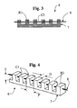
- Figures 3 and 4 illustrate a portion of a light source or emitter 6 according to the invention, which comprises a host element 7, integrated in which is a filament, designated by 8, which can be brought to incandescence and which may be made, for example, of tungsten or powders of tungsten.
- the host element 7 is structured according to micrometric or nanometric dimensions, so as to present an orderly and periodic series of micro-cavities C1, intercalated by full portions or projections R1 of the same element.
- the filament 8 Integrated in the host element 7 is the filament 8 in such a way that the latter will pass, in the direction of its length, both through the cavities C1 and through the projections R1.
- the host element 7 is structured in the form of a one-dimensional photonic crystal, namely, a crystal provided with projections R1 and cavities C1 that are periodic in just one direction on the surface of the element itself.
- h is the depth of the cavities C1 (which corresponds to the height of the projections R1)
- D is the width of the projections R1
- P is the period of the grating
- the filling factor of the grating R is defined as the ratio D/P.
- the electrons that move in a semiconductor crystal are affected by a periodic potential generated by the interaction with the nuclei of the atoms that constitute the crystal itself. This interaction results in the formation of a series of allowed energy bands, separated by forbidden energy bands (band gaps).
- photonic crystals which are generally constituted by bodies made of transparent dielectric material defining an orderly series of micro-cavities in which there is present air or some other means having an index of refraction very different from that of the host matrix.
- the contrast between the indices of refraction causes confinement of photons with given wavelengths within the cavities of the photonic crystal.
- the confinement to which the photons (or the electromagnetic waves) are subject on account of the contrast between the indices of refraction of the porous matrix and of the cavities results in the formation of regions of allowed energies, separated by regions of forbidden energies. The latter are referred to as photonic band gaps (PBGs). From this fact there follow the two fundamental properties of photonic crystals:
- micro-cavities C1 within which the emission of light produced by the filament 8 brought to incandescence is at least in part confined in such a way that the frequencies that cannot propagate as a result of the band gap are reflected.
- the surfaces of the micro-cavities C1 hence operate as mirrors for the wavelengths belonging to the photonic band gap.
- the grating can be made so as to determine a photonic band gap that will prevent spontaneous emission and propagation of infrared radiation, and at the same time enable the peak of emission in a desired area in the 380-780-nm range to be obtained in order to produce, for instance, a light visible as blue, green, red, etc.
- the host element 7 can be made using any transparent material, suitable for being surface nano-structured and for withstanding the temperatures developed by the incandescence of the filament 8.
- the techniques of production of the emitter element 6 provided with periodic structure of micro-cavities C1 may be based upon nano- and micro-lithography, nano- and micro-photolithography, anodic electrochemical processes, chemical etching, etc., i.e., techniques already known in the production of photonic crystals (alumina, silicon, and so on).
- the two ends of the element 8 will be connected to appropriate electrical terminals for application of a potential difference.
- the filament 8 is electrically connected to the contacts 4 and 5.
- the device according to the invention enables the desired chromatic selectivity of the light emission to be obtained and, above all, its amplification in the visible region.
- the most efficient results, in the case of the embodiment represented in Figures 3, 4 is obtained by causing the filament 8 to extend through approximately half of the depth of the cavities C1. With this geometry, coupling between the density of the modes present in the cavity (maximum peak at the centre of the cavity) and the emitting element is optimized.
- the invention enables amplification of radiation emitted in the visible region at the expense of the infrared portion, via the construction of elements 6 that englobe the filament 8 and that are nano-structured through removal of material, as in Figures 3-4 .
- the device thus obtained is more efficient, in so far as the infrared emission is inhibited, and its energy is transferred into the visible range, as is evident from Figure 1 . For this reason, moreover, the temperature of the filament 8 is lower than that of traditional light bulbs.
- the accuracy with which the aforesaid nanometric structures can be obtained gives rise to a further property, namely, chromatic selectivity.
- chromatic selectivity In the visible region there can then further be selected the emission lines, once again exploiting the principle used for eliminating the infrared radiation, for example to provide monochromatic sources of the LED type.
- the emitter 6 may be obtained in the desired length and, obviously, may be used in devices other than light bulbs.
- emitters structured according to the invention may advantageously be used for the formation of pixels with the R, G and B components of luminescent devices or displays.
- the emitters structured according to the invention are, like optical fibres, characterized by a considerable flexibility, so that they can be arranged as desired to form complex patterns.
- the photonic-crystal structure defined in the host element 7 is of the one-dimensional type, but it is clear that in possible variant embodiments of the invention the grating may have more dimensions, for example be two-dimensional, i.e., with periodic cavities/projections in two orthogonal directions on the surface of the element 7.
- the electrically-excited source 8 may be made in full filiform forms, integrated in a structure 7 of the photonic-crystal type.
Landscapes
- Light Guides In General And Applications Therefor (AREA)
- Non-Portable Lighting Devices Or Systems Thereof (AREA)
- Luminescent Compositions (AREA)
- Surgical Instruments (AREA)
- Led Device Packages (AREA)
- Led Devices (AREA)
- Pinball Game Machines (AREA)
- Devices For Indicating Variable Information By Combining Individual Elements (AREA)
- Optical Modulation, Optical Deflection, Nonlinear Optics, Optical Demodulation, Optical Logic Elements (AREA)
Applications Claiming Priority (2)
| Application Number | Priority Date | Filing Date | Title |
|---|---|---|---|
| ITTO20040018 | 2004-01-16 | ||
| IT000018A ITTO20040018A1 (it) | 2004-01-16 | 2004-01-16 | Dispositivo emettitore di luce |
Publications (3)
| Publication Number | Publication Date |
|---|---|
| EP1575080A2 EP1575080A2 (en) | 2005-09-14 |
| EP1575080A3 EP1575080A3 (en) | 2007-08-15 |
| EP1575080B1 true EP1575080B1 (en) | 2011-04-13 |
Family
ID=34803710
Family Applications (1)
| Application Number | Title | Priority Date | Filing Date |
|---|---|---|---|
| EP04030244A Expired - Lifetime EP1575080B1 (en) | 2004-01-16 | 2004-12-21 | Light-emitting device and use thereof |
Country Status (7)
| Country | Link |
|---|---|
| US (1) | US7498730B2 (it) |
| EP (1) | EP1575080B1 (it) |
| CN (1) | CN1641829A (it) |
| AT (1) | ATE505810T1 (it) |
| DE (1) | DE602004032209D1 (it) |
| IT (1) | ITTO20040018A1 (it) |
| RU (1) | RU2005100868A (it) |
Families Citing this family (21)
| Publication number | Priority date | Publication date | Assignee | Title |
|---|---|---|---|---|
| US5876621A (en) * | 1997-09-30 | 1999-03-02 | Sapienza; Richard | Environmentally benign anti-icing or deicing fluids |
| US7777235B2 (en) | 2003-05-05 | 2010-08-17 | Lighting Science Group Corporation | Light emitting diodes with improved light collimation |
| US7528421B2 (en) * | 2003-05-05 | 2009-05-05 | Lamina Lighting, Inc. | Surface mountable light emitting diode assemblies packaged for high temperature operation |
| US7633093B2 (en) * | 2003-05-05 | 2009-12-15 | Lighting Science Group Corporation | Method of making optical light engines with elevated LEDs and resulting product |
| US7586097B2 (en) * | 2006-01-05 | 2009-09-08 | Virgin Islands Microsystems, Inc. | Switching micro-resonant structures using at least one director |
| US7368870B2 (en) * | 2004-10-06 | 2008-05-06 | Hewlett-Packard Development Company, L.P. | Radiation emitting structures including photonic crystals |
| US7851985B2 (en) | 2006-03-31 | 2010-12-14 | General Electric Company | Article incorporating a high temperature ceramic composite for selective emission |
| US20070228986A1 (en) * | 2006-03-31 | 2007-10-04 | General Electric Company | Light source incorporating a high temperature ceramic composite for selective emission |
| US7722421B2 (en) | 2006-03-31 | 2010-05-25 | General Electric Company | High temperature ceramic composite for selective emission |
| US8044567B2 (en) | 2006-03-31 | 2011-10-25 | General Electric Company | Light source incorporating a high temperature ceramic composite and gas phase for selective emission |
| US20070272931A1 (en) * | 2006-05-05 | 2007-11-29 | Virgin Islands Microsystems, Inc. | Methods, devices and systems producing illumination and effects |
| US20070258720A1 (en) * | 2006-05-05 | 2007-11-08 | Virgin Islands Microsystems, Inc. | Inter-chip optical communication |
| RU2341817C2 (ru) * | 2006-11-02 | 2008-12-20 | Государственное образовательное учреждение высшего профессионального образования Московский государственный институт радиотехники, электроники и автоматики (Технический университет) (МИРЭА) | Нелинейный перестраиваемый металло-сегнетоэлектрический фотонный кристалл (варианты) и способ его переключения |
| US7990336B2 (en) * | 2007-06-19 | 2011-08-02 | Virgin Islands Microsystems, Inc. | Microwave coupled excitation of solid state resonant arrays |
| DE102007060839A1 (de) * | 2007-12-18 | 2009-06-25 | Osram Gesellschaft mit beschränkter Haftung | Leuchtkörper und Lampe mit einem eindimensionalen photonischen Kristall |
| US20090160314A1 (en) * | 2007-12-20 | 2009-06-25 | General Electric Company | Emissive structures and systems |
| US8138675B2 (en) * | 2009-02-27 | 2012-03-20 | General Electric Company | Stabilized emissive structures and methods of making |
| USD793585S1 (en) * | 2014-07-03 | 2017-08-01 | Zhejiang Shendu Optoelectronics Technology Co., Ltd. | LED bulbs |
| JP6762533B2 (ja) * | 2016-09-09 | 2020-09-30 | 大阪瓦斯株式会社 | 熱輻射光源および光源装置 |
| CN108873455A (zh) * | 2018-07-09 | 2018-11-23 | 京东方科技集团股份有限公司 | 一种显示基板及其制备方法、显示装置 |
| CN111725049A (zh) * | 2020-06-19 | 2020-09-29 | 天津大学 | 一种提高白炽灯发光效率的阳极氧化铝光子晶体、制备方法及其应用 |
Family Cites Families (13)
| Publication number | Priority date | Publication date | Assignee | Title |
|---|---|---|---|---|
| EP0191063B1 (en) | 1984-08-13 | 1992-05-13 | United Technologies Corporation | Method for impressing grating within fiber optics |
| US5152870A (en) * | 1991-01-22 | 1992-10-06 | General Electric Company | Method for producing lamp filaments of increased radiative efficiency |
| JP3097135B2 (ja) * | 1991-02-05 | 2000-10-10 | 東芝ライテック株式会社 | 電 球 |
| US5367588A (en) | 1992-10-29 | 1994-11-22 | Her Majesty The Queen In Right Of Canada, As Represented By The Minister Of Communications | Method of fabricating Bragg gratings using a silica glass phase grating mask and mask used by same |
| US5123868A (en) * | 1991-04-17 | 1992-06-23 | John F. Waymouth Intellectual Property And Education Trust | Electromagnetic radiators and process of making electromagnetic radiators |
| US5389853A (en) * | 1992-10-01 | 1995-02-14 | General Electric Company | Incandescent lamp filament with surface crystallites and method of formation |
| US5947592A (en) * | 1996-06-19 | 1999-09-07 | Mikohn Gaming Corporation | Incandescent visual display system |
| US6404966B1 (en) * | 1998-05-07 | 2002-06-11 | Nippon Telegraph And Telephone Corporation | Optical fiber |
| JP3576859B2 (ja) * | 1999-03-19 | 2004-10-13 | 株式会社東芝 | 発光装置及びそれを用いたシステム |
| ITTO20010341A1 (it) * | 2001-04-10 | 2002-10-10 | Fiat Ricerche | Sorgente di luce a matrice di microfilamenti. |
| US6912330B2 (en) * | 2001-05-17 | 2005-06-28 | Sioptical Inc. | Integrated optical/electronic circuits and associated methods of simultaneous generation thereof |
| US6611085B1 (en) * | 2001-08-27 | 2003-08-26 | Sandia Corporation | Photonically engineered incandescent emitter |
| ITTO20020031A1 (it) * | 2002-01-11 | 2003-07-11 | Fiat Ricerche | Struttura tridimensionale di tungsteno per una lampada ad incandescenza e sorgente luminosa comprendente tale struttura. |
-
2004
- 2004-01-16 IT IT000018A patent/ITTO20040018A1/it unknown
- 2004-12-21 DE DE602004032209T patent/DE602004032209D1/de not_active Expired - Lifetime
- 2004-12-21 EP EP04030244A patent/EP1575080B1/en not_active Expired - Lifetime
- 2004-12-21 AT AT04030244T patent/ATE505810T1/de not_active IP Right Cessation
-
2005
- 2005-01-13 US US11/035,125 patent/US7498730B2/en not_active Expired - Fee Related
- 2005-01-14 RU RU2005100868/28A patent/RU2005100868A/ru not_active Application Discontinuation
- 2005-01-14 CN CN200510004325.8A patent/CN1641829A/zh active Pending
Also Published As
| Publication number | Publication date |
|---|---|
| RU2005100868A (ru) | 2006-06-20 |
| EP1575080A2 (en) | 2005-09-14 |
| CN1641829A (zh) | 2005-07-20 |
| US20050168147A1 (en) | 2005-08-04 |
| ATE505810T1 (de) | 2011-04-15 |
| ITTO20040018A1 (it) | 2004-04-16 |
| US7498730B2 (en) | 2009-03-03 |
| EP1575080A3 (en) | 2007-08-15 |
| DE602004032209D1 (de) | 2011-05-26 |
Similar Documents
| Publication | Publication Date | Title |
|---|---|---|
| EP1575080B1 (en) | Light-emitting device and use thereof | |
| US6768256B1 (en) | Photonic crystal light source | |
| Zhao et al. | Progress of GaN‐based optoelectronic devices integrated with optical resonances | |
| US7509012B2 (en) | Light emitting diode structures | |
| US6611085B1 (en) | Photonically engineered incandescent emitter | |
| EP3149783B1 (en) | Spatial positioning of photon emitters in a plasmonic illumination device | |
| JP6638095B2 (ja) | Fret結合エミッタに基づくプラズモン白色光源 | |
| US9890925B2 (en) | Optical device | |
| KR20160041997A (ko) | 이방성 방출을 위한 플라즈모닉 안테나 어레이를 갖는 고체 상태 조명 디바이스 | |
| JP2008516397A (ja) | フォトニック結晶を含む発光構造体 | |
| JP2005514742A (ja) | 白熱ランプのための三次元タングステン構造およびその構造を備える光源 | |
| Chan et al. | Silicon microcavity light emitting devices | |
| US20090160314A1 (en) | Emissive structures and systems | |
| US20070007507A1 (en) | Single photon source | |
| JP3862746B2 (ja) | エネルギー変換装置および光源 | |
| JP2003332615A (ja) | 半導体発光素子 | |
| TW200521517A (en) | Metallic photonic box and its fabrication techniques | |
| Lewis et al. | A Heterogeneous Photonic Platform for Radiative Enhancement and Efficient Collection of hBN Quantum Light Emission | |
| Proscia et al. | Deterministically activated color centers in hBN coupled to plasmonic and microcavity systems | |
| Cremades et al. | Opportunities of Semiconducting Oxide Nanostructures as Advanced Luminescent Materials in Photonics | |
| Chao et al. | Enhance Black-Body Radiation in Blue-Light Range with Metallic Photonic Boxes | |
| Mai | Plasmonic Nanolasers | |
| Chao et al. | Enhance the blue-light emission of black-body radiation with metallic photonic boxes | |
| Lee et al. | Electrically pumped subwavelength metallo-dielectric laser with low threshold gain | |
| Mikkelsen | Strongly Enhanced Light-Matter Interactions using Colloidally Synthesized Plasmonic Nanocavities |
Legal Events
| Date | Code | Title | Description |
|---|---|---|---|
| PUAI | Public reference made under article 153(3) epc to a published international application that has entered the european phase |
Free format text: ORIGINAL CODE: 0009012 |
|
| AK | Designated contracting states |
Kind code of ref document: A2 Designated state(s): AT BE BG CH CY CZ DE DK EE ES FI FR GB GR HU IE IS IT LI LT LU MC NL PL PT RO SE SI SK TR |
|
| AX | Request for extension of the european patent |
Extension state: AL BA HR LV MK YU |
|
| PUAL | Search report despatched |
Free format text: ORIGINAL CODE: 0009013 |
|
| AK | Designated contracting states |
Kind code of ref document: A3 Designated state(s): AT BE BG CH CY CZ DE DK EE ES FI FR GB GR HU IE IS IT LI LT LU MC NL PL PT RO SE SI SK TR |
|
| AX | Request for extension of the european patent |
Extension state: AL BA HR LV MK YU |
|
| RTI1 | Title (correction) |
Free format text: LIGHT-EMITTING DEVICE AND USE THEREOF |
|
| 17P | Request for examination filed |
Effective date: 20071009 |
|
| AKX | Designation fees paid |
Designated state(s): AT BE BG CH CY CZ DE DK EE ES FI FR GB GR HU IE IS IT LI LT LU MC NL PL PT RO SE SI SK TR |
|
| 17Q | First examination report despatched |
Effective date: 20100913 |
|
| GRAP | Despatch of communication of intention to grant a patent |
Free format text: ORIGINAL CODE: EPIDOSNIGR1 |
|
| GRAS | Grant fee paid |
Free format text: ORIGINAL CODE: EPIDOSNIGR3 |
|
| GRAA | (expected) grant |
Free format text: ORIGINAL CODE: 0009210 |
|
| AK | Designated contracting states |
Kind code of ref document: B1 Designated state(s): AT BE BG CH CY CZ DE DK EE ES FI FR GB GR HU IE IS IT LI LT LU MC NL PL PT RO SE SI SK TR |
|
| REG | Reference to a national code |
Ref country code: GB Ref legal event code: FG4D |
|
| REG | Reference to a national code |
Ref country code: CH Ref legal event code: EP |
|
| REG | Reference to a national code |
Ref country code: IE Ref legal event code: FG4D |
|
| REF | Corresponds to: |
Ref document number: 602004032209 Country of ref document: DE Date of ref document: 20110526 Kind code of ref document: P |
|
| REG | Reference to a national code |
Ref country code: DE Ref legal event code: R096 Ref document number: 602004032209 Country of ref document: DE Effective date: 20110526 |
|
| REG | Reference to a national code |
Ref country code: NL Ref legal event code: VDEP Effective date: 20110413 |
|
| LTIE | Lt: invalidation of european patent or patent extension |
Effective date: 20110413 |
|
| PG25 | Lapsed in a contracting state [announced via postgrant information from national office to epo] |
Ref country code: PT Free format text: LAPSE BECAUSE OF FAILURE TO SUBMIT A TRANSLATION OF THE DESCRIPTION OR TO PAY THE FEE WITHIN THE PRESCRIBED TIME-LIMIT Effective date: 20110816 Ref country code: LT Free format text: LAPSE BECAUSE OF FAILURE TO SUBMIT A TRANSLATION OF THE DESCRIPTION OR TO PAY THE FEE WITHIN THE PRESCRIBED TIME-LIMIT Effective date: 20110413 Ref country code: SE Free format text: LAPSE BECAUSE OF FAILURE TO SUBMIT A TRANSLATION OF THE DESCRIPTION OR TO PAY THE FEE WITHIN THE PRESCRIBED TIME-LIMIT Effective date: 20110413 |
|
| PG25 | Lapsed in a contracting state [announced via postgrant information from national office to epo] |
Ref country code: AT Free format text: LAPSE BECAUSE OF FAILURE TO SUBMIT A TRANSLATION OF THE DESCRIPTION OR TO PAY THE FEE WITHIN THE PRESCRIBED TIME-LIMIT Effective date: 20110413 Ref country code: BE Free format text: LAPSE BECAUSE OF FAILURE TO SUBMIT A TRANSLATION OF THE DESCRIPTION OR TO PAY THE FEE WITHIN THE PRESCRIBED TIME-LIMIT Effective date: 20110413 Ref country code: GR Free format text: LAPSE BECAUSE OF FAILURE TO SUBMIT A TRANSLATION OF THE DESCRIPTION OR TO PAY THE FEE WITHIN THE PRESCRIBED TIME-LIMIT Effective date: 20110714 Ref country code: IS Free format text: LAPSE BECAUSE OF FAILURE TO SUBMIT A TRANSLATION OF THE DESCRIPTION OR TO PAY THE FEE WITHIN THE PRESCRIBED TIME-LIMIT Effective date: 20110813 Ref country code: ES Free format text: LAPSE BECAUSE OF FAILURE TO SUBMIT A TRANSLATION OF THE DESCRIPTION OR TO PAY THE FEE WITHIN THE PRESCRIBED TIME-LIMIT Effective date: 20110724 Ref country code: FI Free format text: LAPSE BECAUSE OF FAILURE TO SUBMIT A TRANSLATION OF THE DESCRIPTION OR TO PAY THE FEE WITHIN THE PRESCRIBED TIME-LIMIT Effective date: 20110413 Ref country code: SI Free format text: LAPSE BECAUSE OF FAILURE TO SUBMIT A TRANSLATION OF THE DESCRIPTION OR TO PAY THE FEE WITHIN THE PRESCRIBED TIME-LIMIT Effective date: 20110413 Ref country code: CY Free format text: LAPSE BECAUSE OF FAILURE TO SUBMIT A TRANSLATION OF THE DESCRIPTION OR TO PAY THE FEE WITHIN THE PRESCRIBED TIME-LIMIT Effective date: 20110413 |
|
| PG25 | Lapsed in a contracting state [announced via postgrant information from national office to epo] |
Ref country code: NL Free format text: LAPSE BECAUSE OF FAILURE TO SUBMIT A TRANSLATION OF THE DESCRIPTION OR TO PAY THE FEE WITHIN THE PRESCRIBED TIME-LIMIT Effective date: 20110413 |
|
| PG25 | Lapsed in a contracting state [announced via postgrant information from national office to epo] |
Ref country code: CZ Free format text: LAPSE BECAUSE OF FAILURE TO SUBMIT A TRANSLATION OF THE DESCRIPTION OR TO PAY THE FEE WITHIN THE PRESCRIBED TIME-LIMIT Effective date: 20110413 Ref country code: EE Free format text: LAPSE BECAUSE OF FAILURE TO SUBMIT A TRANSLATION OF THE DESCRIPTION OR TO PAY THE FEE WITHIN THE PRESCRIBED TIME-LIMIT Effective date: 20110413 |
|
| PLBE | No opposition filed within time limit |
Free format text: ORIGINAL CODE: 0009261 |
|
| STAA | Information on the status of an ep patent application or granted ep patent |
Free format text: STATUS: NO OPPOSITION FILED WITHIN TIME LIMIT |
|
| PG25 | Lapsed in a contracting state [announced via postgrant information from national office to epo] |
Ref country code: PL Free format text: LAPSE BECAUSE OF FAILURE TO SUBMIT A TRANSLATION OF THE DESCRIPTION OR TO PAY THE FEE WITHIN THE PRESCRIBED TIME-LIMIT Effective date: 20110413 Ref country code: DK Free format text: LAPSE BECAUSE OF FAILURE TO SUBMIT A TRANSLATION OF THE DESCRIPTION OR TO PAY THE FEE WITHIN THE PRESCRIBED TIME-LIMIT Effective date: 20110413 Ref country code: RO Free format text: LAPSE BECAUSE OF FAILURE TO SUBMIT A TRANSLATION OF THE DESCRIPTION OR TO PAY THE FEE WITHIN THE PRESCRIBED TIME-LIMIT Effective date: 20110413 Ref country code: SK Free format text: LAPSE BECAUSE OF FAILURE TO SUBMIT A TRANSLATION OF THE DESCRIPTION OR TO PAY THE FEE WITHIN THE PRESCRIBED TIME-LIMIT Effective date: 20110413 |
|
| 26N | No opposition filed |
Effective date: 20120116 |
|
| REG | Reference to a national code |
Ref country code: DE Ref legal event code: R097 Ref document number: 602004032209 Country of ref document: DE Effective date: 20120116 |
|
| PG25 | Lapsed in a contracting state [announced via postgrant information from national office to epo] |
Ref country code: MC Free format text: LAPSE BECAUSE OF NON-PAYMENT OF DUE FEES Effective date: 20111231 |
|
| REG | Reference to a national code |
Ref country code: CH Ref legal event code: PL |
|
| GBPC | Gb: european patent ceased through non-payment of renewal fee |
Effective date: 20111221 |
|
| REG | Reference to a national code |
Ref country code: IE Ref legal event code: MM4A |
|
| PG25 | Lapsed in a contracting state [announced via postgrant information from national office to epo] |
Ref country code: IE Free format text: LAPSE BECAUSE OF NON-PAYMENT OF DUE FEES Effective date: 20111221 Ref country code: CH Free format text: LAPSE BECAUSE OF NON-PAYMENT OF DUE FEES Effective date: 20111231 Ref country code: GB Free format text: LAPSE BECAUSE OF NON-PAYMENT OF DUE FEES Effective date: 20111221 Ref country code: LI Free format text: LAPSE BECAUSE OF NON-PAYMENT OF DUE FEES Effective date: 20111231 |
|
| PG25 | Lapsed in a contracting state [announced via postgrant information from national office to epo] |
Ref country code: LU Free format text: LAPSE BECAUSE OF NON-PAYMENT OF DUE FEES Effective date: 20111221 |
|
| PG25 | Lapsed in a contracting state [announced via postgrant information from national office to epo] |
Ref country code: BG Free format text: LAPSE BECAUSE OF FAILURE TO SUBMIT A TRANSLATION OF THE DESCRIPTION OR TO PAY THE FEE WITHIN THE PRESCRIBED TIME-LIMIT Effective date: 20110713 |
|
| PG25 | Lapsed in a contracting state [announced via postgrant information from national office to epo] |
Ref country code: TR Free format text: LAPSE BECAUSE OF FAILURE TO SUBMIT A TRANSLATION OF THE DESCRIPTION OR TO PAY THE FEE WITHIN THE PRESCRIBED TIME-LIMIT Effective date: 20110413 |
|
| PG25 | Lapsed in a contracting state [announced via postgrant information from national office to epo] |
Ref country code: HU Free format text: LAPSE BECAUSE OF FAILURE TO SUBMIT A TRANSLATION OF THE DESCRIPTION OR TO PAY THE FEE WITHIN THE PRESCRIBED TIME-LIMIT Effective date: 20110413 |
|
| PGFP | Annual fee paid to national office [announced via postgrant information from national office to epo] |
Ref country code: IT Payment date: 20131209 Year of fee payment: 10 |
|
| PGFP | Annual fee paid to national office [announced via postgrant information from national office to epo] |
Ref country code: DE Payment date: 20141216 Year of fee payment: 11 |
|
| PGFP | Annual fee paid to national office [announced via postgrant information from national office to epo] |
Ref country code: FR Payment date: 20141208 Year of fee payment: 11 |
|
| PG25 | Lapsed in a contracting state [announced via postgrant information from national office to epo] |
Ref country code: IT Free format text: LAPSE BECAUSE OF NON-PAYMENT OF DUE FEES Effective date: 20141221 |
|
| REG | Reference to a national code |
Ref country code: DE Ref legal event code: R119 Ref document number: 602004032209 Country of ref document: DE |
|
| REG | Reference to a national code |
Ref country code: FR Ref legal event code: ST Effective date: 20160831 |
|
| PG25 | Lapsed in a contracting state [announced via postgrant information from national office to epo] |
Ref country code: DE Free format text: LAPSE BECAUSE OF NON-PAYMENT OF DUE FEES Effective date: 20160701 |
|
| PG25 | Lapsed in a contracting state [announced via postgrant information from national office to epo] |
Ref country code: FR Free format text: LAPSE BECAUSE OF NON-PAYMENT OF DUE FEES Effective date: 20151231 |