EP1575062A2 - Flat cable, flat cable sheet, and flat cable sheet producing method - Google Patents
Flat cable, flat cable sheet, and flat cable sheet producing method Download PDFInfo
- Publication number
- EP1575062A2 EP1575062A2 EP05251394A EP05251394A EP1575062A2 EP 1575062 A2 EP1575062 A2 EP 1575062A2 EP 05251394 A EP05251394 A EP 05251394A EP 05251394 A EP05251394 A EP 05251394A EP 1575062 A2 EP1575062 A2 EP 1575062A2
- Authority
- EP
- European Patent Office
- Prior art keywords
- flat cable
- sheet
- signal line
- set forth
- signal lines
- Prior art date
- Legal status (The legal status is an assumption and is not a legal conclusion. Google has not performed a legal analysis and makes no representation as to the accuracy of the status listed.)
- Withdrawn
Links
Images





Classifications
-
- H—ELECTRICITY
- H01—ELECTRIC ELEMENTS
- H01B—CABLES; CONDUCTORS; INSULATORS; SELECTION OF MATERIALS FOR THEIR CONDUCTIVE, INSULATING OR DIELECTRIC PROPERTIES
- H01B7/00—Insulated conductors or cables characterised by their form
- H01B7/08—Flat or ribbon cables
- H01B7/0861—Flat or ribbon cables comprising one or more screens
-
- E—FIXED CONSTRUCTIONS
- E04—BUILDING
- E04H—BUILDINGS OR LIKE STRUCTURES FOR PARTICULAR PURPOSES; SWIMMING OR SPLASH BATHS OR POOLS; MASTS; FENCING; TENTS OR CANOPIES, IN GENERAL
- E04H6/00—Buildings for parking cars, rolling-stock, aircraft, vessels or like vehicles, e.g. garages
- E04H6/42—Devices or arrangements peculiar to garages, not covered elsewhere, e.g. securing devices, safety devices, monitoring and operating schemes; centering devices
-
- H—ELECTRICITY
- H01—ELECTRIC ELEMENTS
- H01P—WAVEGUIDES; RESONATORS, LINES, OR OTHER DEVICES OF THE WAVEGUIDE TYPE
- H01P3/00—Waveguides; Transmission lines of the waveguide type
- H01P3/003—Coplanar lines
-
- H—ELECTRICITY
- H01—ELECTRIC ELEMENTS
- H01P—WAVEGUIDES; RESONATORS, LINES, OR OTHER DEVICES OF THE WAVEGUIDE TYPE
- H01P3/00—Waveguides; Transmission lines of the waveguide type
- H01P3/02—Waveguides; Transmission lines of the waveguide type with two longitudinal conductors
- H01P3/08—Microstrips; Strip lines
- H01P3/085—Triplate lines
-
- H—ELECTRICITY
- H01—ELECTRIC ELEMENTS
- H01Q—ANTENNAS, i.e. RADIO AERIALS
- H01Q9/00—Electrically-short antennas having dimensions not more than twice the operating wavelength and consisting of conductive active radiating elements
- H01Q9/04—Resonant antennas
- H01Q9/16—Resonant antennas with feed intermediate between the extremities of the antenna, e.g. centre-fed dipole
- H01Q9/28—Conical, cylindrical, cage, strip, gauze, or like elements having an extended radiating surface; Elements comprising two conical surfaces having collinear axes and adjacent apices and fed by two-conductor transmission lines
- H01Q9/285—Planar dipole
Definitions
- the present invention relates to the field of flat cables cable sheets and flat cable producing methods.
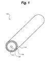
- Fig. 1 shows a structure of a conventional coaxial cable. Disposed at the center of a coaxial cable 120 is a signal line 121. Disposed around the signal line 121 is dielectric substance 122. Disposed outmost around the dielectric substance 122 is a ground layer 123. The outermost periphery of the coaxial cable is coated with an insulator 124. Thus, since the cross section of the coaxial cable 120 is circular, it cannot be flattened. Consequently, the coaxial cable 120 has a large diameter. Thus, the coaxial cable 120 cannot be densely mounted. In addition, since these layers should be cylindrically formed and deposited, a complicated producing process is required. Thus, it is difficult to suppress the production cost of the coaxial cable 120.
- patent document 1 and patent document 2 propose structures for mounting a plurality of signal lines in flat cables using liquid crystal polymer.
- Patent document 1 Japanese patent laid-open publication No. 2001-135974
- Patent document 2 Japanese patent laid-open publication No. HEI 11-162267.
- patent document 3 discloses a method for forming a radio frequency transmission line on a printed circuit board.
- Patent document 3 Japanese patent laid-open publication No. 2002-111233
- the flat cables disclosed in these patent documents 1 and 2 cannot be suitably used for transmitting radio frequency signals.
- the sizes of the cross sections of the signal lines, thicknesses of the dielectric substances, and so forth should be adjusted so that predetermined characteristic impedance can be obtained and insertion loss can be decreased.
- the ground layer should be sufficiently wider than the signal line so as to prevent signals from leaking out of the cable.
- Embodiments of the present invention seek to provide a flat cable that can be flexibly wired. Embodiments of the present invention also seek to adjust the size of the cross section of a signal line for designated characteristic impedance and to provide a flat cable having a sufficiently wider ground layer than the signal line.
- embodiments of the present invention seek to provide a flat cable that can be produced at low cost and can be densely mounted.
- a first aspect of the present invention provides a flat cable, comprising: a signal line; a dielectric sheet with which the signal line is coated; two ground layers that sandwich the dielectric sheet in its thickness direction, that extend in parallel in the longitudinal direction of the signal line, and that are spaced apart from each other; and a first insulator that coats the two ground layers so that they are not exposed to the outside.
- a second aspect of the present invention provides a flat cable, comprising: a dielectric sheet; a signal line formed on the dielectric sheet almost in parallel with its longitudinal direction; a first ground layer formed on the dielectric sheet almost in parallel with its longitudinal direction and spaced apart from the signal line; a second ground layer formed on the dielectric sheet almost in parallel with its longitudinal direction and spaced apart from the signal line, the signal line being formed between the first ground layer and the second ground layer; and upper and lower insulators formed on the upper side and the lower side of the dielectric sheet on which the signal line, the first ground layer, and the second ground layer are formed, respectively.
- a third aspect of the present invention provides a flat cable sheet, comprising: a plurality of signal lines spaced apart from each other; a dielectric sheet with which each of the signal lines is coated; two ground layers that sandwich the dielectric sheet in its thickness direction, that extend in parallel in the longitudinal direction of each of the signal lines, and that are spaced apart from each other; and an insulator that coats the two ground layers so that they are not exposed to the outside, wherein the signal lines are integrally coated with the dielectric sheet and the insulator.
- a fourth aspect of the present invention provides a flat cable sheet, comprising: a plurality of signal lines spaced apart from each other; a dielectric sheet with which each of the signal lines is coated; two ground layers that sandwich the dielectric sheet in its thickness direction, that extend in parallel in the longitudinal direction of each of the signal lines, and that are spaced apart from each other; a first insulator that coats the two ground layers so that they are not exposed to the outside; two shield layers that sandwich the first insulator in its thickness direction, that extend in parallel in the longitudinal direction of each of the signal lines, and that are spaced apart from each other; and a second insulator that coats the shield layers so that they are not exposed to the outside, wherein the signal lines are integrally coated with the dielectric sheet and the second insulator.
- a fifth aspect of the present invention provides a flat cable sheet producing method, comprising the steps of: (a) depositing a metal film on a first dielectric substance; (b) processing an upper portion of the first dielectric substance; (c) processing a lower portion of the first dielectric substance; (b1) etching the metal film so as to form a plurality of signal lines that are almost in parallel with each other; (b2) depositing a second dielectric substance on the front surface on the metal film etched at the first etching step (b1); (b3) depositing a metal film above the second dielectric substance deposited at the second depositing step (b2); (b4) forming the metal film deposited at the third depositing step (b3) as a plurality of ground layers spaced apart from each other and etching each of the ground layers so that they are formed above the signal lines; and (b5) depositing an insulator on the front surface of the metal film etched at the second etching step (b4), wherein the second processing step (c) comprises the steps of: (
- the size of the cross section of a signal line, the thickness of dielectric substance, and so forth are adjusted for predetermined characteristic impedance.
- a flat cable composed of a ground layer that is sufficiently wider than a signal line and a dielectric sheet that has plasticity can be produced at low cost.
- it can be miniaturized.
- an antenna portion is disposed at an upper portion of a liquid crystal display portion (inside a liquid crystal panel) so as to increase signal transmission/reception sensitivity against an access point.
- a radio communication module is disposed below a keyboard.
- the flat cable according to the present invention can be used to connect the antenna and the radio communication module.
- a radio frequency signal as high as 2.4 GHz is transmitted between the antenna and the radio communication module.
- the radio communication function can be mounted in a small space of a mobile apparatus.
- the flat cable according to embodiments of the present invention is a ribbon type cable, it needs a small space to mount. With the flat cable, a liquid crystal panel can be bent. Moreover, the flat cable can be mounted in a very limited space.
- a flat cable according to an embodiment of the present invention is a transmission line that transmits a radio frequency signal and that is produced by forming a signal line on the front surface of a bendable (flexible) dielectric substance (sheet) such as a liquid crystal polymer or Teflon (trademark of Dupont Inc.) substrate or therein and forming on the signal line a ground layer made of a metal through the dielectric substance.
- a bendable (flexible) dielectric substance such as a liquid crystal polymer or Teflon (trademark of Dupont Inc.) substrate or therein and forming on the signal line a ground layer made of a metal through the dielectric substance.
- two ground layers may be formed on the front surface of the dielectric sheet with a signal line between the two ground layers.
- the characteristic impedance of the signal line needs to be a predetermined value for example 50 ⁇ .
- the characteristic impedance of the signal line depends on its shape, the relative dielectric constant of the dielectric substance, and so forth.
- the ground layer needs to be sufficiently wider than the signal line.
- it is effective to coat a transmission line of which the signal line and the ground line are paired with a shield layer made of a metal.
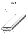
- Fig. 2 shows a structure of a flat cable according to a first embodiment of the present invention.
- a cable 10 is a radio frequency cable that has a strip line structure. Since this cable is flat, it can be more flattened than conventional coaxial cables. In addition, when the dielectric substance is thinned and the ground layer is more sufficiently widened than the signal line, the radiation of a signal from the side portion free of the ground layer can be suppressed.
- the characteristic impedance depends on the size of the cross section of the signal line, the specific dielectric constant of the dielectric substance, and so forth. In this example, the flat cable is designated to have a characteristic impedance of 50 Q.
- the cable 10 is structured so that a signal line 11 is coated with a thin dielectric sheet 12 and ground layers 13 are formed on an upper surface and a lower surface of the dielectric sheet 12, the ground layers 13 being sufficiently wider than the signal line 11.
- the upper and lower surface of the cable are coated with films of an insulator 14.
- the two ground layers are coated with two films of the insulator 14 so that the ground layers are not exposed to the outside.
- the side portions of the cable 10 are composed of the dielectric sheet 12 and the insulator 14.
- the dielectric sheet 12 is made of a material having plasticity. Thus, since the cable 10 can be relatively freely bent, it can be used for a complicated line and an open/close mechanism.
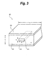
- FIG. 3 schematically shows a structure of a strip line.
- a strip line 20 is composed of a signal line 21, a dielectric sheet 22, and upper and lower ground layers 23.
- the width of each of the ground layers 23 is denoted by w
- the height of the dielectric sheet 22 is denoted by h
- the width of the cross section of the signal line 21 is denoted by a
- the height thereof is denoted by b
- the relative dielectric constant of the dielectric sheet 22 is denoted by ⁇ r .
- the characteristic impedance Z 0 can be approximately represented by the following formula 1.
- Z 0 (60 / ⁇ r ) 1 ⁇ 2 ) ln (4h / (0.67 ⁇ a (0.8 + (b / a))))
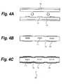
- Fig. 4A, Fig. 4B, Fig. 4C, and Fig. 5 are sectional views showing a method for producing the flat cable according to the first embodiment of the present invention.
- the signal line 11 is accurately formed by an etching process or the like.
- the upper and lower surfaces of the signal line 11 are coated with the dielectric sheets 12 and metal films.
- the material of the signal line 11 is for example copper.
- the metal films are processed by an etching process or the like so as to form the ground layers 13.
- the ground layers 13 are processed so that each of them is sufficiently wider than the signal line 11.
- the insulators 14 are formed on the upper and lower ground layers 13. As a result, a flat cable sheet 30 having a plurality of cables is produced.
- each of the ground layers 13 should be narrower than the cut interval so that the ground layers 13 are not cut.
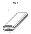
- a cable 40 shown in Fig. 6 contains a signal line 41, a dielectric sheet 42, upper and lower ground layers 43, upper and lower shield layers 44, and upper and lower insulators 45.
- the signal line 41 is coated with the dielectric sheet 42.
- the upper and lower ground layers 43 are formed on the upper and lower surfaces of the dielectric sheet 42, respectively. Each of the ground layers 43 is sufficiently wider than the signal line 41.
- the upper and lower ground layer 43 are coated with the upper and lower insulators 45, respectively.
- the upper and lower shield layers 44 are formed on the upper and lower insulators 45, respectively.
- the upper and lower shield layers 44 are coated with the upper and lower insulators 45, respectively.
- the shield layers 44 and the insulators 45 are formed on the upper and lower surfaces of the cable 10 of the first embodiment.
- the cable 40 With the cable 40, the radiation of a signal is more suppressed than with the cable 10 of the first embodiment. Thus, the influence of external electromagnetic noise against the signal line can be more suppressed than the first embodiment.
- the ground layers 43 and the shield layers 44 are not exposed to the outside.
- the side portions of the cable 40 are composed of the dielectric sheet 42 and the insulator 45.
- the cable 40 is produced in the same method shown in Fig. 4A to Fig. 4C and Fig. 5 except that after the flat cable sheet 30 shown in Fig. 4A to Fig. 4C is produced, the shield layers 44 are formed and etched and then the outermost insulators 45 are formed.
- the dielectric sheet 42 is made of a material having for example plasticity.
- a cable 50 shown in Fig. 7 is a cable having a coplanar structure of which a signal line 51 and two ground layers 53 are formed on the same plane (of a dielectric sheet 52). Since the signal line 51 and the two ground layers 53 are formed on the same plane, namely on the dielectric sheet 52, the structure of this cable becomes simpler and it can be produced at lower cost than the foregoing cables.
- the cable 50 is composed of a signal line 51, a dielectric sheet 52, two ground layers 53, and upper and lower insulators 54. As described above, the signal line 51 and the two ground layers 53 are formed almost in parallel in the longitudinal direction of the cable 50 so that the signal line 51 does not contact the two ground layer 53. In addition, the two ground layers 53 are formed on both sides of the signal line 51. In the cross section perpendicular to the longitudinal direction of the cable 50, each of the ground layers 53 is sufficiently wider than the signal line 51.
- the cable 50 can be produced in the same method as the foregoing embodiments shown in Fig. 4A to Fig. 4C, and Fig. 5.
- the signal line 51 and the two ground layers 53 are formed and etched in the same process as the foregoing embodiments.
- the dielectric sheet 52 is made of a material having for example plasticity.
- a coplanar waveguide 60 shown in Fig. 8 has the same structure as the cable 50 of the third embodiment.
- the coplanar waveguide 60 is composed of a signal line 61, a dielectric sheet 62, two ground layers 63, and an insulator 64.
- the relative dielectric constant of the dielectric sheet 62 is denoted by ⁇ r
- the thickness of the dielectric sheet 62 is denoted by h
- the width of the cross section of the signal line 61 is denoted by s
- the width of the signal line 61 when the waveguide is processed is denoted by w.
- the characteristic impedance Z 0 can be approximately expressed by a predetermined formula based on these values.
- the characteristic impedance Z 0 can be calculated using a predetermined simulator.
- a cable 70 shown in Fig. 9 is a part of an end portion (terminal portion) of a flat cable.
- the cable 70 is composed of a signal line 71, a dielectric sheet 72, upper and lower ground layers 73, and upper and lower insulators 74.
- the cable 70 has four through-holes 75 and one through-hole 76. Although the upper and lower ground layers 73 are exposed from the side portions of the cable 70, one of the flat cables of the first to third embodiments can be used.
- the four through-holes 75 electrically connect the upper and lower ground layers 73.
- the through-hole 76 is formed as a terminal with which a signal of the signal line 71 is connected to the outside. A terminal is disposed above the cable 70 shown in Fig. 9.
- the four through-holes 75 are formed.
- the number of through-holes 75 is not limited to four.
- the through-holes 75 are formed so that the potentials of the upper and lower ground layers 73 become equal.
- the through-holes can be formed in various methods.
- holes are made in two ground layers that sandwich a dielectric sheet.
- the holes are filled with electro-conductive paste (for example, silver paste or copper paste) so as to electrically connect the two ground layers.
- electro-conductive paste for example, silver paste or copper paste
- the walls of the holes are plated with electro-conductive substance so as to electrically connect the two ground layers.
- the first method is used.
- the cable 70 can be produced in the same method as the first embodiment shown in Fig. 4A to Fig. 4C and Fig. 5.
- the through-holes 75 and the through-holes 76 are formed by a single process.
- the dielectric sheet 72 is made of a material having for example plasticity.
- Fig. 10 is a sectional view seen in the direction of arrow A shown in Fig. 9.
- the through-holes 75 extend from the upper ground layer 73 to the lower ground layer 73.
- the through-holes 75 electrically connect the upper ground layer 73 and the lower ground layer 73.
- a space portion 80 that is concentrically cut from the upper ground layer 73 around the through-hole 76 keeps it apart from the upper ground layer 73.
- a space portion 81 that is concentrically cut from the lower ground layer 73 around the through-hole 76 keeps it apart from the lower ground layer 73.
- the space portion 81 may be formed in the same shape as the space portion 80.
- the through-hole 76 is connected to the signal line 71.
- the signal line 71 extends from the deeper side to the through-hole 76.
- the cable 70 that has such a structure, by connecting a ground of a circuit board to any external portion of the space portion 80 of the upper ground layer 73 and connecting a signal input/output portion of the circuit board to any portion of the space portion 80 of the ground layer 73, the circuit board and the cable 70 are electrically connected. These connections are performed by for example soldering. Alternatively, the circuit board and the cable 70 can be mechanically contacted or connected by for example clamping.
- Fig. 11A and Fig. 11B show a cable 85 according to an embodiment of the present invention along with a connector 90 electrically connected to the cable 85.
- Fig. 11A is a front view showing the cable 85 and the connector 90.
- Fig. 11B is a side view showing the cable 85 and the connector 90.
- a connector 90 is connected to an end portion of the cable 85 as shown in Fig. 11A and Fig. 11B.
- a ground terminal 91 of the connector 90 is connected to a ground layer 88 of the cable 85 by for example clamping. It is preferred that the ground terminal 91 should be connected to two ground layers 88 so that the potentials of the two ground layers 88 becomes equal. As with the fourth embodiment, through-holes that connect the two ground layers may be formed adjacent to the connector 90.
- a mate connector that fits the connector 90 is disposed on a circuit board. When these connectors are connected, the cable 85 and the circuit board can be easily connected.
- the cable 85 and the connector 90 may be electrically connected. In this case, the cable 85 and the connector 90 may be disconnectable.
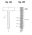
- Fig. 12A is a front view showing a cable 100.
- Fig. 12B is a sectional view showing the cable 100 taken along dotted line C of Fig. 12A.
- the cable 100 is formed in a T-letter shape.
- a forward end of the cable 100 functions as a dipole antenna.
- Connected to the dipole antenna is the flat cable according to an embodiment of the present invention.
- the flat cable is composed of a signal line 101, two dielectric sheets 102, two ground layers 103, and two insulators 104. These structural elements extend to the dipole antenna portion.
- Fig. 13A to Fig. 14 show arrangements of the signal line 101, the two dielectric sheets 102, the two ground layers 103, and the two insulators 104, which extend to the dipole antenna portion.
- Fig. 13A is a sectional view showing the flat cable along a layer denoted by arrow a of Fig. 12B (namely, the first ground layer 103).
- Fig. 13B is a sectional view showing the flat cable along a layer denoted by arrow b of Fig. 12B (namely, the signal line 101).
- Fig. 13C is a sectional view showing the flat cable along a layer denoted by arrow c shown in Fig. 12B (namely, the second ground layer 103).
- Fig. 13A shows that the first ground layer 103 extends from the flat cable to the left of the dipole antenna portion.
- Fig. 13B shows that the signal line that is narrower than each of the ground layers 103 extends from the flat cable to the right of the dipole antenna portion.
- Fig. 13C shows that the second ground layer 103 extends to the dipole antenna portion as with the first ground layer 103 shown in Fig. 13A.
- the cable 100 other than the antenna portion is produced in the same method as the first embodiment shown in Fig. 4A to Fig. 4C and Fig. 5.
- the two dielectric sheets 102 are made of a material having for example plasticity.
- Fig. 14A is a front view showing a cable 110.
- Fig. 14B is a sectional view showing the cable 110 taken along dotted line D of Fig. 14A.
- the cable 110 is formed in a strip shape.
- a forward end of the cable 110 functions as a sleeve antenna.
- Connected to the sleeve antenna is the flat cable according to an embodiment of the present invention.
- the flat cable is composed of a signal line 111, two dielectric sheets 112, two ground layers 113, and two insulators 114. These structural elements extend to the sleeve antenna portion.
- Fig. 15A to Fig. 15C show arrangements of the signal line 111, the two dielectric sheets 112, the two ground layers 113, and the two insulators 114, which extend to the sleeve antenna portion.
- Fig. 15A is a sectional view showing the flat cable along a layer denoted by arrow d of Fig. 14B (namely, the first ground layer 113).
- Fig. 15B is a sectional view showing the flat cable along a layer denoted by arrow e of Fig. 14B (namely, the signal line 111).
- Fig. 15C is a sectional view showing the flat cable along a layer denoted by arrow f of Fig. 14B (namely, the second ground layer 113).
- Fig. 15A shows that the first ground layer 113 extends from the flat cable to almost the middle position of the sleeve antenna portion.
- Fig. 15B shows that the signal line 111 that is narrower than each of the ground layers 113 extends from the flat cable to the endmost portion of the sleeve antenna portion. However, from the middle position of the sleeve antenna portion to the endmost portion thereto, the signal line 111 has almost the same width as each of the ground layers 113.
- Fig. 15C shows that the second ground layer 113 extends from the flat cable to the sleeve antenna portion as with the first ground layer 113 shown in Fig. 15A.
- the cable 100 other than the antenna portion is produced in the same method as the first embodiment shown in Fig. 4A to 4C and Fig. 5.
- the dielectric sheet 102 is made of a material having for example plasticity.
- the cables according to the sixth and seventh embodiments are integrated with an antenna
- the flat cables according to an embodiment of the present invention can be integrated with various types of antennas.
- the present invention is not limited to the foregoing embodiments. These cables and antennas can be simultaneously produced in the same process.
Landscapes
- Engineering & Computer Science (AREA)
- Architecture (AREA)
- Civil Engineering (AREA)
- Structural Engineering (AREA)
- Insulated Conductors (AREA)
- Waveguides (AREA)
Abstract
Description
Claims (28)
- A flat cable, comprising:a signal line;a dielectric sheet with which the signal line is coated;two ground layers that sandwich the dielectric sheet in its thickness direction, that extend in parallel in the longitudinal direction of the signal line, and that are spaced apart from each other; anda first insulator that coats the two ground layers so that they are not exposed to the outside.
- The flat cable as set forth in claim 1,
wherein the size of the cross section of the signal line, the thickness of the dielectric sheet, and the relative dielectric constant of the dielectric sheet are adjusted for predetermined characteristic impedance. - The flat cable as set forth in claim 1, further comprising:two shield layers that sandwich the first insulator in its thickness direction, that extend in parallel in the longitudinal direction of the signal line, and that are spaced apart from each other; anda second insulator that coats the shield layers so that they are not exposed to the outside.
- The flat cable as set forth in claim 1,
wherein the dielectric sheet has plasticity. - The flat cable as set forth in claim 1,
wherein the width of each of the two ground layers in a first direction perpendicular to the longitudinal direction of the signal line is sufficiently larger than the width of the signal line in the first direction. - The flat cable as set forth in claim 1,
wherein the two ground layers are connected with at least one though-hole formed in at least one end portion of the flat cable. - The flat cable as set forth in claim 1,
wherein an antenna portion is integrally connected to one end portion of the flat cable, and
wherein the signal line and the two ground layers extend to the antenna portion. - A flat cable, comprising:a dielectric sheet;a signal line formed on the dielectric sheet almost in parallel with its longitudinal direction;a first ground layer formed on the dielectric sheet almost in parallel with its longitudinal direction and spaced apart from the signal line;a second ground layer formed on the dielectric sheet almost in parallel with its longitudinal direction and spaced apart from the signal line, the signal line being formed between the first ground layer and the second ground layer; andupper and lower insulators formed on the upper side and the lower side of the dielectric sheet on which the signal line, the first ground layer, and the second ground layer are formed, respectively.
- The flat cable as set forth in claim 8,
wherein the size of the cross section of the signal line, the thickness of the dielectric sheet, and the relative dielectric constant of the dielectric sheet are adjusted for predetermined characteristic impedance. - The flat cable as set forth in claim 8,
wherein the dielectric sheet has plasticity. - The flat cable as set forth in claim 8,
wherein the width of each of the two ground layers in a first direction perpendicular to the longitudinal direction of the signal line is sufficiently larger than the width of the signal line in the first direction. - The flat cable as set forth in claim 8,
wherein the first and second ground layers are connected with at least one though-hole formed in at least one end portion of the flat cable. - The flat cable as set forth in claim 8,
wherein an antenna portion is integrally connected to one end portion of the flat cable, and
wherein the signal line and the two ground layers extend to the antenna portion. - A flat cable sheet, comprising:wherein the signal lines are integrally coated with the dielectric sheet and the insulator.a plurality of signal lines spaced apart from each other;a dielectric sheet with which each of the signal lines is coated;two ground layers that sandwich the dielectric sheet in its thickness direction, that extend in parallel in the longitudinal direction of each of the signal lines, and that are spaced apart from each other; andan insulator that coats the two ground layers so that they are not exposed to the outside,
- The flat cable sheet as set forth in claim 14,
wherein a plurality of flat cables are obtained by cutting the flat cable sheet, and
wherein the size of the cross section of each of the signal lines, the thickness of the dielectric sheet, and the relative dielectric constant of the dielectric sheet are adjusted for predetermined characteristic impedance. - The flat cable sheet as set forth in claim 14,
wherein regions free of the two ground layers are formed between any adjacent two of the signal lines in their longitudinal direction; and
wherein the flat cable sheet is cut into pieces along the regions. - The flat cable sheet as set forth in claim 14,
wherein the dielectric sheet has plasticity. - The flat cable sheet as set forth in claim 14,
wherein the width of each of the two ground layers in a first direction perpendicular to the longitudinal direction of each of the signal lines is sufficiently larger than the width of each of the signal lines in the first direction. - The flat cable sheet as set forth in claim 14,
wherein the two ground layers are connected with at least one though-hole that is formed corresponding to each of the signal lines in at least one end portion of the flat cable sheet. - A flat cable sheet, comprising:wherein the signal lines are integrally coated with the dielectric sheet and the second insulator.a plurality of signal lines spaced apart from each other;a dielectric sheet with which each of the signal lines is coated;two ground layers that sandwich the dielectric sheet in its thickness direction, that extend in parallel in the longitudinal direction of each of the signal lines, and that are spaced apart from each other;a first insulator that coats the two ground layers so that they are not exposed to the outside;two shield layers that sandwich the first insulator in its thickness direction, that extend in parallel in the longitudinal direction of each of the signal lines, and that are spaced apart from each other; anda second insulator that coats the shield layers so that they are not exposed to the outside,
- The flat cable sheet as set forth in claim 20,
wherein a plurality of flat cables are obtained by cutting the flat cable sheet, and
wherein the size of the cross section of each of the signal lines, the thickness of the dielectric sheet, and the relative dielectric constant of the dielectric sheet are adjusted for predetermined characteristic impedance. - The flat cable sheet as set forth in claim 20,
wherein regions free of the two ground layers and the two shield layers are formed between any adjacent two of the signal lines in their longitudinal direction; and
wherein the flat cable sheet is cut into pieces along the regions. - The flat cable sheet as set forth in claim 20,
wherein the dielectric sheet has plasticity. - The flat cable sheet as set forth in claim 20,
wherein the width of each of the two ground layers in a first direction perpendicular to the longitudinal direction of each of the signal lines is sufficiently larger than the width of each of the signal lines in the first direction. - The flat cable sheet as set forth in claim 20,
wherein the two ground layers are connected with at least one though-hole that is formed corresponding to each of the signal lines in at least one end portion of the flat cable sheet. - A flat cable sheet producing method, comprising the steps of:(a) depositing a metal film on a first dielectric substance;(b) processing an upper portion of the first dielectric substance;(c) processing a lower portion of the first dielectric substance;(b1) etching the metal film so as to form a plurality of signal lines that are almost in parallel with each other;(b2) depositing a second dielectric substance on the front surface on the metal film etched at the first etching step (b1);(b3) depositing a metal film above the second dielectric substance deposited at the second depositing step (b2);(b4) forming the metal film deposited at the third depositing step (b3) as a plurality of ground layers spaced apart from each other and etching each of the ground layers so that they are formed above the signal lines; and(b5) depositing an insulator on the front surface of the metal film etched at the second etching step (b4),
wherein the second processing step (c) comprises the steps of:(c1) depositing a metal film below the first dielectric substance;(c2) forming the metal film deposited at the fifth depositing step (c1) as a plurality of ground layers spaced apart from each other and etching the ground layers so that they are formed below the signal lines; and(c3) depositing an insulator on the front surface of the metal film etched at the third etching step (c2), and
wherein the first processing step and the second processing step are performed in any order. - The flat cable sheet producing method as set forth in claim 26,
wherein the first processing step (b) comprises the steps of:(b6) depositing a metal film above the insulator deposited at the fourth depositing step (b5);(b7) forming the metal film deposited at the seventh depositing step (b6) as a plurality of shield layers spaced apart from each other and etching the shield layers so that they are formed above the ground layers; and(b8) depositing an insulator on the front surface of the shield layers etched at the fourth etching step (b7), and
wherein the second processing step (c) comprises the steps of:(b9) depositing a metal film below the insulator deposited at the sixth depositing step (c3);(b10) forming the metal film deposited at the ninth depositing step (b9) as a plurality of shield layers spaced apart from each other and etching the shield layers so that they are formed below the ground layers; and(b11) depositing an insulator on the front surface of the shield layers etched at the fifth etching step(b10) . - The flat cable sheet producing method as set forth in claim 26,
wherein the width of each of the ground layers in a first direction perpendicular to the longitudinal direction of each of the signal lines is sufficiently larger than the width of each of the signal lines in the first direction.
Applications Claiming Priority (2)
| Application Number | Priority Date | Filing Date | Title |
|---|---|---|---|
| JP2004065146A JP3982511B2 (en) | 2004-03-09 | 2004-03-09 | Flat cable manufacturing method |
| JP2004065146 | 2004-03-09 |
Publications (2)
| Publication Number | Publication Date |
|---|---|
| EP1575062A2 true EP1575062A2 (en) | 2005-09-14 |
| EP1575062A3 EP1575062A3 (en) | 2006-03-29 |
Family
ID=34824546
Family Applications (1)
| Application Number | Title | Priority Date | Filing Date |
|---|---|---|---|
| EP05251394A Withdrawn EP1575062A3 (en) | 2004-03-09 | 2005-03-08 | Flat cable, flat cable sheet, and flat cable sheet producing method |
Country Status (5)
| Country | Link |
|---|---|
| US (1) | US7196273B2 (en) |
| EP (1) | EP1575062A3 (en) |
| JP (1) | JP3982511B2 (en) |
| KR (1) | KR20060043490A (en) |
| CN (1) | CN100367417C (en) |
Cited By (3)
| Publication number | Priority date | Publication date | Assignee | Title |
|---|---|---|---|---|
| EP2017920A1 (en) * | 2007-07-19 | 2009-01-21 | Brocoli, Ltd. | Flat uniform transmission line having electromagnetic shielding function |
| WO2011095206A1 (en) * | 2010-02-03 | 2011-08-11 | Laird Technologies Ab | Signal transmission device and portable radio communication device comprising such a signal transmission device |
| EP4440259A4 (en) * | 2022-10-31 | 2025-04-30 | Honor Device Co., Ltd. | Electronic assembly and terminal device |
Families Citing this family (35)
| Publication number | Priority date | Publication date | Assignee | Title |
|---|---|---|---|---|
| JP2007193999A (en) * | 2006-01-17 | 2007-08-02 | Sony Chemical & Information Device Corp | Transmission cable |
| KR20080054951A (en) * | 2006-12-14 | 2008-06-19 | 삼성전자주식회사 | Handheld terminal |
| EP2232631B1 (en) * | 2007-11-15 | 2015-03-18 | Loc8tor Ltd | Locating system |
| US8067701B2 (en) * | 2008-01-07 | 2011-11-29 | Apple Inc. | I/O connectors with extendable faraday cage |
| US8110744B2 (en) | 2008-08-19 | 2012-02-07 | Apple Inc. | Flexible shielded cable |
| US7804029B1 (en) * | 2008-12-05 | 2010-09-28 | The United States Of America As Represented By The United States Department Of Energy | Electromagnetic wrap |
| CN101840749B (en) * | 2009-03-20 | 2012-05-23 | 住友电气工业株式会社 | Shielded flat cable |
| US8212634B2 (en) * | 2009-06-04 | 2012-07-03 | International Business Machines Corporation | Vertical coplanar waveguide with tunable characteristic impedance design structure and method of fabricating the same |
| WO2010148165A2 (en) | 2009-06-19 | 2010-12-23 | 3M Innovative Properties Company | Shielded electrical cable |
| US9685259B2 (en) | 2009-06-19 | 2017-06-20 | 3M Innovative Properties Company | Shielded electrical cable |
| CN102484312B (en) * | 2009-08-20 | 2014-06-25 | 株式会社村田制作所 | Antenna module |
| US9577305B2 (en) * | 2011-08-12 | 2017-02-21 | Commscope Technologies Llc | Low attenuation stripline RF transmission cable |
| US8723042B2 (en) * | 2011-03-17 | 2014-05-13 | Electronics And Telecommunications Research Institute | Flexible flat cable and manufacturing method thereof |
| US20130111743A1 (en) * | 2011-11-07 | 2013-05-09 | Chien-Han Ho | Method for manufacturing flat coaxial cable |
| WO2013069763A1 (en) * | 2011-11-10 | 2013-05-16 | 株式会社村田製作所 | High frequency signal line and electronic device provided with same |
| KR20160010469A (en) * | 2013-04-24 | 2016-01-27 | 가부시키가이샤 쇼난 고세이쥬시 세이사쿠쇼 | Signal transmission flat cable |
| US9241400B2 (en) * | 2013-08-23 | 2016-01-19 | Seagate Technology Llc | Windowed reference planes for embedded conductors |
| JP6368078B2 (en) * | 2013-09-25 | 2018-08-01 | 日本シイエムケイ株式会社 | Printed wiring board |
| US20160329130A1 (en) * | 2015-05-07 | 2016-11-10 | Wilson Electronics, Llc | Flat coaxial cable |
| MX387759B (en) | 2017-11-16 | 2025-03-14 | Norman R Byrne | DATA OR ELECTRICAL POWER DISTRIBUTION SYSTEM. |
| US10910692B2 (en) * | 2017-11-28 | 2021-02-02 | Taoglas Group Holdings Limited | In-glass high performance antenna |
| JP6642783B2 (en) | 2017-12-28 | 2020-02-12 | 株式会社村田製作所 | Transmission line equipment |
| JP7067275B2 (en) * | 2018-05-30 | 2022-05-16 | 住友電気工業株式会社 | Shielded flat cable |
| JP2020024901A (en) * | 2018-08-02 | 2020-02-13 | Kmt技研株式会社 | Shielded thin flat cable, and manufacturing method thereof |
| US11108141B2 (en) | 2018-09-12 | 2021-08-31 | Taoglas Group Holdings Limited | Embedded patch antennas, systems and methods |
| TWI696197B (en) * | 2018-11-21 | 2020-06-11 | 貿聯國際股份有限公司 | High frequency flexible flat cable |
| US11303079B2 (en) | 2019-05-28 | 2022-04-12 | Norman R. Byrne | Modular electrical system |
| KR102733474B1 (en) * | 2019-07-25 | 2024-11-25 | 삼성전자 주식회사 | Flexible flat cable and method for manufacturing the same |
| CN110729074A (en) * | 2019-11-14 | 2020-01-24 | 中航富士达科技股份有限公司 | Flexible ribbon cable and radio frequency assembly |
| CN111524643A (en) * | 2020-05-19 | 2020-08-11 | 苏州硕贝德创新技术研究有限公司 | Easily-bent flexible transmission line |
| US11875912B2 (en) * | 2020-07-02 | 2024-01-16 | Sumitomo Electric Industries, Ltd. | Shielded flat cable |
| WO2023075141A1 (en) * | 2021-10-27 | 2023-05-04 | 삼성전자 주식회사 | Electronic device comprising rf cable |
| EP4425710A4 (en) | 2021-10-27 | 2025-02-26 | Samsung Electronics Co., Ltd. | ELECTRONIC DEVICE COMPRISING RF CABLE |
| TWI826947B (en) * | 2022-03-07 | 2023-12-21 | 貝爾威勒電子股份有限公司 | Flexible flat cable |
| US20250273885A1 (en) * | 2024-02-28 | 2025-08-28 | International Business Machines Corporation | Flat flexible cable with embedded ground plane |
Family Cites Families (28)
| Publication number | Priority date | Publication date | Assignee | Title |
|---|---|---|---|---|
| US3612744A (en) * | 1969-02-27 | 1971-10-12 | Hughes Aircraft Co | Flexible flat conductor cable of variable electrical characteristics |
| US3763306A (en) * | 1972-03-17 | 1973-10-02 | Thomas & Betts Corp | Flat multi-signal transmission line cable with plural insulation |
| US4616102A (en) * | 1980-02-21 | 1986-10-07 | Thomas & Betts Corporation | Flat conductor electrical cable assembly |
| US4481379A (en) * | 1981-12-21 | 1984-11-06 | Brand-Rex Company | Shielded flat communication cable |
| US4551576A (en) * | 1984-04-04 | 1985-11-05 | Parlex Corporation | Flat embedded-shield multiconductor signal transmission cable, method of manufacture and method of stripping |
| GB8424285D0 (en) * | 1984-09-26 | 1984-10-31 | Allied Corp | Electric cables |
| US4642480A (en) * | 1985-03-27 | 1987-02-10 | Amp Incorporated | Low profile cable with high performance characteristics |
| US4707671A (en) * | 1985-05-31 | 1987-11-17 | Junkosha Co., Ltd. | Electrical transmission line |
| US4698457A (en) * | 1985-09-25 | 1987-10-06 | Thomas & Betts Corporation | Strippable shielded electrical cable assembly |
| US4845311A (en) * | 1988-07-21 | 1989-07-04 | Hughes Aircraft Company | Flexible coaxial cable apparatus and method |
| US4926007A (en) | 1989-03-03 | 1990-05-15 | W. H. Brady Co. | Shielded flexible connector and process therefor |
| US4972041A (en) * | 1989-07-18 | 1990-11-20 | W. L. Gore & Associates, Inc. | Ribbon cables having wrapped drain wires |
| US5235132A (en) * | 1992-01-29 | 1993-08-10 | W. L. Gore & Associates, Inc. | Externally and internally shielded double-layered flat cable assembly |
| JP2594734Y2 (en) * | 1992-10-19 | 1999-05-10 | 住友電装株式会社 | Flat cable with shield |
| US5554825A (en) * | 1994-11-14 | 1996-09-10 | The Whitaker Corporation | Flexible cable with a shield and a ground conductor |
| US5552565A (en) * | 1995-03-31 | 1996-09-03 | Hewlett-Packard Company | Multiconductor shielded transducer cable |
| JPH11506865A (en) * | 1995-06-05 | 1999-06-15 | セクストン、ロバート・ジェイ | Flat surface-mounted multipurpose electric wire |
| FR2742258B1 (en) * | 1995-12-08 | 1998-02-27 | Axoncable Sa | LOW MARGIN FLAT CABLE |
| WO1998006243A1 (en) * | 1996-07-31 | 1998-02-12 | Dyconex Patente | Process for producing connecting conductors |
| US6633001B2 (en) * | 1996-10-31 | 2003-10-14 | Mag Holdings, Inc. | Lightning retardant cable and conduit systems |
| JP3522513B2 (en) | 1997-11-26 | 2004-04-26 | 山一電機株式会社 | Flat cable and method of manufacturing the same |
| CN1218005C (en) * | 1998-05-19 | 2005-09-07 | 索尼化学株式会社 | Adhesive and circuit material using adhesive |
| JP2001119460A (en) * | 1999-10-20 | 2001-04-27 | Fujitsu Ltd | Foldable mobile phone and flexible cable |
| JP3497110B2 (en) * | 1999-11-09 | 2004-02-16 | 山一電機株式会社 | Flat type shielded cable |
| JP2002111233A (en) * | 2000-10-03 | 2002-04-12 | Victor Co Of Japan Ltd | Printed wiring board and method of manufacturing the same |
| DE10060070C2 (en) * | 2000-12-01 | 2003-04-30 | Webasto Vehicle Sys Int Gmbh | Wiring harness arrangement, especially for vehicles |
| CN2545680Y (en) * | 2002-03-11 | 2003-04-16 | 凌君彦 | Flat foil audio transmission electric cable |
| EP1453068A1 (en) | 2003-02-26 | 2004-09-01 | I & T Flachleiter Produktions-Ges.m.b.h. | Flat conductor cable |
-
2004
- 2004-03-09 JP JP2004065146A patent/JP3982511B2/en not_active Expired - Fee Related
-
2005
- 2005-03-08 US US11/075,074 patent/US7196273B2/en not_active Expired - Fee Related
- 2005-03-08 KR KR1020050018963A patent/KR20060043490A/en not_active Abandoned
- 2005-03-08 EP EP05251394A patent/EP1575062A3/en not_active Withdrawn
- 2005-03-09 CN CNB2005100536700A patent/CN100367417C/en not_active Expired - Fee Related
Cited By (4)
| Publication number | Priority date | Publication date | Assignee | Title |
|---|---|---|---|---|
| EP2017920A1 (en) * | 2007-07-19 | 2009-01-21 | Brocoli, Ltd. | Flat uniform transmission line having electromagnetic shielding function |
| US7898355B2 (en) | 2007-07-19 | 2011-03-01 | Brocoli Ltd. | Flat uniform transmission line having electromagnetic shielding function |
| WO2011095206A1 (en) * | 2010-02-03 | 2011-08-11 | Laird Technologies Ab | Signal transmission device and portable radio communication device comprising such a signal transmission device |
| EP4440259A4 (en) * | 2022-10-31 | 2025-04-30 | Honor Device Co., Ltd. | Electronic assembly and terminal device |
Also Published As
| Publication number | Publication date |
|---|---|
| EP1575062A3 (en) | 2006-03-29 |
| JP3982511B2 (en) | 2007-09-26 |
| CN100367417C (en) | 2008-02-06 |
| US7196273B2 (en) | 2007-03-27 |
| US20050200557A1 (en) | 2005-09-15 |
| KR20060043490A (en) | 2006-05-15 |
| CN1667760A (en) | 2005-09-14 |
| JP2005259359A (en) | 2005-09-22 |
Similar Documents
| Publication | Publication Date | Title |
|---|---|---|
| EP1575062A2 (en) | Flat cable, flat cable sheet, and flat cable sheet producing method | |
| US10651526B2 (en) | Flexible flat cable comprising stacked insulating layers covered by a conductive outer skin and method for manufacturing | |
| US8440910B2 (en) | Differential signal transmission cable | |
| US7645941B2 (en) | Shielded flexible circuits and methods for manufacturing same | |
| US8440911B2 (en) | Flat cable | |
| US10178762B2 (en) | Device and method for transmitting differential data signals | |
| JP2006024618A (en) | Wiring board | |
| US8542159B2 (en) | Cable connector and antenna component | |
| CN104798248B (en) | Transmission line and electronic equipment | |
| US6809608B2 (en) | Transmission line structure with an air dielectric | |
| CN220021573U (en) | Transmission lines and electronic equipment | |
| CN118888188A (en) | Flexible Cable | |
| GB2518034B (en) | Flat cable and electronic device | |
| US20060061433A1 (en) | Printed board | |
| US20230260674A1 (en) | Hybrid cabling solution for higher bandwidth and millimeter wave applications | |
| JP4998741B2 (en) | Adapter structure, high-frequency cable body and wiring board connector | |
| JP6138422B2 (en) | Signal transmission line and manufacturing method thereof | |
| KR20080054670A (en) | High-frequency transmission line device capable of common mode filtering | |
| JP4084595B2 (en) | Manufacturing method of high frequency flexible multi-core coaxial cable and its applied electronic equipment | |
| CN211629302U (en) | Dual-polarized antenna and array | |
| CN111786096B (en) | Antenna and electronic equipment | |
| JP6333217B2 (en) | Method for producing hollow film cable | |
| JP2005174893A (en) | High-frequency use fpc & ffc connector | |
| CN117154408A (en) | Millimeter wave antenna components and display devices | |
| CN116567912A (en) | Embedded PCB transmission structure |
Legal Events
| Date | Code | Title | Description |
|---|---|---|---|
| PUAI | Public reference made under article 153(3) epc to a published international application that has entered the european phase |
Free format text: ORIGINAL CODE: 0009012 |
|
| AK | Designated contracting states |
Kind code of ref document: A2 Designated state(s): AT BE BG CH CY CZ DE DK EE ES FI FR GB GR HU IE IS IT LI LT LU MC NL PL PT RO SE SI SK TR |
|
| AX | Request for extension of the european patent |
Extension state: AL BA HR LV MK YU |
|
| PUAL | Search report despatched |
Free format text: ORIGINAL CODE: 0009013 |
|
| AK | Designated contracting states |
Kind code of ref document: A3 Designated state(s): AT BE BG CH CY CZ DE DK EE ES FI FR GB GR HU IE IS IT LI LT LU MC NL PL PT RO SE SI SK TR |
|
| AX | Request for extension of the european patent |
Extension state: AL BA HR LV MK YU |
|
| 17P | Request for examination filed |
Effective date: 20060623 |
|
| AKX | Designation fees paid |
Designated state(s): DE FR GB |
|
| STAA | Information on the status of an ep patent application or granted ep patent |
Free format text: STATUS: THE APPLICATION IS DEEMED TO BE WITHDRAWN |
|
| 18D | Application deemed to be withdrawn |
Effective date: 20121002 |