EP1571853A2 - Reflektive Flüssigkristallanzeige und Projektionsapparat - Google Patents
Reflektive Flüssigkristallanzeige und Projektionsapparat Download PDFInfo
- Publication number
- EP1571853A2 EP1571853A2 EP05004578A EP05004578A EP1571853A2 EP 1571853 A2 EP1571853 A2 EP 1571853A2 EP 05004578 A EP05004578 A EP 05004578A EP 05004578 A EP05004578 A EP 05004578A EP 1571853 A2 EP1571853 A2 EP 1571853A2
- Authority
- EP
- European Patent Office
- Prior art keywords
- liquid crystal
- crystal display
- reflection type
- type liquid
- display device
- Prior art date
- Legal status (The legal status is an assumption and is not a legal conclusion. Google has not performed a legal analysis and makes no representation as to the accuracy of the status listed.)
- Ceased
Links
Images


Classifications
-
- H—ELECTRICITY
- H04—ELECTRIC COMMUNICATION TECHNIQUE
- H04N—PICTORIAL COMMUNICATION, e.g. TELEVISION
- H04N9/00—Details of colour television systems
- H04N9/12—Picture reproducers
- H04N9/31—Projection devices for colour picture display, e.g. using electronic spatial light modulators [ESLM]
- H04N9/3102—Projection devices for colour picture display, e.g. using electronic spatial light modulators [ESLM] using two-dimensional electronic spatial light modulators
- H04N9/3105—Projection devices for colour picture display, e.g. using electronic spatial light modulators [ESLM] using two-dimensional electronic spatial light modulators for displaying all colours simultaneously, e.g. by using two or more electronic spatial light modulators
-
- A—HUMAN NECESSITIES
- A45—HAND OR TRAVELLING ARTICLES
- A45D—HAIRDRESSING OR SHAVING EQUIPMENT; EQUIPMENT FOR COSMETICS OR COSMETIC TREATMENTS, e.g. FOR MANICURING OR PEDICURING
- A45D34/00—Containers or accessories specially adapted for handling liquid toiletry or cosmetic substances, e.g. perfumes
- A45D34/04—Appliances specially adapted for applying liquid, e.g. using roller or ball
-
- A—HUMAN NECESSITIES
- A45—HAND OR TRAVELLING ARTICLES
- A45D—HAIRDRESSING OR SHAVING EQUIPMENT; EQUIPMENT FOR COSMETICS OR COSMETIC TREATMENTS, e.g. FOR MANICURING OR PEDICURING
- A45D40/00—Casings or accessories specially adapted for storing or handling solid or pasty toiletry or cosmetic substances, e.g. shaving soaps or lipsticks
- A45D40/26—Appliances specially adapted for applying pasty paint, e.g. using roller, using a ball
-
- G—PHYSICS
- G02—OPTICS
- G02F—OPTICAL DEVICES OR ARRANGEMENTS FOR THE CONTROL OF LIGHT BY MODIFICATION OF THE OPTICAL PROPERTIES OF THE MEDIA OF THE ELEMENTS INVOLVED THEREIN; NON-LINEAR OPTICS; FREQUENCY-CHANGING OF LIGHT; OPTICAL LOGIC ELEMENTS; OPTICAL ANALOGUE/DIGITAL CONVERTERS
- G02F1/00—Devices or arrangements for the control of the intensity, colour, phase, polarisation or direction of light arriving from an independent light source, e.g. switching, gating or modulating; Non-linear optics
- G02F1/01—Devices or arrangements for the control of the intensity, colour, phase, polarisation or direction of light arriving from an independent light source, e.g. switching, gating or modulating; Non-linear optics for the control of the intensity, phase, polarisation or colour
- G02F1/13—Devices or arrangements for the control of the intensity, colour, phase, polarisation or direction of light arriving from an independent light source, e.g. switching, gating or modulating; Non-linear optics for the control of the intensity, phase, polarisation or colour based on liquid crystals, e.g. single liquid crystal display cells
- G02F1/137—Devices or arrangements for the control of the intensity, colour, phase, polarisation or direction of light arriving from an independent light source, e.g. switching, gating or modulating; Non-linear optics for the control of the intensity, phase, polarisation or colour based on liquid crystals, e.g. single liquid crystal display cells characterised by the electro-optical or magneto-optical effect, e.g. field-induced phase transition, orientation effect, guest-host interaction or dynamic scattering
- G02F1/139—Devices or arrangements for the control of the intensity, colour, phase, polarisation or direction of light arriving from an independent light source, e.g. switching, gating or modulating; Non-linear optics for the control of the intensity, phase, polarisation or colour based on liquid crystals, e.g. single liquid crystal display cells characterised by the electro-optical or magneto-optical effect, e.g. field-induced phase transition, orientation effect, guest-host interaction or dynamic scattering based on orientation effects in which the liquid crystal remains transparent
- G02F1/1393—Devices or arrangements for the control of the intensity, colour, phase, polarisation or direction of light arriving from an independent light source, e.g. switching, gating or modulating; Non-linear optics for the control of the intensity, phase, polarisation or colour based on liquid crystals, e.g. single liquid crystal display cells characterised by the electro-optical or magneto-optical effect, e.g. field-induced phase transition, orientation effect, guest-host interaction or dynamic scattering based on orientation effects in which the liquid crystal remains transparent the birefringence of the liquid crystal being electrically controlled, e.g. ECB-, DAP-, HAN-, PI-LC cells
-
- A—HUMAN NECESSITIES
- A45—HAND OR TRAVELLING ARTICLES
- A45D—HAIRDRESSING OR SHAVING EQUIPMENT; EQUIPMENT FOR COSMETICS OR COSMETIC TREATMENTS, e.g. FOR MANICURING OR PEDICURING
- A45D34/00—Containers or accessories specially adapted for handling liquid toiletry or cosmetic substances, e.g. perfumes
- A45D2034/002—Accessories
-
- A—HUMAN NECESSITIES
- A45—HAND OR TRAVELLING ARTICLES
- A45D—HAIRDRESSING OR SHAVING EQUIPMENT; EQUIPMENT FOR COSMETICS OR COSMETIC TREATMENTS, e.g. FOR MANICURING OR PEDICURING
- A45D40/00—Casings or accessories specially adapted for storing or handling solid or pasty toiletry or cosmetic substances, e.g. shaving soaps or lipsticks
- A45D2040/0006—Accessories
-
- A—HUMAN NECESSITIES
- A45—HAND OR TRAVELLING ARTICLES
- A45D—HAIRDRESSING OR SHAVING EQUIPMENT; EQUIPMENT FOR COSMETICS OR COSMETIC TREATMENTS, e.g. FOR MANICURING OR PEDICURING
- A45D2200/00—Details not otherwise provided for in A45D
- A45D2200/05—Details of containers
- A45D2200/054—Means for supplying liquid to the outlet of the container
- A45D2200/056—Reciprocating pumps, i.e. with variable volume chamber wherein pressure and vacuum are alternately generated
-
- G—PHYSICS
- G02—OPTICS
- G02F—OPTICAL DEVICES OR ARRANGEMENTS FOR THE CONTROL OF LIGHT BY MODIFICATION OF THE OPTICAL PROPERTIES OF THE MEDIA OF THE ELEMENTS INVOLVED THEREIN; NON-LINEAR OPTICS; FREQUENCY-CHANGING OF LIGHT; OPTICAL LOGIC ELEMENTS; OPTICAL ANALOGUE/DIGITAL CONVERTERS
- G02F1/00—Devices or arrangements for the control of the intensity, colour, phase, polarisation or direction of light arriving from an independent light source, e.g. switching, gating or modulating; Non-linear optics
- G02F1/01—Devices or arrangements for the control of the intensity, colour, phase, polarisation or direction of light arriving from an independent light source, e.g. switching, gating or modulating; Non-linear optics for the control of the intensity, phase, polarisation or colour
- G02F1/13—Devices or arrangements for the control of the intensity, colour, phase, polarisation or direction of light arriving from an independent light source, e.g. switching, gating or modulating; Non-linear optics for the control of the intensity, phase, polarisation or colour based on liquid crystals, e.g. single liquid crystal display cells
- G02F1/133—Constructional arrangements; Operation of liquid crystal cells; Circuit arrangements
- G02F1/1333—Constructional arrangements; Manufacturing methods
- G02F1/1337—Surface-induced orientation of the liquid crystal molecules, e.g. by alignment layers
- G02F1/133742—Surface-induced orientation of the liquid crystal molecules, e.g. by alignment layers for homeotropic alignment
-
- G—PHYSICS
- G02—OPTICS
- G02F—OPTICAL DEVICES OR ARRANGEMENTS FOR THE CONTROL OF LIGHT BY MODIFICATION OF THE OPTICAL PROPERTIES OF THE MEDIA OF THE ELEMENTS INVOLVED THEREIN; NON-LINEAR OPTICS; FREQUENCY-CHANGING OF LIGHT; OPTICAL LOGIC ELEMENTS; OPTICAL ANALOGUE/DIGITAL CONVERTERS
- G02F1/00—Devices or arrangements for the control of the intensity, colour, phase, polarisation or direction of light arriving from an independent light source, e.g. switching, gating or modulating; Non-linear optics
- G02F1/01—Devices or arrangements for the control of the intensity, colour, phase, polarisation or direction of light arriving from an independent light source, e.g. switching, gating or modulating; Non-linear optics for the control of the intensity, phase, polarisation or colour
- G02F1/13—Devices or arrangements for the control of the intensity, colour, phase, polarisation or direction of light arriving from an independent light source, e.g. switching, gating or modulating; Non-linear optics for the control of the intensity, phase, polarisation or colour based on liquid crystals, e.g. single liquid crystal display cells
- G02F1/133—Constructional arrangements; Operation of liquid crystal cells; Circuit arrangements
- G02F1/136—Liquid crystal cells structurally associated with a semi-conducting layer or substrate, e.g. cells forming part of an integrated circuit
- G02F1/1362—Active matrix addressed cells
- G02F1/136277—Active matrix addressed cells formed on a semiconductor substrate, e.g. of silicon
-
- G—PHYSICS
- G02—OPTICS
- G02F—OPTICAL DEVICES OR ARRANGEMENTS FOR THE CONTROL OF LIGHT BY MODIFICATION OF THE OPTICAL PROPERTIES OF THE MEDIA OF THE ELEMENTS INVOLVED THEREIN; NON-LINEAR OPTICS; FREQUENCY-CHANGING OF LIGHT; OPTICAL LOGIC ELEMENTS; OPTICAL ANALOGUE/DIGITAL CONVERTERS
- G02F2202/00—Materials and properties
- G02F2202/42—Materials having a particular dielectric constant
-
- G—PHYSICS
- G02—OPTICS
- G02F—OPTICAL DEVICES OR ARRANGEMENTS FOR THE CONTROL OF LIGHT BY MODIFICATION OF THE OPTICAL PROPERTIES OF THE MEDIA OF THE ELEMENTS INVOLVED THEREIN; NON-LINEAR OPTICS; FREQUENCY-CHANGING OF LIGHT; OPTICAL LOGIC ELEMENTS; OPTICAL ANALOGUE/DIGITAL CONVERTERS
- G02F2203/00—Function characteristic
- G02F2203/02—Function characteristic reflective
Definitions
- the present invention relates to a reflection type liquid crystal display device in which a light-transmitting electrode and a light-reflecting electrode are disposed opposite to each other with a vertically aligned liquid crystal interposed therebetween, a display apparatus using the reflection type liquid crystal display device, and a projection system using the reflection type liquid crystal display device.
- the thickness of a vertically aligned liquid crystal layer is 3 to 4 ⁇ m
- the curve of the liquid crystal transmittance against the drive voltage (hereinafter referred to as V-T curve) has such a characteristic as to rise at a threshold voltage of about 2 V and to reach a maximum at an impressed voltage of 4 to 6 V. This voltage is called saturation voltage.
- the liquid crystal display devices are driven by inverting the positive/negative voltage on the basis of each frame or field, and, in practice, the devices are driven at a voltage of ⁇ 4 to 6 V at maximum.
- the saturation voltage differs according to the wavelengths of the colors. This is because it is necessary for an optical path difference called retardation to be one half of the wavelength, for maximizing the transmittance of the liquid crystal (the reflectance in the case of a reflection type liquid crystal cell).
- the retardation is a quantity expressed by the product of the magnitude of effective refractive index anisotropy and the cell thickness, and the effective refractive index anisotropy increases as the voltage is impressed.
- the saturation voltage is the lowest for the BLUE wavelength of 450 nm, and is the second lowest for the GREEN wavelength region (550 nm).
- the saturation voltage of the liquid crystal display device is at substantially the same as that for GREEN.
- the RED wavelength is 650 nm
- the saturation voltage is the highest, and, generally, the saturation voltage of the liquid crystal devices in a projection system is higher than the saturation voltage in the case of the while lamp by about 30% to 50%. Therefore, even if the white lamp can be driven at a voltage of ⁇ 5 to 6 V, it is highly possible that the saturation voltage for RED in a three panel type projection system might exceed 6 V.
- a reflection type liquid crystal display device in which a first substrate provided with a light-transmitting electrode (a transparent electrode) and a second substrate provided with a light-reflecting electrode are disposed opposite to each other so that the light-transmitting electrode ana the light-reflecting electrode are opposed to each other, with a liquid crystal layer composed of vertically aligned liquid crystals being interposed therebetween, wherein the conditions of d ⁇ ⁇ n ⁇
- is the dielectric constant anisotropy of the vertically aligned liquid crystals.
- ⁇ 5.5 are satisfied, where d ( ⁇ m) is the thickness of the liquid crystal layer, ⁇ n is the refractive index anisotropy of the vertically aligned liquid crystals, and
- the display apparatus and the projection system according to the present invention each comprise a reflection type liquid crystal display device satisfying the conditions of d ⁇ ⁇ n ⁇
- the present invention therefore, it is possible to enhance response speed and contrast through thinning of the liquid crystal layer, and to achieve driving at a low voltage of not more than 4 V in the cases of GREEN (550 nm), BLUE (450 nm) and a white lamp, and at a low voltage of 5 to 6 V even in the case of RED (650 nm) for which the saturation voltage is the highest in the three panel type projection.
- GREEN nm
- BLUE 450 nm
- a white lamp at a low voltage of 5 to 6 V even in the case of RED (650 nm) for which the saturation voltage is the highest in the three panel type projection.
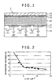
- Fig. 1 is a schematic sectional view illustrating the configuration of a liquid crystal display device 1 applicable in the present embodiment.
- the liquid crystal display device as a reflection type liquid crystal display device, comprises a Si (silicon) or other single crystal semiconductor substrate (Si driving circuit substrate 10) provided with light-reflecting electrodes 11 having a pixel structure, and a glass substrate 15 provided with a transparent electrode 14 and opposed thereto, and the two substrates are disposed opposite to each other, with Vertically aligned liquid crystals 20 sealed therebetween.
- the Si driving circuit substrate 10 has a structure in which driving circuits each composed of a transistor (a CMOS or an n channel MOS) and a capacitor are formed on a single crystal silicon substrate, and light-reflecting electrodes 11 composed of Al (aluminum), Ag (silver) or the like metallic film are formed thereon.
- the light-reflecting electrode 11 combines a light-reflecting film with an electrode for the voltage impressed on a liquid crystal.
- a dielectric multi-layer film may be formed for enhancing reflectance or as a protective film for the metallic surface.
- a liquid crystal alignment film 12 is formed between the light-reflecting electrodes 11 and the vertically aligned liquid crystals 20, and a liquid crystal alignment film 13 is formed between the transparent electrode 14 of the glass substrate 15 and the vertically aligned liquid crystals 20.
- the drive voltage can be made to be 5 to 6 V by controlling the refractive index anisotropy ⁇ n to a value of not less than 0.1.
- the adjustment by controlling only An leads to a limitation in selecting the materials.
- the present inventors have found out that the magnitude of dielectric constant anisotropy
- the response time is proportional to the square of the thickness of the crystal layer and is inversely proportional to the square of the drive voltage.
- Rise time: ⁇ on ⁇ ⁇ d 2 /[ ⁇ (0) ⁇ ⁇ ⁇ (V 2 -Vc 2 )]
- Fall time: ⁇ off ⁇ ⁇ d 2 /K ⁇ ⁇
- ⁇ is the viscosity of the liquid crystal
- ⁇ (0) is dielectric constant in vacuum
- V is the voltage impressed on the liquid crystal
- Vc the threshold voltage
- K is the elastic constant of the liquid crystal.
- the present embodiment shows that, in a liquid crystal device having a liquid crystal layer thickness of not more than 2.5 ⁇ m, which is thinner than a related-art device, the conditions for satisfying d ⁇ ⁇ n ⁇
- Fig. 2 is a diagram showing the relationship of the saturation voltage with the relational expression d ⁇ ⁇ n ⁇
- the relationship shown in this figure has been obtained assuming that the wavelength of light is 550 nm.
- the saturation voltage is not more than 4 V if d ⁇ ⁇ n ⁇
- FIG. 3 is a table for showing Examples of the present invention and Comparative Examples. Now, Comparative Examples and Examples will be sequentially described below.
- a vertically aligned liquid crystal display device was produced in the following manner.
- a glass substrate provided with a transparent electrode and an Si driving circuit substrate provided with Al electrodes were cleaned, were then introduced into a vapor deposition apparatus, and an SiO 2 film as a liquid crystal alignment film was formed thereon by skew vapor deposition at a vapor deposition angle in the range of 45° to 60°.
- the film thickness of the liquid crystal alignment film was controlled to 50 nm, and the pretilt angle of the liquid crystal was controlled to about 2.5°.
- both the substrates after the formation of the liquid crystal alignment film were adhered to each other with an interval of 2.5 ⁇ m therebetween by use of a seal member mixed with glass beads, and vertically aligned liquid crystals as follows were sealed therebetween, to produce a reflection type liquid crystal display device.
- 4.1, d ⁇ ⁇ n ⁇
- a vertically aligned liquid crystal display device was produced in the following manner.
- a glass substrate provided with a transparent electrode and an Si driving circuit substrate provided with Al electrodes were cleaned, were then introduced into a vapor deposition apparatus, and an SiO 2 film as a liquid crystal alignment film was formed thereon by skew vapor deposition at a vapor deposition angle in the range of 45° to 60°.
- the film thickness of the liquid crystal alignment film was controlled to 50 nm, and the pretilt angle of the liquid crystal was controlled to about 2.5°.
- both the substrates after the formation of the liquid crystal alignment film were adhered to each other with an interval of 1.9 ⁇ m therebetween by use of a seal member mixed with glass beads, and the vertically aligned liquid crystals described in Comparative Example A were sealed therebetween, to produce a reflection type liquid crystal display device.
- the liquid crystal used had d ⁇ ⁇ n ⁇
- a vertically aligned liquid crystal display device was produced in the following manner.
- a glass substrate provided with a transparent electrode and an Si driving circuit substrate provided with Al electrodes were cleaned, were then introduced into a vapor deposition apparatus, and an SiO 2 film as a liquid crystal alignment film was formed thereon by skew vapor deposition at a vapor deposition angle in the range of 45° to 60°.
- the film thickness of the liquid crystal alignment film was controlled to 50 nm, and the pretilt angle of the liquid crystal was controlled to about 2.5°.
- both the substrates after the formation of the liquid crystal alignment film were adhered to each other with an interval of 1.9 ⁇ m therebetween by use of a seal member mixed with glass beads, and vertically aligned liquid crystals as follows were sealed therebetween, to produce a reflection type liquid crystal display device.
- 5.0, d ⁇ ⁇ n ⁇
- a vertically aligned liquid crystal display device was produced in the following manner.
- a glass substrate provided with a transparent electrode and an Si driving circuit substrate provided with Al electrodes were cleaned, were then introduced into a vapor deposition apparatus, and an SiO 2 film as a liquid crystal alignment film was formed thereon by skew vapor deposition at a vapor deposition angle in the range of 45° to 60°.
- the film thickness of the liquid crystal alignment film was controlled to 50 nm, and the pretilt angle of the liquid crystal was controlled to about 2.5°.
- both the substrates after the formation of the liquid crystal alignment film were adhered to each other with an interval of 1.9 ⁇ m therebetween by use of a seal member mixed with glass beads, and vertically aligned liquid crystals as follows were sealed therebetween, to produce a reflection type liquid crystal display device.
- 4.0, d ⁇ n ⁇
- a vertically aligned liquid crystal display device was produced in the following manner.
- a glass substrate provided with a transparent electrode and an Si driving circuit substrate provided with A1 electrodes were cleaned, were then introduced into a vapor deposition apparatus, and an SiO 2 film as a liquid crystal alignment film was formed thereon by skew vapor deposition at a vapor deposition angle in the range of 45° to 60°.
- the film thickness of the liquid crystal alignment film was controlled to 50 nm, and the pretilt angle of the liquid crystal was controlled to about 2.5°.
- both the substrates after the formation of the liquid crystal alignment film were adhered to each other with an interval of 2.4 ⁇ m therebetween by use of a seal member mixed with glass beads, and vertically aligned liquid crystals as follows were sealed therebetween, to produce a reflection type liquid crystal display device.
- 7.0, d ⁇ ⁇ n ⁇
- a vertically aligned liquid crystal display device was produced in the following manner.
- a glass substrate provided with a transparent electrode and an Si driving circuit substrate provided with Al electrodes were cleaned, were then introduced into a vapor deposition apparatus, and an SiO 2 film as a liquid crystal alignment film was formed thereon by skew vapor deposition at a vapor deposition angle in the range of 45° to 60°.
- the film thickness of the liquid crystal alignment film was controlled to 50 nm, and the pretilt angle of the liquid crystal was controlled to about 2.5°.
- a vertically aligned liquid crystal display device was produced in the following manner.
- a glass substrate provided with a transparent electrode and an Si driving circuit substrate provided with Al electrodes were cleaned, were then introduced into a vapor deposition apparatus, and an SiO 2 film as a liquid crystal alignment film was formed thereon by skew vapor deposition at a vapor deposition angle in the range of 45° to 60°.
- the film thickness of the liquid crystal alignment film was controlled to 50 nm, and the pretilt angle of the liquid crystal was controlled to about 2.5°.
- both the substrates after the formation of the liquid crystal alignment film were adhered to each other with an interval of 1.9 ⁇ m therebetween by use of a seal member mixed with glass beads, and vertically aligned liquid crystals as shown in the following table were sealed therebetween, to produce a reflection type liquid crystal display device.
- 6.3, d ⁇ ⁇ n ⁇
- a vertically aligned liquid crystal display device was produced in the following manner.
- a glass substrate provided with a transparent electrode and an Si driving circuit substrate provided with Al electrodes were cleaned, were then introduced into a vapor deposition apparatus, and an SiO 2 film as a liquid crystal alignment film was formed thereon by skew vapor deposition at a vapor deposition angle in the range of 45° to 60°.
- the film thickness of the liquid crystal alignment film was controlled to 50 nm, and the pretilt angle of the liquid crystal was controlled to about 2.5°.
- a vertically aligned liquid crystal display device was produced in the following manner.
- a glass substrate provided with a transparent electrode and an Si driving circuit substrate provided with Al electrodes were cleaned, were then introduced into a vapor deposition apparatus, and an SiO 2 film as a liquid crystal alignment film was formed thereon by skew vapor deposition at a vapor deposition angle in the range of 45° to 60°.
- the film thickness of the liquid crystal alignment film was controlled to 50 nm, and the pretilt angle of the liquid crystal was controlled to about 2.5°.
- a vertically aligned liquid crystal display device was produced in the following manner.
- a glass substrate provided with a transparent electrode and an Si driving circuit substrate provided with Al electrodes were cleaned, were then introduced into a vapor deposition apparatus, and an SiO 2 film as a liquid crystal alignment film was formed thereon by skew vapor deposition at a vapor deposition angle in the range of 45° to 60°,
- the film thickness of the liquid crystal alignment film was controlled to 50 nm, and the pretilt angle of the liquid crystal was controlled to about 2.5°.
- both the substrates after the formation of the liquid crystal alignment film were adhered to each other with an interval of 1.9 or 2.5 ⁇ m therebetween by use of a seal member mixed with glass beads, and vertically aligned liquid crystals shown in the following table were sealed therebetween, to produce a reflection type liquid crystal display device.
- 2 6.14 to 10.7
- a saturation voltage (measured at 550 nm) 3.1 to 3.9 V.
- the saturation voltage can be made to be not more than 4 V when d ⁇ ⁇ n ⁇
- FIG. 4 is a diagram showing the relationship of the saturation voltage for R (RED) against d ⁇ ⁇ n ⁇
- the saturation voltage (RED) in Examples 2 above is 4.5 V
- the saturation voltage (RED) in Example 3 is 3.3 V
- the saturation voltage (RED) in Example 6 is 4.2 V
- the saturation voltage (RED) in Example 9 is 5.0 V
- the saturation voltage (RED) in Example 10 is 4.3 V
- the saturation voltage (RED) in Example 11 is 5.0 V
- the saturation voltage (RED) in Comparative Example B is 15 V
- the saturation voltage (RED) in Comparative Example C is 7 V
- the saturation voltage (RED) in Comparative Example D is 12 V.
- a threshold of the saturation voltage (RED) is in the vicinity of the position where the value of d ⁇ ⁇ n ⁇
- value of not less than 5.5 is necessary for satisfying d ⁇ ⁇ n ⁇
- the optical path difference at the time when the reflectance in the reflection type liquid crystal display device reached a maximum is one half (1/2) of the wavelength at that time. Since, in the reflection type liquid crystal display device, d can be deemed as doubled in view of the forward going and the returning, d ⁇ ⁇ n(eff) is ⁇ /4.
- ⁇ n(eff) is the effective value of ⁇ n, i.e., the actual refractive index anisotropy.
- ⁇ n is a physical value intrinsic of a liquid crystal material
- the refractive index anisotropy ⁇ n(eff) in use in an actual vertically aligned liquid crystal device is represented as follows. where n(//) is the refractive index in the major axis direction of the liquid crystal, n( ⁇ ) is the refractive index in the minor axis direction of the liquid crystal, and ⁇ is the tilt angle of liquid crystal molecules.
- a high light output can be obtained by setting the tilt angle ⁇ of the liquid crystal molecules used, i.e., the voltage for driving the reflection type liquid crystal device, so as to satisfy the condition for the reflectance in the reflection type liquid crystal device (ratio of outgoing light as opposed to incident light) to reach a maximum.
- ⁇ is the angle to which the liquid crystals are tilted upon application of a voltage
- the value of ⁇ can intrinsically range from 0° to 90°.
- ⁇ in an actual device is about 60° at maximum, even in the case of a liquid crystal material having, for example, a ⁇ n value of 0.1, ⁇ n(eff) in the actual device is no more than about 0.08 (80% of ⁇ n) at maximum.
- Fig. 5 is a schematic diagram showing an example of application of a reflection type liquid crystal display device according to the present embodiment to a projection system.
- the projection system 100 comprises a lamp light source 101, a lens unit 102, dichroic color separation filters 103, a dichroic mirror 110, total reflection mirror 108, 109, beam splitters 104r, 104g, 104b, reflection type liquid crystal display devices 1r, 1g, 1b, driving circuits 105r, 105g, 105b, a prism 106, and a projection lens 107.
- the lamp light source 101 outputs light containing three color components of R (RED), G (GREEN), and B (BLUE), and is composed, for example, a metal halide lamp, an extra-high pressure mercury lamp or the like.
- the lens unit 102 condenses the light outputted from the lamp light source 101 so that the reflection type liquid crystal display devices 1r, 1g, 1b are illuminated appropriately.
- the lens unit 102 may be configured together with a pair of fly eye lenses, for evening the output of light from the lamp light source 101.
- the dichroic color separation filter 103 and the dichroic mirror 110 separate the inputted light into predetermined color rays.
- the beam splitters 104r, 104g, 104b are devices for separating the polarized light components of the light by transmitting predetermined polarized light (for example, P polarized light) while reflecting light (for example, S polarized light orthogonal to the P polarized light) in the different polarization direction from that of the predetermined polarized light.
- the prism 106 is a device for composing the color rays incident from three directions and emitting the composed light, and is composed, for example, of a so-called cross-dichroic prism in which dichroic filters are disposed in an intersected manner.
- the light emitted from the lamp light source 101 is sent through the lens unit 102 to the dichroic color separation filter 103, where the light is separated into two directions as different color rays.
- the color rays thus separated into two directions are sent to display units composed of the reflection type liquid crystal display devices 1r, 1g, 1b corresponding to the three colors of R (RED), G (GREEN), and B (BLUE), by the total reflection mirrors 108, 109, the beam splitters 104r, 104g, 104b, the dichroic mirror 110, and the prism 106.
- the light from the lamp light source 101 is color-separated by the dichroic color separation filter 103, the color rays containing R (RED) and G (GREEN) component rays are reflected by the total reflection filter 108 to be supplied to the dichroic mirror 110, and R (RED) component ray obtained by color separation in the dichroic mirror 110 and transmitted is incident on the reflection type liquid crystal display device 1r corresponding to R (RED), through the beam splitter 104r.
- the light from the lamp light source 101 is color-separated by the dichroic color separation filter 103, the color rays containing R (RED) and G (GREEN) component rays are reflected by the total reflection mirror 108 to be supplied to the dichroic mirror 110, and the G (GREEN) component ray color-separated by the dichroic mirror 110 and reflected is incident on the reflection type liquid crystal display device 1g corresponding to G (GREEN), through the beam splitter 104g.
- the light from the lamp light source 101 is color-separated by the dichroic color separation filter 103, and the color ray containing B (BLUE) component ray is reflected by the total reflection mirror is incident on the reflection type liquid crystal display device 1b corresponding to B (BLUE), through the beam splitter 104b.
- the reflection type liquid crystal display devices 1r, 1g, 1b are driven respectively by the corresponding driving circuits 105r, 105g, 105b. Specifically, based on image signals corresponding respectively to the colors, a voltage is impressed on each pixel, the polarization planes of the polarized rays incident through the beam splitters 104r, 104g, 104b are optically rotated by the liquid crystal layer, and the rotatorily polarized light is reflected by the light reflecting electrode 11, before outgoing.
- the beam splitters 104r, 104g, 104b outputs predetermined polarized light components of the outgoing light to the prism 106 as image rays.
- the color image rays thus outputted are composed by the prism 106, and the composed light is sent to the projection lens 107.
- an image corresponding to the three colors of R (RED), G (GREEN), and B (BLUE) is projected on a screen (not shown), to be reproduced as a color image.
- the above-described reflection type liquid crystal display devices 1r, 1g, 1b are used in correspondence with the R (RED), G (GREEN), and B (BLUE) colors, so that the devices can be driven at a high response speed, a high contrast, and a low voltage.
- the reflection type liquid crystal display devices 1r, 1g, 1b for R (RED), G (GREEN), and B (BLUE) differ in saturation voltage
- the present embodiment is characterized in that the driving circuits 105r, 105g, 105b for driving the reflection type liquid crystal display devices 1r, 1g, 1b are different in maximum drive voltage.
- the saturation voltage differs depending on the wavelength.
- the saturation voltage therefor is not more than 4 V
- the saturation voltage therefor is 5 to 6 V. Therefore, depending on the difference in saturation voltage, the maximum drive voltages given from the driving circuits 105r, 105g, 105b are varied on the basis of each of the reflection type liquid crystal display devices 1r, 1g, 1b.
- each of the driving circuits 105r, 105g, 105b is so configured that the maximum drive voltage can be variably set so as to make it possible to correspond to the saturation voltage for each color.
- the maximum drive voltage can be variably set so as to make it possible to correspond to the saturation voltage for each color.
- the reflection type liquid crystal display device is applicable not only to the above-described projection system but also to various display apparatuses such as a display of an electronic apparatus for displaying an image directly, without projection onto a screen.
Landscapes
- Physics & Mathematics (AREA)
- Nonlinear Science (AREA)
- Engineering & Computer Science (AREA)
- Multimedia (AREA)
- Signal Processing (AREA)
- Chemical & Material Sciences (AREA)
- Crystallography & Structural Chemistry (AREA)
- General Physics & Mathematics (AREA)
- Optics & Photonics (AREA)
- Liquid Crystal (AREA)
- Projection Apparatus (AREA)
Applications Claiming Priority (2)
| Application Number | Priority Date | Filing Date | Title |
|---|---|---|---|
| JP2004061855 | 2004-03-05 | ||
| JP2004061855 | 2004-03-05 |
Publications (2)
| Publication Number | Publication Date |
|---|---|
| EP1571853A2 true EP1571853A2 (de) | 2005-09-07 |
| EP1571853A3 EP1571853A3 (de) | 2005-11-09 |
Family
ID=34747687
Family Applications (1)
| Application Number | Title | Priority Date | Filing Date |
|---|---|---|---|
| EP05004578A Ceased EP1571853A3 (de) | 2004-03-05 | 2005-03-02 | Reflektive Flüssigkristallanzeige und Projektionsapparat |
Country Status (5)
| Country | Link |
|---|---|
| US (1) | US8462299B2 (de) |
| EP (1) | EP1571853A3 (de) |
| KR (1) | KR101096410B1 (de) |
| CN (1) | CN1664660B (de) |
| TW (1) | TW200606536A (de) |
Families Citing this family (9)
| Publication number | Priority date | Publication date | Assignee | Title |
|---|---|---|---|---|
| US8427409B2 (en) * | 2007-03-28 | 2013-04-23 | Seiko Epson Corporation | Projector |
| US8339563B2 (en) * | 2009-09-21 | 2012-12-25 | Shanghai Lexvu Opto Microelectronics Technology Co., Ltd | Liquid crystal imager and method of making same |
| JP2013015815A (ja) * | 2011-06-06 | 2013-01-24 | Seiko Epson Corp | 投射型表示装置および光学ユニット |
| KR20150049630A (ko) | 2013-10-30 | 2015-05-08 | 삼성디스플레이 주식회사 | 표시 장치 |
| CN104460135B (zh) * | 2014-12-22 | 2019-01-15 | 厦门天马微电子有限公司 | 一种显示面板及显示装置 |
| US11656511B2 (en) * | 2020-10-23 | 2023-05-23 | Seurat Technologies, Inc. | Laser damage hardening of light modulator components for use with high optical fluence systems |
| CN107632447A (zh) * | 2017-09-26 | 2018-01-26 | 京东方科技集团股份有限公司 | 显示面板、显示装置及其控制方法 |
| CN114935789B (zh) * | 2022-05-19 | 2024-05-17 | 西安中科微星光电科技有限公司 | 一种窄带滤光片及其制备方法 |
| CN116577948A (zh) * | 2023-05-31 | 2023-08-11 | 汕头超声显示器技术有限公司 | 一种液晶后视镜 |
Family Cites Families (20)
| Publication number | Priority date | Publication date | Assignee | Title |
|---|---|---|---|---|
| JPH031285A (ja) | 1989-05-30 | 1991-01-07 | Nec Corp | バーコード自動読取方式 |
| JPH0667173A (ja) * | 1992-08-19 | 1994-03-11 | Sharp Corp | 液晶表示装置 |
| GB2314642A (en) * | 1996-06-26 | 1998-01-07 | Sharp Kk | Twisted nematic liquid crystal device |
| JPH10111513A (ja) * | 1996-10-04 | 1998-04-28 | Sony Corp | ゲストホスト液晶表示装置 |
| US7034785B2 (en) * | 1997-11-20 | 2006-04-25 | Sanyo Electric Co., Ltd. | Color liquid crystal display |
| US6067142A (en) * | 1999-01-27 | 2000-05-23 | International Business Machines Corporation | Vertically aligned pi-cell LCD having on-state with mid-plane molecules perpendicular to the substrates |
| JP3910370B2 (ja) * | 2000-02-08 | 2007-04-25 | シャープ株式会社 | 液晶表示デバイス |
| FR2808891B1 (fr) * | 2000-05-12 | 2003-07-25 | Nemoptic | Dispositif bistable d'affichage en reflexion |
| US6836309B2 (en) * | 2000-11-30 | 2004-12-28 | Hana Microdisplay Technologies, Inc. | High contrast reflective light valve |
| JP2002268066A (ja) | 2001-03-07 | 2002-09-18 | Seiko Epson Corp | 液晶装置および投射型液晶装置並びに電子機器 |
| JP2002287149A (ja) | 2001-03-22 | 2002-10-03 | Seiko Epson Corp | 液晶装置及び電子機器並びに投射型液晶装置 |
| JP2002341320A (ja) * | 2001-05-15 | 2002-11-27 | Fuji Photo Film Co Ltd | 液晶表示装置および光学積層体 |
| US7106401B2 (en) * | 2001-06-26 | 2006-09-12 | Sony Corporation | Reflex liquid crystal display device, display apparatus, projection optical system, and projection display system |
| JP3758654B2 (ja) | 2001-06-26 | 2006-03-22 | ソニー株式会社 | プロジェクション光学システム及びプロジェクションディスプレイシステム |
| CN1267777C (zh) * | 2001-06-26 | 2006-08-02 | 索尼公司 | 反射液晶显示装置、显示设备、投影光学系统和投影显示系统 |
| JP3758612B2 (ja) * | 2001-06-26 | 2006-03-22 | ソニー株式会社 | 反射型液晶表示素子、表示装置、プロジェクション光学システム、及びプロジェクションディスプレイシステム |
| JP4689900B2 (ja) * | 2001-08-22 | 2011-05-25 | Nec液晶テクノロジー株式会社 | 液晶表示装置 |
| JP3949924B2 (ja) * | 2001-10-15 | 2007-07-25 | シャープ株式会社 | 反射型液晶表示装置用基板およびそれを用いた反射型液晶表示装置 |
| KR20040002155A (ko) * | 2002-06-29 | 2004-01-07 | 비오이 하이디스 테크놀로지 주식회사 | 수직 배향 모드 액정표시장치 |
| US20040165128A1 (en) * | 2003-02-26 | 2004-08-26 | Three-Five Systems, Inc. | Vertically aligned nematic mode liquid crystal display having large tilt angles and high contrast |
-
2005
- 2005-03-01 US US11/069,369 patent/US8462299B2/en not_active Expired - Fee Related
- 2005-03-02 EP EP05004578A patent/EP1571853A3/de not_active Ceased
- 2005-03-04 TW TW094106667A patent/TW200606536A/zh not_active IP Right Cessation
- 2005-03-04 KR KR1020050018009A patent/KR101096410B1/ko not_active Expired - Fee Related
- 2005-03-04 CN CN2005100677291A patent/CN1664660B/zh not_active Expired - Fee Related
Non-Patent Citations (1)
| Title |
|---|
| WU, SHIN-TSON: "Reflective Liquid Crystal Displays", 2001, JOHN WILEY & SONS LTD., Chichester, UK, ISBN: 0-471-49611-1 * |
Also Published As
| Publication number | Publication date |
|---|---|
| EP1571853A3 (de) | 2005-11-09 |
| KR101096410B1 (ko) | 2011-12-21 |
| CN1664660B (zh) | 2010-06-16 |
| TW200606536A (en) | 2006-02-16 |
| CN1664660A (zh) | 2005-09-07 |
| US8462299B2 (en) | 2013-06-11 |
| US20050231662A1 (en) | 2005-10-20 |
| TWI293393B (de) | 2008-02-11 |
| KR20060043389A (ko) | 2006-05-15 |
Similar Documents
| Publication | Publication Date | Title |
|---|---|---|
| KR100893241B1 (ko) | 대체된 편광판을 가진 마이크로디스플레이 시스템 | |
| JP3144132B2 (ja) | 液晶表示装置およびそれを用いた投写型表示装置 | |
| US7982848B2 (en) | Variable transmission light quantity element with dielectric layers and projection display | |
| US7903212B2 (en) | Reflex liquid crystal display device, display apparatus, projection optical system, and projection display system | |
| US20080018630A1 (en) | Liquid crystal display device, liquid crystal display and method of driving liquid crystal display device | |
| JP2005156717A (ja) | 液晶表示素子及び液晶表示装置 | |
| US20080117385A1 (en) | Liquid crystal device and projector having the same | |
| US8462299B2 (en) | Reflection type liquid crystal display device, display apparatus, and projection system | |
| TW526382B (en) | Optical display system including an achromatized ferroelectric light valve | |
| EP1515569A1 (de) | Flüssigkristallprojektor | |
| CN1620822A (zh) | 投影显示系统 | |
| JP4029786B2 (ja) | 液晶表示素子及び液晶表示装置 | |
| JP3758612B2 (ja) | 反射型液晶表示素子、表示装置、プロジェクション光学システム、及びプロジェクションディスプレイシステム | |
| US7440059B2 (en) | Reflection type liquid crystal display element and liquid crystal display unit | |
| JP7810009B2 (ja) | 液晶装置、表示装置、光変調モジュール、および液晶装置の制御方法 | |
| JP2005284265A (ja) | 反射型液晶表示素子、表示装置ならびにプロジェクションシステム | |
| KR20040046137A (ko) | 반사형 액정 디스플레이를 구비한 프로젝션 시스템 | |
| JP3758654B2 (ja) | プロジェクション光学システム及びプロジェクションディスプレイシステム | |
| JP4143922B2 (ja) | プロジェクションディスプレイシステム | |
| US20040196418A1 (en) | Reflex liquid crystal display device, display apparatus, projection optical system, and projection display system | |
| JP2833134B2 (ja) | 液晶駆動装置および液晶パネルの駆動方法 | |
| WO2005060268A1 (en) | Brightness regulation in lcd projection systems | |
| KR20000071651A (ko) | 액정 표시 소자 및 이를 이용한 액정 표시 장치 | |
| JPH05341260A (ja) | 液晶表示装置 | |
| KR20040069578A (ko) | 반사형 액정 디스플레이와 이를 이용한 프로젝션 시스템 |
Legal Events
| Date | Code | Title | Description |
|---|---|---|---|
| PUAI | Public reference made under article 153(3) epc to a published international application that has entered the european phase |
Free format text: ORIGINAL CODE: 0009012 |
|
| AK | Designated contracting states |
Kind code of ref document: A2 Designated state(s): AT BE BG CH CY CZ DE DK EE ES FI FR GB GR HU IE IS IT LI LT LU MC NL PL PT RO SE SI SK TR |
|
| AX | Request for extension of the european patent |
Extension state: AL BA HR LV MK YU |
|
| PUAL | Search report despatched |
Free format text: ORIGINAL CODE: 0009013 |
|
| AK | Designated contracting states |
Kind code of ref document: A3 Designated state(s): AT BE BG CH CY CZ DE DK EE ES FI FR GB GR HU IE IS IT LI LT LU MC NL PL PT RO SE SI SK TR |
|
| AX | Request for extension of the european patent |
Extension state: AL BA HR LV MK YU |
|
| 17P | Request for examination filed |
Effective date: 20060327 |
|
| AKX | Designation fees paid |
Designated state(s): DE FR GB |
|
| STAA | Information on the status of an ep patent application or granted ep patent |
Free format text: STATUS: THE APPLICATION HAS BEEN REFUSED |
|
| 18R | Application refused |
Effective date: 20120112 |