EP1571471A2 - Optische Anordnung mit beweglichem Reflektor - Google Patents
Optische Anordnung mit beweglichem Reflektor Download PDFInfo
- Publication number
- EP1571471A2 EP1571471A2 EP05004311A EP05004311A EP1571471A2 EP 1571471 A2 EP1571471 A2 EP 1571471A2 EP 05004311 A EP05004311 A EP 05004311A EP 05004311 A EP05004311 A EP 05004311A EP 1571471 A2 EP1571471 A2 EP 1571471A2
- Authority
- EP
- European Patent Office
- Prior art keywords
- optical
- mirror
- reflecting surface
- reflecting
- plane
- Prior art date
- Legal status (The legal status is an assumption and is not a legal conclusion. Google has not performed a legal analysis and makes no representation as to the accuracy of the status listed.)
- Withdrawn
Links
Images






Classifications
-
- G—PHYSICS
- G02—OPTICS
- G02B—OPTICAL ELEMENTS, SYSTEMS OR APPARATUS
- G02B6/00—Light guides; Structural details of arrangements comprising light guides and other optical elements, e.g. couplings
- G02B6/24—Coupling light guides
- G02B6/26—Optical coupling means
- G02B6/35—Optical coupling means having switching means
- G02B6/351—Optical coupling means having switching means involving stationary waveguides with moving interposed optical elements
- G02B6/3512—Optical coupling means having switching means involving stationary waveguides with moving interposed optical elements the optical element being reflective, e.g. mirror
- G02B6/352—Optical coupling means having switching means involving stationary waveguides with moving interposed optical elements the optical element being reflective, e.g. mirror the reflective optical element having a shaped reflective surface, e.g. a reflective element comprising several reflective surfaces or facets that function together
-
- G—PHYSICS
- G02—OPTICS
- G02B—OPTICAL ELEMENTS, SYSTEMS OR APPARATUS
- G02B26/00—Optical devices or arrangements for the control of light using movable or deformable optical elements
- G02B26/08—Optical devices or arrangements for the control of light using movable or deformable optical elements for controlling the direction of light
- G02B26/0816—Optical devices or arrangements for the control of light using movable or deformable optical elements for controlling the direction of light by means of one or more reflecting elements
- G02B26/0833—Optical devices or arrangements for the control of light using movable or deformable optical elements for controlling the direction of light by means of one or more reflecting elements the reflecting element being a micromechanical device, e.g. a MEMS mirror, DMD
- G02B26/0841—Optical devices or arrangements for the control of light using movable or deformable optical elements for controlling the direction of light by means of one or more reflecting elements the reflecting element being a micromechanical device, e.g. a MEMS mirror, DMD the reflecting element being moved or deformed by electrostatic means
-
- G—PHYSICS
- G02—OPTICS
- G02B—OPTICAL ELEMENTS, SYSTEMS OR APPARATUS
- G02B6/00—Light guides; Structural details of arrangements comprising light guides and other optical elements, e.g. couplings
- G02B6/24—Coupling light guides
- G02B6/26—Optical coupling means
- G02B6/264—Optical coupling means with optical elements between opposed fibre ends which perform a function other than beam splitting
- G02B6/266—Optical coupling means with optical elements between opposed fibre ends which perform a function other than beam splitting the optical element being an attenuator
-
- G—PHYSICS
- G02—OPTICS
- G02B—OPTICAL ELEMENTS, SYSTEMS OR APPARATUS
- G02B6/00—Light guides; Structural details of arrangements comprising light guides and other optical elements, e.g. couplings
- G02B6/24—Coupling light guides
- G02B6/26—Optical coupling means
- G02B6/35—Optical coupling means having switching means
- G02B6/351—Optical coupling means having switching means involving stationary waveguides with moving interposed optical elements
-
- G—PHYSICS
- G02—OPTICS
- G02B—OPTICAL ELEMENTS, SYSTEMS OR APPARATUS
- G02B6/00—Light guides; Structural details of arrangements comprising light guides and other optical elements, e.g. couplings
- G02B6/24—Coupling light guides
- G02B6/26—Optical coupling means
- G02B6/35—Optical coupling means having switching means
- G02B6/351—Optical coupling means having switching means involving stationary waveguides with moving interposed optical elements
- G02B6/3512—Optical coupling means having switching means involving stationary waveguides with moving interposed optical elements the optical element being reflective, e.g. mirror
- G02B6/3514—Optical coupling means having switching means involving stationary waveguides with moving interposed optical elements the optical element being reflective, e.g. mirror the reflective optical element moving along a line so as to translate into and out of the beam path, i.e. across the beam path
-
- G—PHYSICS
- G02—OPTICS
- G02B—OPTICAL ELEMENTS, SYSTEMS OR APPARATUS
- G02B6/00—Light guides; Structural details of arrangements comprising light guides and other optical elements, e.g. couplings
- G02B6/24—Coupling light guides
- G02B6/26—Optical coupling means
- G02B6/35—Optical coupling means having switching means
- G02B6/3564—Mechanical details of the actuation mechanism associated with the moving element or mounting mechanism details
- G02B6/3568—Mechanical details of the actuation mechanism associated with the moving element or mounting mechanism details characterised by the actuating force
- G02B6/357—Electrostatic force
-
- G—PHYSICS
- G02—OPTICS
- G02B—OPTICAL ELEMENTS, SYSTEMS OR APPARATUS
- G02B6/00—Light guides; Structural details of arrangements comprising light guides and other optical elements, e.g. couplings
- G02B6/24—Coupling light guides
- G02B6/26—Optical coupling means
- G02B6/35—Optical coupling means having switching means
- G02B6/3594—Characterised by additional functional means, e.g. means for variably attenuating or branching or means for switching differently polarized beams
-
- G—PHYSICS
- G02—OPTICS
- G02B—OPTICAL ELEMENTS, SYSTEMS OR APPARATUS
- G02B6/00—Light guides; Structural details of arrangements comprising light guides and other optical elements, e.g. couplings
- G02B6/24—Coupling light guides
- G02B6/26—Optical coupling means
- G02B6/35—Optical coupling means having switching means
- G02B6/3596—With planar waveguide arrangement, i.e. in a substrate, regardless if actuating mechanism is outside the substrate
Definitions
- the present invention relates to an optical device for regulating the power of light propagating from a first optical path to a second optical path, and a movable reflector used in the optical device.
- Optical communication is often implemented using optical devices for regulating the power of optical signals, e.g., variable optical attenuators and optical switches.
- optical devices for regulating the power of optical signals, e.g., variable optical attenuators and optical switches.
- An example of such optical devices is disclosed in C. Marxer et al., "Micro-Opto-Mechanical 2x2 Switch for Single Mode Fibers based on Plasma-Etched Silicon Mirror and Electrostatic Actuation" (preceding 11th IEEE Workshop on Micro-Electro-Mechanical System, 1998, pp233-237).
- a mirror is disposed on an optical path between two optical waveguides and the mirror is moved to change the quantity of the reflected light, thereby regulating the power of light propagating from one optical waveguide to another optical waveguide.
- Fig. 1 is a schematic plan view showing an example of a variable optical attenuator using a mirror.
- the variable optical attenuator 50 has a Planar Lightwave Circuit (PLC) 10, a mirror 20, and a mirror driver device 30.
- Optical waveguides 11 and 12 in the PLC 10 have their respective ends placed in mirror symmetry with respect to a plane 13. These ends have their respective end faces 11a and 12a aligned on a single plane.
- the mirror 20 has a reflecting surface 20a parallel to these end faces 11a and 12a.
- the mirror driver device 30 is able to move the mirror 20 along directions indicated by arrows 32 and 33.
- When light from the optical waveguide 11 is incident onto the reflecting surface 20a, it is reflected toward the optical waveguide 12. This causes the light to propagate from the optical waveguide 11 to the optical waveguide 12.
- the light from the optical waveguide 11 is not incident onto the reflecting surface 20a, the light does not enter the optical waveguide 12.
- the reflecting surface 20a has an edge 20b that moves across the plane 13 with movement of the mirror 20.
- incident light is scattered into various directions by virtue of diffraction. For this reason, part of the light from the optical waveguide 11 is fed back to the optical waveguide 11 to propagate again in the optical waveguide 11. This light is optical feedback to the optical waveguide 11.
- This optical feedback can distort the waveform of the signal light propagating in the optical waveguide 11 and cause a communication error.
- an object of the present invention to reduce the optical feedback to a first optical path in an optical device for regulating the power of light propagating from the first optical path to a second optical path.
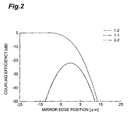
- Fig. 2 shows the relationship between the position of the mirror edge 20b and coupling efficiency in the variable optical attenuator 50 shown in Fig. 1.
- the edge 20b is located on the plane 13 between the optical waveguides 11 and 12.
- a solid line represents the coupling efficiency of light traveling from the optical waveguide 11 to the optical waveguide 12
- a chain line the coupling efficiency of light fed from the optical waveguide 11 back to the optical waveguide 11
- a chain double-dashed line the coupling efficiency of light fed from the optical waveguide 12 back to the optical waveguide 12.
- the chain line and the chain double-dashed line overlap each other.
- the variable optical attenuator 50 demonstrates the large coupling efficiency of optical feedback to the optical waveguides 11 and 12. Therefore, the waveform of signal light in the optical waveguides is relatively likely to be distorted.
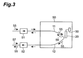
- a conceivable method of preventing the distortion of the waveform of signal light is to connect isolators 51 and 52 to the respective optical waveguides 11 and 12, as shown in Fig. 3.
- Signal light 55 propagating in the optical waveguide 11 is reflected by the mirror 20 and is then incident into the optical waveguide 12 to propagate in the optical waveguide 12.
- Optical feedback 56 to the optical waveguide 11, caused by scattering at the edge part 20b of the mirror 20, is cut off by the isolator 51 connected to the optical waveguide 11.
- the isolator 52 connected to the optical waveguide 12 cuts off optical feedback 57 from an external device connected to the variable optical attenuator 50 to prevent incidence thereof into the variable optical attenuator 50. Therefore, it is also feasible to prevent occurrence of optical feedback from the optical waveguide 12 to the optical waveguide 12.
- a typical tolerance of coupling efficiency of optical feedback is -45 dB, and tolerances differ according to systems using the variable optical attenuator.
- isolators as described above makes it feasible to prevent the influence of optical feedback on the signal light in the optical communication system using the variable optical attenuator.
- the need for connection of the isolators to the optical waveguides leads to making construction of the system more complex and increasing the production cost of the system.
- the Inventors invented another optical device and mirror capable of reducing the optical feedback.
- the present invention relates to an optical device comprising a first optical path having a first optical axis; a second optical path having a second optical axis not parallel to the first optical axis; and a mirror adapted to move across a bisector of an angle between the first optical axis and the second optical axis.
- the mirror has a surface including a reflecting portion for, when receiving light from the first optical path, reflecting the light toward the second optical path.
- the reflecting portion may have an edge including a linear portion placed on a plane substantially perpendicular to the bisector.
- the linear portion may be inclined relative to a normal to a plane including the first and second optical axes.
- An acute angle between the linear portion and the normal is preferably not less than 5°.
- the reflecting portion may have an edge including a curved portion placed on a plane substantially perpendicular to the bisector.
- the distance between the two X coordinates where the value of function Rav(X) varies from 10% to 90% is preferably not less than 3% of a mode field diameter in the X-direction of the light incident from the first optical path to the reflecting portion.
- the optical device in accordance with the present invention may further comprise at least either an optical waveguide optically coupled to the first optical path or an optical waveguide optically coupled to the second optical path.
- the optical waveguides may be planar waveguides or optical fibers.
- the present invention relates to a movable reflector comprising a reflecting surface, and a driver device capable of moving the reflecting surface along a predetermined moving path.
- the moving path extends in parallel with a plane substantially perpendicularly traversing the reflecting surface.
- the reflecting surface has an edge adapted to move while intersecting the plane as the reflecting surface moves along the moving path.
- the edge may include a linear portion inclined relative to a normal to the plane. An acute angle between the linear portion and the normal is preferably not less than 5°.
- the edge may include a curved portion.
- Fig. 1 is a schematic plan view showing an example of a variable optical attenuator.
- Fig. 2 is a graph showing the relationship between position of an edge of a mirror shown in Fig. 1, and coupling efficiency.
- Fig. 3 is a schematic diagram showing one method of reducing optical feedback.
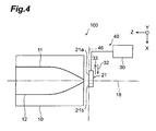
- Fig. 4 is a schematic plan view showing a variable optical attenuator of a first embodiment.
- Fig. 5 is a schematic perspective view showing a mirror in the first embodiment.
- Fig. 6 is a view showing a reflecting surface of the mirror from an angle different from that in Fig. 5.
- Fig. 7 is a schematic perspective view showing an enlarged view of the mirror shown in Fig. 1.
- Fig. 8 is a graph showing coupling efficiencies of optical feedback according to edge angles.
- Fig. 9 is a schematic perspective view showing a mirror in a second embodiment.
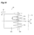
- Fig. 10 is a schematic plan view showing a mirror in a third embodiment.
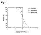
- Fig. 11 is a chart showing function Rav(X).
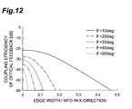
- Fig. 12 is a graph showing coupling efficiencies of optical feedback according to (edge width / MFD in X-directional).
- Fig. 13 is a schematic perspective view showing examples of the mirror in the third embodiment.
- Fig. 4 is a schematic plan view showing an optical device of the first embodiment.
- This optical device is a variable optical attenuator 100.
- the variable optical attenuator 100 has a Planar Lightwave Circuit (PLC) 10, a mirror 21, and a mirror driver device 30.
- PLC Planar Lightwave Circuit
- the mirror 21 and the mirror driver device 30 constitute a movable reflector 40.
- the PLC 10 has two optical waveguides 11 and 12.
- the optical waveguides 11 and 12 are planar waveguides extending in parallel to the plane of Fig. 4.
- the optical waveguides 11 and 12 are made, for example, of silica glass.
- the ends of the optical waveguides 11 and 12 on the side near the mirror 21 may intersect and overlap with each other, or may be separated from each other.
- the mirror 21 is an optical reflector having a reflecting surface 21a.
- the reflecting surface 21a is substantially flat and has an extremely high reflectance (e.g., 90% or more) for light of a predetermined wavelength propagating in the optical waveguides 11 and 12.
- the reflecting surface 21a has a substantially uniform reflectance.
- the reflecting surface 21a is provided on a surface of the mirror 21 and extends in the direction perpendicular to the plane of Fig. 4.
- the mirror 21 moves so that the reflecting surface 21a faces the end faces of the optical waveguides 11 and 12.
- the clearance between the reflecting surface 21a and these end faces may be filled with a refractive-index matching material. The details of the mirror 21 will be described later.
- the mirror driver device 30 moves the mirror 21 substantially in parallel with the ZX plane, as indicated by arrows 32 and 33.
- the reflecting surface 21a of the mirror 21 moves along a moving path 46.
- the movement of the mirror 21 is reversible.
- the moving path 46 extends in parallel with a plane (e.g., the plane of Fig. 4) substantially perpendicularly traversing the reflecting surface 21a.
- the moving path 46 is of a linear shape extending substantially in the X-direction.
- the reflecting surface 21a moves substantially in parallel with the end faces of the optical waveguides 11 and 12, as indicated by arrows 32 and 33.
- An example of the mirror driver device 30 is an electrostatic actuator as described in C. Marxer et al. mentioned above.
- the moving path 46 may also be of a curved shape. If the radius of curvature of the moving path 46 is sufficiently large, the reflecting surface 21a can be moved substantially in the X-direction in the region near the end faces of the optical waveguides 11 and 12.
- Fig. 4 An XYZ orthogonal coordinate system is depicted in Fig. 4 for convenience' sake of description.
- the X-axis extends along an intersecting line between the reflecting surface 21a and the plane including both the optical axes of the waveguides 11 and 12.
- the Y-axis extends perpendicularly to the X-axis in the plane perpendicular to a bisector of an angle between the two optical axes of the waveguides 11 and 12.
- the Z-axis extends in parallel with the bisector.
- Fig. 5 is a schematic perspective view showing the mirror 21.
- Fig. 6 is a view showing the reflecting surface 21a of the mirror 21 from an angle different from that in Fig. 5.
- the variable optical attenuator 100 has optical paths 26 and 27 for feeding light from the optical waveguide 11 via the mirror 21 to the optical waveguide 12.
- the optical paths 26 and 27 are optically coupled to the optical waveguides 11 and 12, respectively.
- the reflecting surface 21a of the mirror 21 moves so as to intersect the optical path 26.
- the optical paths 26 and 27 extend between the reflecting surface 21a and the end faces of the optical waveguides 11 and 12.
- Light 41 emerging from the optical waveguide 11 travels on the optical path 26 toward the mirror 21, and is reflected on the reflecting surface 21a to travel on the optical path 27 toward the optical waveguide 12.
- the optical paths 26 and 27 have their respective optical axes 16 and 17.
- the optical axes 16 and 17 are placed on a plane parallel to the plane of Fig. 4.
- the optical axes 16 and 17 are not parallel to each other, and intersect at an angle ⁇ .
- a bisector 18 of the angle ⁇ extends on the plane including the optical axes 16 and 17.
- Numeral 14 in Fig. 5 represents the plane including the optical axes 16 and 17.
- the plane 14 will be referred to hereinafter as a reference plane.
- the reference plane 14 is substantially parallel to the moving path 46 of the reflecting surface 21a and substantially perpendicularly traverses the reflecting surface 21a.
- the reflecting surface 21a of the mirror 21 is trapezoidal.
- the reflecting surface 21a has a linear edge 21b arranged to move so as to pass across the bisector 18 with movement of the mirror 21.
- the edge 21b moves while intersecting the reference plane 14 as the reflecting surface 21a moves along the moving path 46.
- the reflecting surface 21a and the edge 21b are located substantially on the XY plane.
- the bisector 18 is parallel to the Z-axis, as described above. Therefore, the edge 21b is located on a plane substantially perpendicular to the bisector 18.
- the edge 21b is inclined relative to a normal 15 to the reference plane 14 and makes an acute angle ⁇ with the normal 15.
- the reflecting surface 21a and the edge 21b are preferably perfectly perpendicular to the bisector 18.
- an angle between a projected line of the bisector 18 onto the reflecting surface 21a and the bisector 18 is within the range of 85° to 90°, and more preferably within the range of 89° to 90°.
- the reflecting surface 21a When receiving from the optical waveguide 11 the light 41 traveling along the optical axis 16 of the optical path 26, the reflecting surface 21a reflects the light 41 along the optical axis 17 of the optical path 27. In consequence, the light 41 from the optical waveguide 11 is incident along the optical axis 17 into the optical waveguide 12 and then propagates in the optical waveguide 12. On the other hand, if the light from the optical waveguide 11 does not impinge on the reflecting surface 21a, the light is not incident to the optical waveguide 12.
- Fig. 6 shows an enlarged view of a cross section of beam 44 of incident light 41.
- the incident light is scattered at the edge 21b by virtue of diffraction. Part of the scattered light is coupled to the optical waveguide 12 and propagates in the optical waveguide 12.
- the mirror 21 is moved in the direction of arrow 32 from the position shown in Fig. 6, the incident light comes to be reflected by a narrower region on the reflecting surface 21a, so as to decrease the coupling efficiency from the optical waveguide 11 to the optical waveguide 12.
- the mirror 21 is moved in the direction of arrow 33 from the position shown in Fig.
- the incident light comes to be reflected by a wider region on the reflecting surface 21a, so as to increase the coupling efficiency from the optical waveguide 11 to the optical waveguide 12. Therefore, the power of light propagating from the optical waveguide 11 to the optical waveguide 12 can be varied according to the movement of the mirror 21. This is the principle of the operation of the variable optical attenuator 100.
- the optical feedback is reduced by the inclination of the edge 21b relative to the normal 15 to the reference plane 14.
- the reduction of optical feedback by the mirror 21 in the present embodiment will be described below in comparison with the mirror 20 shown in Fig. 1, with reference to Figs. 5 and 7.
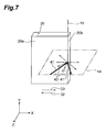
- Fig. 7 is a schematic perspective view showing the mirror 20 shown in Fig. 1.
- the reflecting surface 20a of the mirror 20 has an edge 20b.
- the edge 20b is a linear portion parallel to the normal 15 to the reference plane 14. Namely, the edge 20b is normal to the reference plane 14.
- the edge 20b is normal to the reference plane 14.
- the reason why no scattered light appears outside the plane 14 is that light components reflected by the portion of the reflecting surface 20a located on the upper side of the reference plane 14 and light components reflected by the portion of the reflecting surface 20a located on the lower side of the reference plane 14 cancel each other according to the Huygens' principle.
- part of scattered light 43 is relatively easily coupled with the optical waveguide 11 having the optical axis 16 on the same plane 14. The optical feedback to the optical waveguide 11 is induced in this manner.
- the mirror 21 of the present embodiment has the edge 21b inclined relative to the normal 15 to the reference plane 14, as shown in Fig. 5. Therefore, the reference plane 14 is not perpendicular to the edge 21b. For this reason, even if light is incident to the edge 21b along the optical axis 16 on the reference plane 14, optical scattering occurs within a plane not parallel to the reference plane 14. This results in decreasing the coupling efficiency of the scattered light to the optical waveguide 11 and thus decreasing the optical feedback to the optical waveguide 11.
- Fig. 8 shows the relationship between the inclination angle ⁇ of the edge 21b and the coupling efficiency of the optical feedback to the optical waveguide 11, for various values of the intersecting angle ⁇ between the optical axes 16 and 17.
- the incident light 41 is a beam having the wavelength of 1.55 ⁇ m in vacuum and having a Gaussian distribution with the center on the optical axis 16.
- the lateral MFD (mode field diameter) of incident light 41 is 20 ⁇ m and the vertical MFD 10 ⁇ m.
- the lateral direction and the vertical direction herein are defined as the major-axis direction and the minor-axis direction of elliptical section 44 of the incident light beam shown in Fig.
- the coupling efficiency of the optical feedback decreases as the inclination angle ⁇ of the edge 21b increase, under all the values of ⁇ .
- the larger the angle ⁇ the greater the effect of decreasing the coupling efficiency.
- ⁇ is 45° or more, the coupling efficiency of the optical feedback can be greatly suppressed to -40 dB or less under the inclination angle ⁇ of 5° or more.
- the angle between the end faces of the optical waveguides 11 and 12 facing the mirror 21 is determined according to the angle ⁇ between the optical axes 16 and 17.
- the curvature of the optical waveguides 11 and 12 tends to be large if ⁇ is large.
- light can leak in the curved portions of the optical waveguides 11 and 12, so as to raise the risk of occurrence of loss.
- an appropriate range of the angle ⁇ is 30° or less, and the inclination angle ⁇ of the edge 21b is preferably 10° or more.
- the inclination angle ⁇ is preferably 75° or less. Increase of the angle ⁇ will also result in increase of the moving distance of the reflecting surface 21a necessary for changing the power of light propagating from the optical waveguide 11 to the optical waveguide 12 by a predetermined amount. Therefore, a too large angle ⁇ will make it difficult to downsize the variable optical attenuator 100.
- the length of the edge 21b is preferably larger than the MFD of the incident light 41 in the direction along the edge 21b.
- Fig. 9 is a schematic perspective view showing a mirror 22 used in the second embodiment.
- the optical device of the present embodiment is a variable optical attenuator obtained by replacing the mirror 21 in the variable optical attenuator 100 shown in Fig. 4, with the mirror 22 shown in Fig. 9.
- the variable optical attenuator of the present embodiment has the same configuration as the variable optical attenuator 100 except the mirror.
- the mirror 22 is an optical reflector having a reflecting surface 22a.
- the reflecting surface 22a is substantially flat and has an extremely high reflectance (e.g. 90% or more) for light of a predetermined wavelength propagating in the optical waveguides 11 and 12.
- the reflecting surface 22a has a substantially uniform reflectance.
- the mirror 22 moves so as to face the end faces of the optical waveguides 11 and 12.
- the clearance between the reflecting surface 22a and these end faces may be filled with a refractive-index matching material.
- the reflecting surface 22a has an edge 22b of a curved shape.
- the edge 22b moves so as to pass across the bisector 18 with movement of the mirror 22.
- the reflecting surface 22a and the edge 22b are located substantially on the XY plane.
- the bisector 18 is parallel to the Z-axis, as described above. Therefore, the edge 22b is located on the plane substantially perpendicular to the bisector 18. It is a matter of course that the edge 22b is not parallel to the normal 15 to the reference plane 14.
- the reflecting surface 22a and the edge 22b are preferably perfectly perpendicular to the bisector 18.
- an angle between a projected line of the bisector 18 onto the reflecting surface 22a and the bisector 18 is within the range of 85° to 90°, and more preferably within the range of 89° to 90°.
- the reflecting surface 22a When receiving from the optical waveguide 11 the light 41 traveling along the optical axis 16 of the optical path 26, the reflecting surface 22a reflects the light 41 along the optical axis 17 of the optical path 27. In consequence, the light 41 from the optical waveguide 11 is incident along the optical axis 17 into the optical waveguide 12 and then propagates in the optical waveguide 12. On the other hand, where the light from the optical waveguide 11 does not impinge on the reflecting surface 22a, the light is not incident to the optical waveguide 12.
- the incident light When the light incident from the optical waveguide 11 to the reflecting surface 22a is distributed on the edge 22b, the incident light is scattered at the edge 22b by virtue of diffraction. Part of the scattered light is coupled to the optical waveguide 12 and propagates in the optical waveguide 12. After the mirror 22 is moved in the direction of arrow 32 from the position shown in Fig. 9, the incident light comes to be reflected by a narrower region on the reflecting surface 22a, so as to decrease the coupling efficiency from the optical waveguide 11 to the optical waveguide 12. Conversely, after the mirror 22 is moved in the direction of arrow 33 from the position shown in Fig. 9, the incident light comes to be reflected by a wider region on the reflecting surface 22a, so as to increase the coupling efficiency from the optical waveguide 11 to the optical waveguide 12. Therefore, the power of light propagating from the optical waveguide 11 to the optical waveguide 12 can be varied according to the movement of the mirror 22. This is the principle of the operation of the variable optical attenuator of the present embodiment.
- the edge 22b of curved shape is not perpendicular to the reference plane 14. For this reason, even if light is incident to the edge 21b along the optical axis 16 on the reference plane 14, optical scattering occurs within a plane not parallel to the reference plane 14. This decreases the coupling efficiency of the scattered light to the optical waveguide 11, so as to reduce the optical feedback to the optical waveguide 11.
- the edge of the mirror extending in curved shape within the plane normal to the bisector 18 always includes a portion extending in a direction not perpendicular to the reference plane 14, regardless of the specific shape of the edge. Therefore, at least part of the scattered light is generated within a plane not parallel to the reference plane 14. For this reason, the mirror having the edge of curved shape is more unlikely to couple the scattered light at the edge to the optical waveguide 11 than the mirror 20 having the edge 20b configured of only the straight line normal to the reference plane 14. Therefore, the use of the mirror having the edge of curved portion successfully decreases the coupling efficiency of optical feedback.
- Fig. 10 is a schematic plan view showing a mirror 23 used in the third embodiment.
- the optical device of the present embodiment is a variable optical attenuator obtained by replacing the mirror 21 in the variable optical attenuator 100 shown in Fig. 4, with the mirror 23 shown in Fig. 10.
- the variable optical attenuator of the present embodiment has the same configuration as the variable optical attenuator 100 except the mirror.
- the mirror 23 is an optical reflector having a reflecting surface 23a.
- the reflecting surface 23a is substantially flat and has an extremely high reflectance (e.g. 90% or more) for light of a predetermined wavelength propagating in the optical waveguides 11 and 12.
- the reflecting surface 23a has a substantially uniform reflectance.
- the mirror 23 moves so that the reflecting surface 23a faces the end faces of the optical waveguides 11 and 12.
- the clearance between the reflecting surface 23a and these end faces may be filled with a refractive-index matching material.
- the reflecting surface 23a has an edge 23b of a sawtooth shape.
- the edge 23b has a configuration in which linear portions 23c and 23d are alternately connected.
- the linear portions 23c extend right downwardly and the linear portions 23d right upwardly.
- a bisector of an angle between two adjacent linear portions 23c and 23d is parallel to the X-axis.
- the edge 23b moves so as to pass across the bisector 18 of the angle between the optical axes 16 and 17 with movement of the mirror 23.
- the reflecting surface 23a and the edge 23b are located substantially on the XY plane.
- the bisector 18 is parallel to the Z-axis. Therefore, the edge 23b is located on the plane substantially perpendicular to the bisector 18.
- the normal 15 to the reference plane 14 is parallel to the Y-axis.
- the linear portions 23c and 23d forming the edge 23b all are inclined relative to the normal 15 to the reference plane 14. These linear portions 23c and 23d make an acute angle ⁇ with the normal 15.
- the reflecting surface 23a and the edge 23b are preferably perfectly perpendicular to the bisector 18.
- an angle between a projected line of the bisector 18 on the reflecting surface 23a and the bisector 18 is within the range of 85° to 90° and more preferably within the range of 89° to 90°.
- each of sawteeth of the reflecting surface 23a is represented by reference number 23e.
- Each sawtooth 23e has a height H along the X-direction.
- These sawteeth 23e are arranged at intervals D along the Y-direction.
- the reflecting surface 23a When receiving from the optical waveguide 11 the light 41 traveling along the optical axis 16 of the optical path 26, the reflecting surface 23a reflects the light 41 along the optical axis 17 of the optical path 27. In consequence, the light 41 from the optical waveguide 11 is incident along the optical axis 17 of the optical waveguide 12 into the optical waveguide 12 and then propagates in the optical waveguide 12. On the other hand, where the light 41 from the optical waveguide 11 does not impinge on the reflecting surface 23a, the light 41 is not incident to the optical waveguide 12.
- the incident light When the light incident from the optical waveguide 11 to the reflecting surface 23a is distributed on the edge 23b, the incident light is scattered at the edge 23b by virtue of diffraction. Part of the scattered light is coupled to the optical waveguide 12 and propagates in the optical waveguide 12. It is assumed herein that the beam of incident light impinges in the region around the origin of the XYZ coordinate system shown in Fig. 10. After the mirror 23 is moved in the direction of arrow 32 from the position shown in Fig. 10, the incident light comes to be reflected by a narrower region on the reflecting surface 23a, so as to decrease the coupling efficiency from the optical waveguide 11 to the optical waveguide 12. Conversely, after the mirror 23 is moved in the direction of arrow 33 from the position shown in Fig.
- the incident light comes to be reflected by a wider region on the reflecting surface 23a, so as to increase the coupling efficiency from the optical waveguide 11 to the optical waveguide 12. Therefore, the power of light propagating from the optical waveguide 11 to the optical waveguide 12 can be varied according to the movement of the mirror 23. This is the principle of the operation of the variable optical attenuator of the present embodiment.
- the edge 23b is configured of the linear portions 23c and 23d inclined relative to the normal 15 to the ZX plane, i.e., reference plane 14, the optical feedback to the optical waveguide 11 can be reduced.
- the scattered light beams at the plurality of linear portions 23c and 23d interfere with each other, and thus the condition for achieving the adequate reduction of optical feedback is different from that in the first embodiment.
- X represents a coordinate in the X-axis direction extending along the intersecting line between the reference plane 14 and the reflecting surface of the mirror
- Y a coordinate in the direction perpendicular to the X-axis in the plane parallel to the reflecting surface of the mirror
- R(X,Y) is a reflectance distribution in the XY plane.
- ⁇ (Y) indicates a Y-directional intensity distribution of the light incident from the optical waveguide 11 to the reflecting surface 23a.
- the function Rav(X) indicates a reflectance distribution in the reflecting surface averaged by the Y-directional distribution of the incident light beam.
- the optical feedback is determined according to the distribution of Rav(X), regardless of the shape of the edge of the mirror. Therefore, the description will be first given using the mirror 21 of Fig. 5.
- Fig. 11 shows Rav(X) for the mirror 21 (see Fig. 5) on the assumption that ⁇ (Y) is a Gaussian distribution with the MFD (mode field diameter) of 10 ⁇ m and the inclination angle ⁇ of the linear portion 21b is 0°, 20° or 45°.
- the origin of X-coordinates is taken at the position where Rav(X) is 50%.
- the Inventors considers that the optical feedback to the optical waveguide 11 could be adequately reduced in comparison with the mirror 20 having the edge 20b if Rav(X) varies at least from 10% to 90%, more preferably from 0% to 100%, between two different X-coordinates.
- Fig. 8 An X-directional width where Rav(X) varies from 10% to 90% will be referred to hereinafter as an edge width.
- Fig. 8 By replacing the above-described horizontal axis in Fig. 8 with a ratio of edge width / X-directional MFD of incident light beam, Fig. 8 can be redrawn into Fig. 12. It is assumed herein that the incident light beam has a Gaussian distribution and its X-directional MFD is 20 ⁇ m and Y-directional MFD 10 ⁇ m.
- the optical feedback is determined according to the distribution of Rav(X), regardless of the shape of the edge of the mirror. Therefore, while Fig. 8 was acquired about the edge 21b of the shape shown in Fig. 5, Fig. 12 redrawn from it is also applicable to edges of other shapes.
- the coupling efficiency of optical feedback can be greatly reduced to -40 dB or less in the range when the value on the horizontal axis in Fig. 12, i.e., (edge width / X-directional MFD) is 0.03 or more.
- edge width / X-directional MFD is 0.03 or more.
- the edge width is approximately equal to the height H of the sawteeth 23e. Therefore, the optical feedback can be largely reduced if the height H of sawteeth 23e is not less than 3% of the X-directional MFD.
- the curvature of the optical waveguides 11 and 12 tends to be large if ⁇ is large.
- an appropriate range of the angle ⁇ is 30° or less and the inclination angle ⁇ of the edge 21b is preferably 10° or more.
- the edge width is preferably 6% or more of the X-directional MFD.
- Fig. 13 is a schematic perspective view showing examples of the mirror 23.
- the mirror 23 can be produced by processing one end portion of a substrate 23f into sawtooth shape and thereafter coating the upper surface of the substrate 23f with a material 23g having a high reflectance.
- the other mirrors 21 and 22 can also be produced in similar fashion by processing an edge portion of a substrate into a desired shape and thereafter coating the upper surface of the substrate with a high-reflectance material.
- the mirror 23 can also be produced by coating an upper surface of a substrate 23h with a high-reflectance material 23i so that it has an edge portion of sawtooth shape, as shown in Fig. 13(b).
- the other mirrors 21 and 22 can also be produced in similar fashion by coating an upper surface of a substrate with a high-reflectance material so that it has a desired shape. In this process, a portion without the coating of the high-reflectance material exists on the upper surface of the substrate. In order to reduce reflection in this portion, it is preferable to coat the upper surface of the substrate with the high-reflectance material after coating it with an antireflection coating, or to move the mirror in a refractive-index matching material having the refractive index approximately equal to that of the substrate.
- variable optical attenuators as examples of the optical device in accordance with the present invention.
- the present invention may be applied to any other optical device for changing the power of light propagating from one optical path to another optical path.
- the variable optical attenuators of the above embodiments can reduce the power of the light propagating from the optical waveguide 11 to the optical waveguide 12 to almost zero by moving the mirror. Therefore, these variable optical attenuators can be used as 1 ⁇ 1 optical switches for switching on and off the light propagating from the optical waveguide 11 to the optical waveguide 12.
- optical devices of the above embodiments have the optical waveguides as optical paths.
- the optical devices of the present invention may also comprise optical paths formed in media (e.g., air) by arbitrary optics such as lenses, instead of the optical waveguides.
- the optical waveguides used as the optical paths are not limited to the planar waveguides in the above embodiments, but may be any other optical waveguides, e.g., optical fibers.
- the reflecting surface of the mirror is flat.
- the present invention may also adopt the reflecting surface including a curved portion.
- the mirror linearly moves in the directions perpendicular to the bisector 18.
- the movement of the mirror does not have to be linear.
- the moving path of the mirror is a curve of approximately arcuate shape. If the radius of curvature of the moving path is sufficiently large, the moving path becomes approximately linear.
- the thickness in the direction perpendicular to the reflecting surface of the mirror is arbitrary.
- the mirror may have a uniform thickness in the direction perpendicular to the reflecting surface.
- the mirror or the mirror driver device may be produced by use of the Micro-Electro-Mechanical System (MEMS) technology.
- MEMS Micro-Electro-Mechanical System
- the mirror driver device include an electrostatic actuator, an electromagnetic actuator using the electromagnetic force, and an actuator using thermal deformation.
- an electrostatic actuator has a movable electrode part and a stationary electrode part and a mirror is set on the movable electrode part. The movable electrode part is moved by an electrostatic force generated between the electrodes to move the mirror correspondingly.
- the plurality of sawteeth have the same height and width.
- the reflecting surface of the mirror may have a plurality of sawteeth different in height or width, or in both.
- desired Rav(X) is obtained by the appropriate shape of the edge of the reflecting surface with uniform reflectance.
- desired Rav(X) may also be achieved by the distribution of the reflectance of the reflecting surface.
- the distribution of the reflectance may be implemented by changing the thicknesses of the high-reflectance material, with which the reflecting surface is coated, depending on positions.
Landscapes
- Physics & Mathematics (AREA)
- General Physics & Mathematics (AREA)
- Optics & Photonics (AREA)
- Mechanical Light Control Or Optical Switches (AREA)
- Optical Couplings Of Light Guides (AREA)
- Optical Integrated Circuits (AREA)
- Light Guides In General And Applications Therefor (AREA)
- Mounting And Adjusting Of Optical Elements (AREA)
Applications Claiming Priority (2)
| Application Number | Priority Date | Filing Date | Title |
|---|---|---|---|
| JP2004057843A JP4232657B2 (ja) | 2004-03-02 | 2004-03-02 | 光部品 |
| JP2004057843 | 2004-03-02 |
Publications (2)
| Publication Number | Publication Date |
|---|---|
| EP1571471A2 true EP1571471A2 (de) | 2005-09-07 |
| EP1571471A3 EP1571471A3 (de) | 2006-07-19 |
Family
ID=34747628
Family Applications (1)
| Application Number | Title | Priority Date | Filing Date |
|---|---|---|---|
| EP05004311A Withdrawn EP1571471A3 (de) | 2004-03-02 | 2005-02-28 | Optische Anordnung mit beweglichem Reflektor |
Country Status (4)
| Country | Link |
|---|---|
| EP (1) | EP1571471A3 (de) |
| JP (1) | JP4232657B2 (de) |
| CN (1) | CN100434951C (de) |
| CA (1) | CA2498120A1 (de) |
Families Citing this family (1)
| Publication number | Priority date | Publication date | Assignee | Title |
|---|---|---|---|---|
| CN111869136B (zh) * | 2018-03-15 | 2022-03-29 | 华为技术有限公司 | 光接收、组合收发组件、组合光模块、olt及pon系统 |
Family Cites Families (9)
| Publication number | Priority date | Publication date | Assignee | Title |
|---|---|---|---|---|
| US6222656B1 (en) * | 1998-03-18 | 2001-04-24 | Axon Photonics, Inc. | Fiber optics signal attenuator |
| US20020009256A1 (en) * | 1999-07-20 | 2002-01-24 | Memlink Ltd. | Variable optical attenuator and beam splitter |
| US6246826B1 (en) * | 1999-09-02 | 2001-06-12 | Nortel Networks Limited | Variable optical attenuator with profiled blade |
| US6639713B2 (en) * | 2000-04-25 | 2003-10-28 | Umachines, Inc. | Silicon micromachined optical device |
| US6580868B2 (en) * | 2001-03-19 | 2003-06-17 | Optiwork, Inc. | High-resolution variable optical attenuator with mechanical adjustment |
| US6788843B2 (en) * | 2001-08-20 | 2004-09-07 | Nanyang Technological University | Optical crossconnect and mirror systems |
| US6590697B2 (en) * | 2001-10-04 | 2003-07-08 | Megasense | VOA with a movable focusing mirror |
| US20030099454A1 (en) * | 2001-11-23 | 2003-05-29 | Sean Chang | Variable attenuator |
| CN1222795C (zh) * | 2002-06-21 | 2005-10-12 | 中国科学院上海微系统与信息技术研究所 | 一种采用双压电晶片驱动器制作的二维光开关矩阵及其方法 |
-
2004
- 2004-03-02 JP JP2004057843A patent/JP4232657B2/ja not_active Expired - Fee Related
-
2005
- 2005-02-23 CA CA 2498120 patent/CA2498120A1/en not_active Abandoned
- 2005-02-28 EP EP05004311A patent/EP1571471A3/de not_active Withdrawn
- 2005-03-01 CN CNB2005100518257A patent/CN100434951C/zh not_active Expired - Fee Related
Also Published As
| Publication number | Publication date |
|---|---|
| JP2005249953A (ja) | 2005-09-15 |
| EP1571471A3 (de) | 2006-07-19 |
| CN1664630A (zh) | 2005-09-07 |
| JP4232657B2 (ja) | 2009-03-04 |
| CA2498120A1 (en) | 2005-09-02 |
| CN100434951C (zh) | 2008-11-19 |
Similar Documents
| Publication | Publication Date | Title |
|---|---|---|
| US20210351562A1 (en) | Optical device having a substrate and a laser unit that emits light into the substrate | |
| US5966478A (en) | Integrated optical circuit having planar waveguide turning mirrors | |
| US20120250124A1 (en) | Scanning micromirror | |
| US6438283B1 (en) | Frustrated total internal reflection switch using double pass reflection and method of operation | |
| US6775459B2 (en) | Variable optical attenuator | |
| EP1086395B1 (de) | Wellenleiter-endfläche | |
| US7236659B2 (en) | Optical device and movable reflector | |
| CN114114565B (zh) | 一种半导体激光器准直器件 | |
| EP1571471A2 (de) | Optische Anordnung mit beweglichem Reflektor | |
| JP4948185B2 (ja) | 平面光波回路 | |
| JP2002221676A (ja) | 可変光減衰器 | |
| JP4544359B2 (ja) | 光部品 | |
| US9523825B2 (en) | Optical transmission module and manufacturing method thereof | |
| US6529653B1 (en) | System and method for orienting and positioning optical fibers | |
| US7062120B2 (en) | Optical device and movable reflector | |
| US7499609B2 (en) | Optical Switch | |
| JP2009031813A (ja) | 光部品 | |
| WO2023106167A1 (ja) | 光接続回路デバイス | |
| EP1245976A1 (de) | Optische Schalteranordnung | |
| CA2246559A1 (en) | Micromirror | |
| CN121657203A (zh) | 光波导部件和光波导部件的制造方法 | |
| EP1531350B1 (de) | Optische Vorrichtung zum Variieren der Lichtleistung mit beweglichem Reflektor | |
| EP1360532A1 (de) | Variabler optischer abschwächer | |
| JP2006330067A (ja) | 直角曲げ導波路及びその製造方法 |
Legal Events
| Date | Code | Title | Description |
|---|---|---|---|
| PUAI | Public reference made under article 153(3) epc to a published international application that has entered the european phase |
Free format text: ORIGINAL CODE: 0009012 |
|
| AK | Designated contracting states |
Kind code of ref document: A2 Designated state(s): AT BE BG CH CY CZ DE DK EE ES FI FR GB GR HU IE IS IT LI LT LU MC NL PL PT RO SE SI SK TR |
|
| AX | Request for extension of the european patent |
Extension state: AL BA HR LV MK YU |
|
| PUAL | Search report despatched |
Free format text: ORIGINAL CODE: 0009013 |
|
| AK | Designated contracting states |
Kind code of ref document: A3 Designated state(s): AT BE BG CH CY CZ DE DK EE ES FI FR GB GR HU IE IS IT LI LT LU MC NL PL PT RO SE SI SK TR |
|
| AX | Request for extension of the european patent |
Extension state: AL BA HR LV MK YU |
|
| 17P | Request for examination filed |
Effective date: 20061019 |
|
| AKX | Designation fees paid |
Designated state(s): DE FR GB IT |
|
| 17Q | First examination report despatched |
Effective date: 20071109 |
|
| STAA | Information on the status of an ep patent application or granted ep patent |
Free format text: STATUS: THE APPLICATION IS DEEMED TO BE WITHDRAWN |
|
| 18D | Application deemed to be withdrawn |
Effective date: 20090526 |