EP1571463A2 - Magnetic material detecting apparatus - Google Patents
Magnetic material detecting apparatus Download PDFInfo
- Publication number
- EP1571463A2 EP1571463A2 EP05002723A EP05002723A EP1571463A2 EP 1571463 A2 EP1571463 A2 EP 1571463A2 EP 05002723 A EP05002723 A EP 05002723A EP 05002723 A EP05002723 A EP 05002723A EP 1571463 A2 EP1571463 A2 EP 1571463A2
- Authority
- EP
- European Patent Office
- Prior art keywords
- cores
- coil
- magnetic material
- coils
- phase
- Prior art date
- Legal status (The legal status is an assumption and is not a legal conclusion. Google has not performed a legal analysis and makes no representation as to the accuracy of the status listed.)
- Granted
Links
Images






Classifications
-
- G—PHYSICS
- G01—MEASURING; TESTING
- G01V—GEOPHYSICS; GRAVITATIONAL MEASUREMENTS; DETECTING MASSES OR OBJECTS; TAGS
- G01V3/00—Electric or magnetic prospecting or detecting; Measuring magnetic field characteristics of the earth, e.g. declination, deviation
- G01V3/08—Electric or magnetic prospecting or detecting; Measuring magnetic field characteristics of the earth, e.g. declination, deviation operating with magnetic or electric fields produced or modified by objects or geological structures or by detecting devices
- G01V3/10—Electric or magnetic prospecting or detecting; Measuring magnetic field characteristics of the earth, e.g. declination, deviation operating with magnetic or electric fields produced or modified by objects or geological structures or by detecting devices using induction coils
- G01V3/104—Electric or magnetic prospecting or detecting; Measuring magnetic field characteristics of the earth, e.g. declination, deviation operating with magnetic or electric fields produced or modified by objects or geological structures or by detecting devices using induction coils using several coupled or uncoupled coils
- G01V3/105—Electric or magnetic prospecting or detecting; Measuring magnetic field characteristics of the earth, e.g. declination, deviation operating with magnetic or electric fields produced or modified by objects or geological structures or by detecting devices using induction coils using several coupled or uncoupled coils forming directly coupled primary and secondary coils or loops
-
- G—PHYSICS
- G06—COMPUTING OR CALCULATING; COUNTING
- G06K—GRAPHICAL DATA READING; PRESENTATION OF DATA; RECORD CARRIERS; HANDLING RECORD CARRIERS
- G06K7/00—Methods or arrangements for sensing record carriers, e.g. for reading patterns
- G06K7/08—Methods or arrangements for sensing record carriers, e.g. for reading patterns by means detecting the change of an electrostatic or magnetic field, e.g. by detecting change of capacitance between electrodes
- G06K7/082—Methods or arrangements for sensing record carriers, e.g. for reading patterns by means detecting the change of an electrostatic or magnetic field, e.g. by detecting change of capacitance between electrodes using inductive or magnetic sensors
- G06K7/083—Methods or arrangements for sensing record carriers, e.g. for reading patterns by means detecting the change of an electrostatic or magnetic field, e.g. by detecting change of capacitance between electrodes using inductive or magnetic sensors inductive
- G06K7/085—Methods or arrangements for sensing record carriers, e.g. for reading patterns by means detecting the change of an electrostatic or magnetic field, e.g. by detecting change of capacitance between electrodes using inductive or magnetic sensors inductive metal detectors
Definitions
- This invention relates to a magnetic material detecting apparatus for detecting in a non-contact manner a small amount of magnetic material contained in, e.g., printing ink that is used to print media to be detected, such as paper sheets.
- a primary coil that is wound on the central portion of an S-shaped core is used in combination with the two secondary coils that are wound on the sides of two finely spaced openings, individually.
- a paper sheet is passed through the region above one of the openings, and the difference between the induced voltages in the two secondary coils is outputted.
- a coil is wound on the annular core, which is provided with a fine partial gap.
- the change of the induced voltage in the annular core is detected as the sheet passes through the region above the fine partial gap of the core.
- a magnetic material detecting apparatus described in Jpn. Pat. Appln. KOKAI Publication No. 2002-42203 comprises a pair of I-shaped cores that are wound with coils on their respective longitudinally opposite end portions. These cores are arranged so that their respective one ends face each other with a gap between them. The coils on the facing-side end portions of the paired cores are connected in series with each other, and so are the coils on the opposite end portions of the cores. Thus, two coil pairs are formed. A magnetic material that passes between the cores is detected by detecting the difference between impedance of the coils.
- a detection signal fluctuates little if the distance between the cores and the magnetic material varies, and the obtained detection signal is proportional to the amount of the magnetic material.
- stable magnetic material detection can be enjoyed.
- the paired cores are opposed to each other, the coils are wound individually as a detection coil and a dummy coil on each core, and the change of the impedance of the coils is detected with bridge circuits.
- the bridge circuits are formed individually for the core pairs and energized, and the balance is adjusted so that bridge outputs are minimized. If the core pairs are set close to one another, therefore, interference is caused between the adjacent core pairs, so that it is hard to detect accurate magnetic material signals. In consequence, there are restrictions on minimum spaces between the adjacent core pairs, so that the detection accuracy cannot be improved with ease.
- the object of this invention is to provide a magnetic material detecting apparatus free from interference between adjacent cores despite their close arrangement and capable of accurately detecting a magnetic material distribution.
- a magnetic material detecting apparatus is characterized by comprising: a pair of cores, each of which has a first end portion, a second end portion opposite to the first end portion, and an intermediate portion between the first and second end portions, the respective first end portions of the cores being opposed to each other across a gap with a transfer path for the passage of a medium to be detected therebetween; a first coil including coils which are wound individually on the respective first end portions of the cores and connected in series with each other; a second coil including coils which are wound individually on the respective second end portions of the cores and connected in series with each other; a third coil including coils which are wound individually on the respective intermediate portions of the cores and connected in series with each other; and a signal processing circuit which AC-energizes the third coil to process a detection signal from the first coil and a detection signal from the second coil.
- a magnetic material detecting apparatus free from interference between adjacent cores despite their close arrangement and capable of accurately detecting a magnetic material distribution.
- a magnetic material detecting apparatus is configured to detect in a non-contact manner a small amount of magnetic material contained in printing ink that is used to print paper sheets, such as printed matters.
- the magnetic material detecting apparatus comprises a sensing element 1, which includes a pair of cores 2 and 3, coils 4a and 4b, coils 5a and 5b, and magnetic covers 8 and 9.
- a paper sheet 10 as a medium to be detected is conveyed in a movement direction E along a transfer path M by a conveyor mechanism (not shown).
- the sheet 10 may be a printed matter or a security printed with printing ink that contains magnetic powder, for example.
- Each of the cores 2 and 3 is formed by laminating amorphous foils of a soft magnetic material together and has the shape of a rectangular plate with a length L, width b , and thickness t .
- the core 2 has a first end portion 2a, a second end portion 2b on the opposite side from the first end portion, and an intermediate portion between the first and second end portions.
- the core 3 has a first end portion 3a, a second end portion 3b on the opposite side from the first end portion, and an intermediate portion between the first and second end portions.
- the cores 2 and 3 are located in a manner such that their respective first end portions 2a and 3a are opposed to each other with the transfer path M between them, that is, across a gap G through which the sheet 10 passes.
- the cores 2 and 3 are arranged in a direction perpendicular to the surface of the sheet 10 or in a vertical direction in this case.
- the cores 2 and 3 are arranged so that their width direction b is perpendicular to the movement direction E of the sheet 10 and parallel to the surface of the sheet.
- the paired cores 2 and 3 are aligned with each other in parallel relation.
- the coils 4a and 4b are wound on the first end portions 2a and 3a of the cores 2 and 3, respectively, and the coils 5a and 5b on the second end portions 2b and 3b, respectively.
- Coils 6 and 7 are wound on the longitudinally intermediate portions of the cores 2 and 3, respectively.
- the coils 4a and 4b on the first end portions 2a and 3a are connected in series with each other to form a first coil 100.
- the coils 5a and 5b on the second end portions 2b and 3b are connected in series with each other to form a second coil 200.
- the coils 6 and 7 on the intermediate portions are connected in series with each other to form a third coil 300.
- the magnetic covers 8 and 9 are formed of a magnetic material and surround at least open-side end portions of their corresponding cores 2 and 3, coils 5a and 5b, and coils 6 and 7. Thus, the covers 8 and 9 prevent influences of external magnetic flux.
- an annular magnetic path for magnetic flux is formed by a magnetic path that extends along a arrow A, core 3, arrow C1, magnetic cover 9, arrow D1, magnetic cover 8, arrow B1, and core 2 and a magnetic path that extends along the arrow A, core 3, arrow C2, magnetic cover 9, arrow D2, magnetic cover 8, arrow B2, and core 2.
- induced voltages are produced in the first and second coils 100 and 200.
- the distribution of the magnetic flux in the gap G changes, so that the induced voltages in the first and second coils 100 and 200 change.
- a gap between the magnetic paths of the magnetic force lines D1 and D2 is wider than the gap G between the cores 2 and 3, so that there is a substantial leakage of magnetic flux. Therefore, the magnetic force lines D1 and D2 in the annular magnetic path are reduced, the magnetic force lines are changed little by the sheet 10, and the induced voltage of the second coil 200 is also changed little. That portion of the magnetic powder in the magnetic ink on the sheet 10 which is located in the gap G between the first end portions 2a and 3a of the cores 2 and 3 is detected by the first coil 100.
- the magnetic ink that is distributed along this movement direction E is detected as a change of the induced voltage of the first coil 100 that is caused as the amount of the magnetic ink in the gap G changes.
- the permeabilities of the cores 2 and 3 vary, so that the induced voltages of the first and second coils 100 and 200 change. Since the respective ambient temperatures of the coils 100 and 200 are substantially equal, the induced voltages are changed in like manner by the temperature change. If the difference between the induced voltages of the first and second coils 100 and 200 is obtained, therefore, temperature-induced variations of the induced voltages are canceled, and only variations of the induced voltages that are caused by the magnetic material can be taken out.
- the following is a description of an influence of position variation of the sheet 10 in the gap G between the cores 2 and 3.
- the variations of the induced voltages of the coils 4a and 4b are equal.
- the induced voltage of the coil 4a increases, while that of the coil 4b decreases. Since the coils 4a and 4b of the first coil 100 are connected in series with each other, however, the increments and decrements of the induced voltages of the two coils 4a and 4b cancel one another. In consequence, the variations of the induced voltages that are attributable to the position variation are reduced. Even if the sheet 10 swings in the gap G between the opposed portions 2a and 3a of the cores 2 and 3, therefore, it influences detection signals little.
- the cores 2 and 3 may be formed of any other magnetic material than amorphous foils. With use of high-permeability materials such as the amorphous foils, however, the spread of the magnetic force lines can be reduced, so that the gap G between the opposed core portions 2a and 3a can be widened.
- a space W between the cores 2 and 3 and the covers 8 and 9, a space Q between the first end portions 2a and 3a of the cores 2 and 3 and end portions of the covers 8 and 9, and a space k between the respective end portions of the covers 8 and 9 are adjusted to be larger than the gap G.
- the width (longitudinal width) b of the cores 2 and 3 is set to be twice as large as the thickness t or larger.
- the cores 2 and 3 are given a certain width in the direction perpendicular to the movement direction E and their thickness t is reduced so that the thickness of the magnetic force lines is small. By doing this, a change of the movement-direction distribution of the magnetic material can be detected accurately.
- the coils 4a and 4b are wound in positions near the first end portions 2a and 3a of the cores, respectively.
- variations of the magnetic force lines in the gap G between the first end portions 2a and 3a can be detected with high sensitivity.
- the influence of the second end portions 2b and 3b can favorably be reduced if the space between the first end portions 2a and 3a and the second end portions 2b and 3b, that is, the length L of the cores 2 and 3, is made greater than the gap G.
- the magnetic material detecting apparatus comprises a signal processing circuit for processing signals from the sensing element 1.
- the signal processing circuit is provided with an oscillator circuit 15 that generates a signal for energizing the third coil 300.
- This oscillator circuit is connected to a phase-sensitive detecting circuit 21 through a phase setting circuit 22, which serves as a second adjusting unit.
- the second coil 200 is connected to one input terminal of a differential amplifier 20 through a phase adjustment circuit 17 and an amplitude adjustment circuit 18, which serve as a first adjusting unit, and an amplifier 16.
- the first coil 100 is connected to the other input terminal of the differential amplifier 20 through an amplifier 19.
- An output terminal of the differential amplifier 20 is connected to a circuit output 24 through the phase-sensitive detecting circuit 21 and a low-pass filter circuit 23.
- the third coil 300 is AC-energized by the oscillator circuit 15, induced voltages are produced in the first and second coils 100 and 200 through the cores 2 and 3.
- the following adjustment is carried out without the sheet 10 or the like in the gap G between the first end portions 2a and 3a of the cores.
- a detection signal from the first coil 100 is amplified by the amplifier 19 and applied to the one input terminal of the differential amplifier 20.
- a detection signal from the second coil 200 is amplified by the amplifier 16, it is aligned in phase with the output signal of the amplifier 19 or the amplified signal of the first coil 100 by the phase adjustment circuit 17. Further, the phase-aligned signal is adjusted in amplitude to the output signal of the amplifier 19 in the amplitude adjustment circuit 18 and applied the other input terminal of the differential amplifier 20. Since the input signals at the two input terminals are of the same phase and same amplitude, the output signal of the differential amplifier 20 is approximately zero.
- the phase-sensitive detecting circuit 21 which serves as a smoothing unit, detects and rectifies the output signal of the differential amplifier 20 in a phase set by the phase setting circuit 22.
- the phase setting circuit 22 feeds the phase-sensitive detecting circuit 21 with a signal that is shifted for the set phase with respect to an input waveform of the oscillator circuit 15.
- the phase of an energized AC signal is set so that the output signal of the phase-sensitive detecting circuit 21 has its maximum value with respect to a signal based on the magnetic material when the medium to be detected is placed in the sensing element 1, for example.
- a noise component signal that is harmful to the detection signals may be minimized.
- the filter circuit 23 smoothes the detected AC signal, which is detected and rectified by the phase-sensitive detecting circuit 21, to a DC signal.
- the filter circuit 23 may be given a function to change the voltage level of the output signal.
- the respective first end portions of the two cores are opposed to each other, and the coils that are provided individually on the second end portions on the opposite side from the opposed portions are connected in series with each other. Therefore, variations of the induced voltage values of the coils that depend on the position of the magnetic material in the gap G are so small that they can be detected in a non-contact manner. While the gap portion that is defined between the end portions of the core outputs a detection signal in response to the magnetic material, the opposite end portions of the cores are so distant from the magnetic material that they hardly respond to it.
- the temperature-induced variations are canceled by the difference between the respective induced voltages of the first and second coils 100 and 200, so that a signal proportional to the amount of the magnetic material can be obtained.
- the cores 2 and 3 have a simple shape, moreover, they can be easily manufactured and incorporated in the detecting apparatus, so that the manufacturing cost can be lowered.
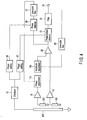
- a signal processing circuit of a sensing element 1 will now be described with reference to FIG. 4. Like reference numerals are used to designate the same portions as those of the foregoing embodiment, and a detailed description of those portions is omitted.
- This signal processing circuit is obtained by adding a function block to the aforementioned signal processing circuit.
- An amplifier 16 of a second coil 200 is connected to one input terminal of a differential amplifier 20 through a phase adjustment circuit 17a and an amplitude adjustment circuit 18a.
- the phase adjustment circuit 17a serves to adjust the phase of an input signal with use of a voltage signal as a control signal. It includes a photocoupler-based variable resistor, capacitor, operational amplifier, etc.
- the amplitude adjustment circuit 18a serves to change the amplification degree of an amplifier with use of a voltage signal as a control input, thereby adjusting the amplitude of an input signal. It includes a photocoupler-based variable resistor, fixed resistor, operational amplifier, etc.
- a low-pass filter 28 that is connected between the amplitude adjustment circuit 18a and a circuit output 24 outputs a very low frequency, such as a temperature drift.
- Another phase setting circuit 25 that is connected to an oscillator circuit 15 in parallel with a phase setting circuit 22 has its phase shifted at 90 degrees to the set phase value of the circuit 22.
- the phase setting circuit 25 is connected to the output side of the differential amplifier 20 through a phase detecting circuit 26.
- the detecting circuit 26 detects a signal of minimum sensitivity to the magnetic material from the output signal of the differential amplifier 20.
- the phase detecting circuit 26 is connected to the phase adjustment circuit 17a through a low-pass filter 27.
- the filter 27 like the low-pass filter 28, outputs a very low frequency.
- a phase detection signal with a phase shifted at 90 degrees to a phase detection signal with maximum sensitivity to the magnetic material is fed back to the phase adjustment circuit 17a and the amplitude adjustment circuit 18a, whereby the output of the differential amplifier 20 is reduced to zero for lower frequencies.
- compensation is made to a very low variation of the circuit output 24 caused by a temperature change or the like.
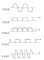
- the output of the phase detecting circuit 26 has the waveform shown in FIG. 5E, compared with the output waveform of the differential amplifier 20 shown in FIG. 5A, and an output V901 of the low-pass filter 27 is 0V.
- the output signal of the filter circuit 23 is fed back through the low-pass filter 28 to the amplitude adjustment circuit 18a at a low response speed. In consequence, the output of the differential amplifier 20 is reduced to zero.
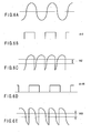
- the output of the phase-sensitive detecting circuit 21 has the waveform shown in FIG. 6C, and the filter circuit 23 has a DC voltage of V02 ( ⁇ V01) as its output.
- the output of the phase detecting circuit 26 has the waveform shown in FIG. 6E, compared with the output waveform of the differential amplifier 20 shown in FIG. 6A, and the output of the low-pass filter 27 is a DC voltage V902.
- the differential amplifier 20 can be operated with a high amplification factor without having its output saturated.
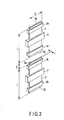
- the magnetic material detecting apparatus comprises a plurality of, e.g., seven, sensing elements 1 similar to the one shown in FIG. 1, which are arranged side by side.
- Each sensing element 1 includes a pair of cores 2 and 3.
- the sensing elements 1 are arranged in the width direction of a sheet 10 so that lines that connect first end portions 2a and 3a of their respective cores 2 and 3 extend parallel to one another.
- Each sensing element 1 is constructed in the same manner as the one according to the foregoing embodiment. Therefore, like reference numerals are used to designate like portions of the sensing elements, and a repeated description of those portions is omitted.
- a magnetic cover 8 is located so as to surround coils 5a and 6 that are wound on the seven cores 2.
- a magnetic cover 9 is located so as to surround coils 5b and 7 that are wound on the seven cores 2.
- Supports 11, 12, 13 and 14 for supporting the cores are arranged between the cores 2 and 3 and the magnetic covers 8 and 9. These supports are formed of a nonmagnetic material.
- the supports 11 to 14 each have a plurality of protrusions, which support the cores 2 and 3 by holding them from both sides.
- the protrusions of the supports 11 to 14 and the cores 2 and 3 may be fixed with a resin or the like that are filled into spaces between them.
- spaces between the adjacent sensing elements 1, especially a space p between each two adjacent cores 2 and a space p between each two adjacent cores 3, should be set to be equal to or wider than a gap G between the first end portions 2a and 3a of the cores 2 and 3, in order to reduce interference between the adjacent sensing elements 1.
- the magnetic material detecting apparatus comprises a shire conveyor mechanism 40, which conveys the sheet 10 through the gap G between the cores 2 and 3.
- the conveyor mechanism 40 has conveyor belts 42, conveyor pulleys 44, a drive unit (not shown) for driving the pulleys, etc.
- the conveyor belts 42 are so as to nip the transversely opposite end portions of the sheet 10 from both sides.
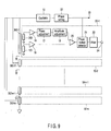
- the magnetic material detecting apparatus has n number of third coils 300-1, 300-2, ..., 300-n-1 and 300-n, which are formed by series-connecting the coils 6 and 7 that are wound on n pairs of cores. These third coils are connected in parallel with one another.
- a signal processing circuit of the detecting apparatus energizes the parallel-connected third coils 300-1, 300-2, ..., 300-n-1 and 300-n.
- the signal processing circuit is provided with n number of circuit elements 50-1, 50-2, ..., 50-n-1 and 50-n that are arranged corresponding to the n pairs of cores. Each circuit element is constructed in the same manner as a circuit element 50 of the signal processing circuit of FIG. 3, which is represented by a full enclosure line.
- the signal processing circuit comprises an oscillator circuit 15 that generates a signal for energizing the third coils 300.
- the third coils 300-1, 300-2, ..., 300-n-1 and 300-n are connected in parallel with the oscillator circuit 15.
- the circuit 15 is connected to a phase setting circuit 22, which serves as a second adjusting unit.
- An output 55 of the phase setting circuit 22 is connected to respective phase-sensitive detecting circuits 21 of the circuit elements 50-1, 50-2, ..., 50-n-1 and 50-n. With this arrangement, a detection signal can be obtained for each pair of cores.
- a magnetic material can be detected substantially covering the whole surface of the sheet 10 with respect to its width direction (perpendicular to the movement direction E), and the site of detection can be specified.
- a plurality of pairs of cores are arranged side by side, and the third coils are connected in parallel with one another and AC-energized, so that magnetic fields that are generated by the cores are in the same phase. If a plurality of sensing elements 1 are located close to one another, therefore, the adjacent cores interfere little with one another.
- detection signals that are induced in first and second coils 100 and 200 of the cores are also influenced little by the interference between the adjacent cores, so that the magnetic material detection can be performed with high accuracy.
- the magnetic material detecting apparatus can be reduced in overall size. Since the third coils are connected in parallel with each other, moreover, drive voltage for the third coils can be lowered provided that the current capacity is fixed.
- third coils are connected to the oscillator circuit 15 in parallel relation to one another according to the second embodiment, this invention is not limited to this arrangement.
- n number of third coils 300-1, 300-2, ..., 300-n-1 and 300-n are connected in series with one another and energized by signals from an oscillator circuit 15.
- the influence of interference between adjacent cores is so small that magnetic material detection can be performed with high accuracy.
- the magnetic material detecting apparatus can be reduced in overall size.
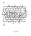
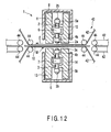
- the magnetic material detecting apparatus of this invention As shown in FIGS. 11 and 12, a plurality of sensing elements 1 are formed of a common core. More specifically, the detecting apparatus comprises two cores 62 and 63 in the form of an elongated rectangular plate each. Each core has a length substantially equal to the width of a sheet 10 as a medium to be detected. The two cores 62 and 63 are arranged so that their respective long sides extend parallel to the surface of the sheet 10 and are opposed to each other with a transfer path for the sheet between them.
- a plurality of first protrusions are formed integrally on that long side portion of the core 62 which is situated on the transfer path side and constitute first end portions 2a of the core, individually.
- the first end portions 2a are arranged at given spaces in the longitudinal direction of the core 62.
- a plurality of second protrusions are formed integrally on the opposite long side portion of the core 62 and constitute second end portions 2b, individually.
- the second end portions 2b are arranged at given spaces in the longitudinal direction of the core 62 and aligned with the first end portions 2a, individually.
- a plurality of protrusions are formed integrally on that long side portion of the core 63 which is situated on the transfer path side and constitute first end portions 3a, individually.
- the first end portions 3a are arranged at given spaces in the longitudinal direction of the core 63. Further, the first end portions 3a face their corresponding first end portions 2a of the core 62 with a gap G between them.
- a plurality of protrusions are formed integrally on the opposite long side portion of the core 63 and constitute second end portions 3b, individually.
- the second end portions 3b are arranged at given spaces in the longitudinal direction of the core 63 and aligned with the first end portions 3a, individually.
- Coils 4a are wound individually on the first end portions 2a of the core 62, and coils 5a on the second end portions 2b.
- a common coil 6 is wound on an intermediate portion of the core 62 and situated between the coils 4a and 5a.
- Coils 4b are wound individually on the first end portions 3a of the core 63, and coils 5b on the second end portions 3b.
- a common coil 7 is wound on an intermediate portion of the core 63 and situated between the coils 4b and 5b.
- a space p between each two adjacent first end portions 2a and a space p between each two adjacent first end portions 3a should be set to be equal to or wider than the gap G between the first end portions 2a and 3a, in order to reduce interference between the adjacent sensing elements 1.
- a magnetic cover 8 is located so as to surround the coils 5a and 6.
- a magnetic cover 9 is located so as to surround the coils 5b and 7.
- Supports 11, 12, 13 and 14 for supporting the cores are arranged between the cores 62 and 63 and the magnetic covers 8 and 9. These supports are formed of a nonmagnetic material.
- the supports 11 to 14 each have a plurality of protrusions, which support the cores 62 and 63 by holding them from both sides.
- the protrusions of the supports 11 to 14 and the cores 62 and 63 may be fixed with a resin or the like that are filled into spaces between them.
- Each sensing element is constructed in the same manner as the ones according to the foregoing embodiments. Therefore, like reference numerals are used to designate like portions of the sensing elements, and a repeated description of those portions is omitted.
- a signal processing circuit of the magnetic material detecting apparatus AC-energizes a common third coil 300 that is formed by series-connecting the two coils 6 and 7.
- the signal processing circuit is provided with n number of circuit elements 50-1, 50-2, ..., 50-n-1 and 50-n that are arranged corresponding to the sensing elements 1.
- Each circuit element is constructed in the same manner as the circuit element 50 of the enclosed signal processing circuit of FIG. 3.
- the signal processing circuit comprises an oscillator circuit 15 that generates a signal for energizing the third coil 300.
- the oscillator circuit 15 is connected to the third coil 300 and also to a phase setting circuit 22.
- An output 55 of the phase setting circuit 22 is connected to respective phase-sensitive detecting circuits 21 of the circuit elements 50-1, 50-2, ..., 50-n-1 and 50-n. With this arrangement, a detection signal can be obtained for each sensing element 1.
- the sensing elements are formed using the common cores 62 and 63 and the common coils 6 and 7, so that the detecting apparatus can be assembled with ease, and the gap G between the first end portions 2a and 3a of the cores can be adjusted at a time for the plurality of sensing elements.
- the present invention is not limited directly to the embodiments described above, and its components may be embodied in modified forms without departing from the scope or spirit of the invention. Further, various inventions may be made by suitably combining a plurality of components described in connection with the foregoing embodiments. For example, some of the components according to the foregoing embodiments may be omitted. Furthermore, the components according to the different embodiments may be combined as required.
- each of the cores that constitute each sensing element is not limited to the shape of a plate, and may be formed having any other shape, such as the shape of a rod.
- the medium to be detected is not limited to a sheet and may alternatively be a Belt-shaped film or any other medium that is coated with or contains a magnetic material.
Landscapes
- Engineering & Computer Science (AREA)
- Physics & Mathematics (AREA)
- Life Sciences & Earth Sciences (AREA)
- Remote Sensing (AREA)
- General Physics & Mathematics (AREA)
- Environmental & Geological Engineering (AREA)
- Electromagnetism (AREA)
- Theoretical Computer Science (AREA)
- Artificial Intelligence (AREA)
- Computer Vision & Pattern Recognition (AREA)
- Geology (AREA)
- General Life Sciences & Earth Sciences (AREA)
- Geophysics (AREA)
- Investigating Or Analyzing Materials By The Use Of Magnetic Means (AREA)
- Geophysics And Detection Of Objects (AREA)
- Measuring Magnetic Variables (AREA)
- Inspection Of Paper Currency And Valuable Securities (AREA)
Abstract
Description
Claims (13)
- A magnetic material detecting apparatus for detecting a magnetic material contained in a medium to be detected, characterized by comprising:a pair of cores (2, 3), each of which has a first end portion (2a, 3a), a second end portion (2b, 3b) opposite to the first end portion, and an intermediate portion between the first and second end portions, the respective first end portions of the cores being opposed to each other across a gap (G) with a transfer path (M) for the passage of the medium (10) to be detected therebetween;a first coil (100) including coils (4a, 4b) which are wound individually on the respective first end portions of the cores and connected in series with each other;a second coil (200) including coils (5a, 5b) which are wound individually on the respective second end portions of the cores and connected in series with each other;a third coil (300) including coils (6, 7) which are wound individually on the respective intermediate portions of the cores and connected in series with each other; anda signal processing circuit which AC-energizes the third coil (300) to process a detection signal from the first coil (100) and a detection signal from the second coil (200).
- A magnetic material detecting apparatus according to claim 1, characterized by further comprising magnetic covers (8, 9) of a magnetic material which individually surround the respective second end portions (5a, 5b) of the paired cores (2, 3).
- A magnetic material detecting apparatus according to claim 1, characterized in that each of the cores (2, 3) is formed by laminating amorphous foils together.
- A magnetic material detecting apparatus according to claim 2, characterized in that a gap between the cores (2, 3) and the magnetic covers (8, 9) is wider than a gap between the first and second end portions (2a, 3a, 2b, 3b) of the cores.
- A magnetic material detecting apparatus according to claim 2, characterized in that each of the magnetic covers (2, 3) has an open end which opens on the transfer path side, and a gap (Q) between the first end portion (2a, 3a) of each core and the open end of the magnetic cover (8, 9) is wider than the gap (G) between the respective first end portions of the paired cores.
- A magnetic material detecting apparatus according to claim 1, characterized in that the signal processing circuit comprises a first adjustment circuit (17, 18) which adjusts the phase and amplitude of the detection signal from the first or second coil (100 or 200), a unit (20) which obtains a difference signal in accordance with the phase and amplitude of the detection signal from the second or first coil, a second adjustment circuit (22) which adjusts the phase of an AC signal which energizes the third coil (300), and a smoothing unit (21) which detects and smoothes the phase of the difference signal with use of an output of the second adjustment circuit as a reference waveform.
- A magnetic material detecting apparatus according to claim 6, characterized in that the signal processing circuit comprises a first phase setting circuit adjusted to a phase which maximizes a magnetic material detection signal from the difference signal, a second phase setting circuit adjusted to a phase which is shifted at 90 degrees to the phase which maximizes the magnetic material detection signal, a first adjusting unit which adjusts the amplitude of the first or second detection signal in response to an output signal from the first phase setting circuit, and a second adjusting unit which adjusts the phase of the first or second detection signal in response to an output signal from the second phase setting circuit.
- A magnetic material detecting apparatus for detecting a magnetic material contained in a medium to be detected, characterized by comprising:a plurality of sensing elements (1) arranged side by side; andmagnetic covers (8, 9) of a magnetic material which individually surround at least parts of the sensing elements exclusive of a transfer path (M) along which the medium (10) to be detected is conveyed;each of the sensing elements (1) including:a pair of cores (2, 3), each of which has a first end portion (2a, 3a), a second end portion (2b, 3b) opposite to the first end portion, and an intermediate portion between the first and second end portions, the respective first end portions of the cores being opposed to each other across a gap (G) with the transfer path for the passage of the medium to be detected therebetween,a first coil (100) including coils (4a, 4b) which are wound individually on the respective first end portions of the cores and connected in series with each other,a second coil (200) including coils (5a, 5b) which are wound individually on the respective second end portions of the cores and connected in series with each other,a third coil (300) including coils (6, 7) which are wound individually on the respective intermediate portions of the cores and connected in series with each other, anda signal processing circuit which AC-energizes the third coil to process a detection signal from the first coil and a detection signal from the second coil,the sensing elements being arranged side by side so that lines connecting the respective first end portions of the paired cores of the sensing elements are parallel to one another.
- A magnetic material detecting apparatus according to claim 8, characterized in that the respective third coils (300) of the sensing elements are connected in series with one another.
- A magnetic material detecting apparatus according to claim 8, characterized in that the respective third coils (300) of the sensing elements are connected in parallel with one another.
- A magnetic material detecting apparatus according to claim 8, characterized in that the signal processing circuit comprises a plurality of circuit elements (50, 50-1, ..., 50-n) provided individually for the first and second coils (100, 200) of the sensing elements (1), each of the circuit elements including a first adjustment circuit (17, 18) which adjusts the phase and amplitude of the detection signal from the first or second coil, a unit which obtains a difference signal in accordance with the phase and amplitude of the detection signal from the second or first coil, a second adjustment circuit (22) which adjusts the phase of an AC signal which energizes the third coil, and a smoothing unit (21) which detects and smoothes the phase of the difference signal with use of an output of the second adjustment circuit as a reference waveform.
- A magnetic material detecting apparatus for detecting a magnetic material contained in a medium to be detected, characterized by comprising:a pair of platelike cores (62, 63) each having a pair of long side portions opposite to each other, an intermediate portion situated between the long side portions, a plurality of first protrusions (2a, 3a) arranged spaced from one another on one of the long side portions, and a plurality of second protrusions (2b, 3b) arranged spaced from one another on the other long side portion, the paired cores being arranged so that the first protrusions of one of the cores and the first protrusions of the other core are opposed to one another across a given gap (G) with a transfer path (M) for the passage of the medium (10) to be detected therebetween;a plurality of first coils (100) each including a plurality of coils (4a, 4b) which are wound individually on the opposite first protrusions of each set on the paired cores and connected in series for each set;a plurality of second coils (200) each including a plurality of coils (5a, 5b) which are wound individually on the second protrusions of each set on the paired cores and connected in series for each set;a third coil (300) including two coils (6, 7) which are wound individually on the respective intermediate portions of the paired cores;a pair of magnetic covers (8, 9) of a magnetic material which individually surround the respective second-protrusion-side long side portions of the cores; anda signal processing circuit which AC-energizes the third coil to process a plurality of detection signals from the first coils and a plurality of detection signals from the second coils.
- A magnetic material detecting apparatus, according to claim 12, characterized in that the signal processing circuit comprises a plurality of circuit elements (1) provided individually for the sets of first and second coils (100, 200), each of the circuit elements including a first adjustment circuit (17, 18) which adjusts the phase and amplitude of the detection signal from the first or second coil, a unit which obtains a difference signal in accordance with the phase and amplitude of the detection signal from the second or first coil, a second adjustment circuit (22) which adjusts the phase of an AC signal which energizes the third coil, and a smoothing unit (21) which detects and smoothes the phase of the difference signal with use of an output of the second adjustment circuit as a reference waveform.
Applications Claiming Priority (2)
| Application Number | Priority Date | Filing Date | Title |
|---|---|---|---|
| JP2004054911 | 2004-02-27 | ||
| JP2004054911A JP4227038B2 (en) | 2004-02-27 | 2004-02-27 | Magnetic detection device |
Publications (3)
| Publication Number | Publication Date |
|---|---|
| EP1571463A2 true EP1571463A2 (en) | 2005-09-07 |
| EP1571463A3 EP1571463A3 (en) | 2007-05-30 |
| EP1571463B1 EP1571463B1 (en) | 2010-04-28 |
Family
ID=34747571
Family Applications (1)
| Application Number | Title | Priority Date | Filing Date |
|---|---|---|---|
| EP05002723A Expired - Lifetime EP1571463B1 (en) | 2004-02-27 | 2005-02-09 | Magnetic material detecting apparatus |
Country Status (6)
| Country | Link |
|---|---|
| US (1) | US7012424B2 (en) |
| EP (1) | EP1571463B1 (en) |
| JP (1) | JP4227038B2 (en) |
| CN (1) | CN100516864C (en) |
| AT (1) | ATE466301T1 (en) |
| DE (1) | DE602005020870D1 (en) |
Cited By (1)
| Publication number | Priority date | Publication date | Assignee | Title |
|---|---|---|---|---|
| WO2014084035A1 (en) * | 2012-11-28 | 2014-06-05 | 日本電産サンキョー株式会社 | Magnetic sensor device |
Families Citing this family (17)
| Publication number | Priority date | Publication date | Assignee | Title |
|---|---|---|---|---|
| JP2005181173A (en) * | 2003-12-22 | 2005-07-07 | Toshiba Corp | Magnetic quantity detector |
| JP4483497B2 (en) * | 2004-09-16 | 2010-06-16 | 富士ゼロックス株式会社 | Magnetic detection device |
| JP4675704B2 (en) | 2005-07-13 | 2011-04-27 | 株式会社東芝 | Magnetic detection device |
| CN102213753A (en) * | 2011-01-14 | 2011-10-12 | 西北核技术研究所 | Test method and device of magnetization characteristic of magnetic core under fast pulse voltage |
| JP5603259B2 (en) * | 2011-01-14 | 2014-10-08 | 日立オムロンターミナルソリューションズ株式会社 | Paper sheet identification device |
| US9488747B2 (en) * | 2012-03-23 | 2016-11-08 | Seesoon, Inc. | Gradient antenna coils and arrays for use in locating systems |
| DE102012205283A1 (en) * | 2012-03-30 | 2013-10-02 | Bayerische Motoren Werke Aktiengesellschaft | Device for inductive power transmission |
| DE102013205891A1 (en) * | 2013-04-03 | 2014-10-09 | Giesecke & Devrient Gmbh | Examination of a security element provided with magnetic materials |
| JP6226629B2 (en) | 2013-08-09 | 2017-11-08 | 株式会社東芝 | Magnetic detection device and paper sheet processing device |
| CN103544764B (en) * | 2013-09-12 | 2016-11-16 | 无锡乐尔科技有限公司 | A kind of sensor for identifying magnetic medium |
| JP6590526B2 (en) * | 2015-05-22 | 2019-10-16 | アンリツインフィビス株式会社 | Metal detector |
| JP6590525B2 (en) * | 2015-05-22 | 2019-10-16 | アンリツインフィビス株式会社 | Metal detector |
| US9577185B1 (en) * | 2016-04-28 | 2017-02-21 | Texas Instruments Incorporated | Fluxgate device with low fluxgate noise |
| CN113359092B (en) * | 2021-06-05 | 2022-12-13 | 自然资源部第一海洋研究所 | Miniaturized broadband magnetic receiving module of high-frequency radar and array element and method thereof |
| JP7532315B2 (en) * | 2021-06-28 | 2024-08-13 | 株式会社荏原製作所 | EDDY CURRENT SENSOR DETECTION SIGNAL PROCESSING APPARATUS AND DETECTION SIGNAL PROCESSING METHOD |
| US12111187B2 (en) * | 2021-09-17 | 2024-10-08 | Sensata Technologies, Inc. | Inductive position sensor with coil configuration |
| CN120143027B (en) * | 2025-05-14 | 2025-08-22 | 中国计量科学研究院 | A non-destructive measurement device and method for determining the orientation direction of a permanent magnet |
Family Cites Families (6)
| Publication number | Priority date | Publication date | Assignee | Title |
|---|---|---|---|---|
| KR100427628B1 (en) * | 1995-11-10 | 2004-07-12 | 신코스모스덴끼 가부시끼가이샤 | Magnetic concentration measurement method and device |
| JPH09236642A (en) | 1996-03-04 | 1997-09-09 | Toshiba Corp | Magnetic substance detection device |
| JP3971091B2 (en) * | 2000-07-21 | 2007-09-05 | 株式会社東芝 | Magnetic detection device |
| JP2002074446A (en) * | 2000-09-04 | 2002-03-15 | Toshiba Corp | Magnetic body identification device |
| JP2002230617A (en) * | 2001-01-30 | 2002-08-16 | Toshiba Corp | Magnetic detection device for paper sheets |
| JP2002350405A (en) * | 2001-05-28 | 2002-12-04 | Toshiba Corp | Magnetic detection device for paper sheets |
-
2004
- 2004-02-27 JP JP2004054911A patent/JP4227038B2/en not_active Expired - Fee Related
-
2005
- 2005-02-09 DE DE602005020870T patent/DE602005020870D1/en not_active Expired - Lifetime
- 2005-02-09 EP EP05002723A patent/EP1571463B1/en not_active Expired - Lifetime
- 2005-02-09 AT AT05002723T patent/ATE466301T1/en active
- 2005-02-22 US US11/062,452 patent/US7012424B2/en not_active Expired - Lifetime
- 2005-02-25 CN CNB2005100524313A patent/CN100516864C/en not_active Expired - Fee Related
Cited By (1)
| Publication number | Priority date | Publication date | Assignee | Title |
|---|---|---|---|---|
| WO2014084035A1 (en) * | 2012-11-28 | 2014-06-05 | 日本電産サンキョー株式会社 | Magnetic sensor device |
Also Published As
| Publication number | Publication date |
|---|---|
| US20050189939A1 (en) | 2005-09-01 |
| CN1661365A (en) | 2005-08-31 |
| US7012424B2 (en) | 2006-03-14 |
| ATE466301T1 (en) | 2010-05-15 |
| DE602005020870D1 (en) | 2010-06-10 |
| EP1571463B1 (en) | 2010-04-28 |
| JP2005241594A (en) | 2005-09-08 |
| CN100516864C (en) | 2009-07-22 |
| EP1571463A3 (en) | 2007-05-30 |
| JP4227038B2 (en) | 2009-02-18 |
Similar Documents
| Publication | Publication Date | Title |
|---|---|---|
| EP1571463B1 (en) | Magnetic material detecting apparatus | |
| USRE42159E1 (en) | Circuit for compensation for time variation of temperature in an inductive sensor | |
| CN111505363A (en) | A closed loop current transformer | |
| KR101921440B1 (en) | Magnetic sensor device | |
| JP2009186433A (en) | Eddy current sample measurement method, eddy current sensor, and eddy current sample measurement system | |
| JP7119633B2 (en) | magnetic sensor | |
| JP2008145379A (en) | Magnetic sensor | |
| EP1744182B1 (en) | Magnetic material detecting apparatus | |
| JP2005030872A (en) | Magnetic quantity detector | |
| JP4267271B2 (en) | Magnetic detection device | |
| JP7119695B2 (en) | magnetic sensor | |
| JP2020041869A (en) | Magnetic sensor | |
| JP3971091B2 (en) | Magnetic detection device | |
| JP4104923B2 (en) | Magnetic body detection device | |
| EP1548658A1 (en) | Magnetic material amount detecting apparatus | |
| JP2002350405A (en) | Magnetic detection device for paper sheets | |
| JP6263664B1 (en) | Magnetic ink detection device | |
| JP2021028596A (en) | Zero-flux type magnetic sensor | |
| JP2008145302A (en) | Magnetic sensor | |
| US20240387084A1 (en) | Magnetic Core for Current Sensors | |
| JPH09236642A (en) | Magnetic substance detection device | |
| JPH07280587A (en) | Position detector using differential transformer | |
| JPH0743105A (en) | Position detector | |
| JP2020024772A (en) | Differential type magnetic head |
Legal Events
| Date | Code | Title | Description |
|---|---|---|---|
| PUAI | Public reference made under article 153(3) epc to a published international application that has entered the european phase |
Free format text: ORIGINAL CODE: 0009012 |
|
| 17P | Request for examination filed |
Effective date: 20050209 |
|
| AK | Designated contracting states |
Kind code of ref document: A2 Designated state(s): AT BE BG CH CY CZ DE DK EE ES FI FR GB GR HU IE IS IT LI LT LU MC NL PL PT RO SE SI SK TR |
|
| AX | Request for extension of the european patent |
Extension state: AL BA HR LV MK YU |
|
| PUAL | Search report despatched |
Free format text: ORIGINAL CODE: 0009013 |
|
| AK | Designated contracting states |
Kind code of ref document: A3 Designated state(s): AT BE BG CH CY CZ DE DK EE ES FI FR GB GR HU IE IS IT LI LT LU MC NL PL PT RO SE SI SK TR |
|
| AX | Request for extension of the european patent |
Extension state: AL BA HR LV MK YU |
|
| RIC1 | Information provided on ipc code assigned before grant |
Ipc: G01V 3/10 20060101AFI20050714BHEP Ipc: G07D 7/04 20060101ALI20070420BHEP |
|
| AKX | Designation fees paid |
Designated state(s): AT DE FR IT |
|
| GRAP | Despatch of communication of intention to grant a patent |
Free format text: ORIGINAL CODE: EPIDOSNIGR1 |
|
| GRAS | Grant fee paid |
Free format text: ORIGINAL CODE: EPIDOSNIGR3 |
|
| GRAA | (expected) grant |
Free format text: ORIGINAL CODE: 0009210 |
|
| AK | Designated contracting states |
Kind code of ref document: B1 Designated state(s): AT DE FR IT |
|
| REF | Corresponds to: |
Ref document number: 602005020870 Country of ref document: DE Date of ref document: 20100610 Kind code of ref document: P |
|
| PLBE | No opposition filed within time limit |
Free format text: ORIGINAL CODE: 0009261 |
|
| STAA | Information on the status of an ep patent application or granted ep patent |
Free format text: STATUS: NO OPPOSITION FILED WITHIN TIME LIMIT |
|
| PG25 | Lapsed in a contracting state [announced via postgrant information from national office to epo] |
Ref country code: IT Free format text: LAPSE BECAUSE OF FAILURE TO SUBMIT A TRANSLATION OF THE DESCRIPTION OR TO PAY THE FEE WITHIN THE PRESCRIBED TIME-LIMIT Effective date: 20100428 |
|
| 26N | No opposition filed |
Effective date: 20110131 |
|
| REG | Reference to a national code |
Ref country code: FR Ref legal event code: PLFP Year of fee payment: 11 |
|
| PGFP | Annual fee paid to national office [announced via postgrant information from national office to epo] |
Ref country code: DE Payment date: 20150203 Year of fee payment: 11 |
|
| PGFP | Annual fee paid to national office [announced via postgrant information from national office to epo] |
Ref country code: AT Payment date: 20150126 Year of fee payment: 11 Ref country code: FR Payment date: 20150210 Year of fee payment: 11 |
|
| REG | Reference to a national code |
Ref country code: DE Ref legal event code: R119 Ref document number: 602005020870 Country of ref document: DE |
|
| REG | Reference to a national code |
Ref country code: AT Ref legal event code: MM01 Ref document number: 466301 Country of ref document: AT Kind code of ref document: T Effective date: 20160209 |
|
| REG | Reference to a national code |
Ref country code: FR Ref legal event code: ST Effective date: 20161028 |
|
| PG25 | Lapsed in a contracting state [announced via postgrant information from national office to epo] |
Ref country code: AT Free format text: LAPSE BECAUSE OF NON-PAYMENT OF DUE FEES Effective date: 20160209 |
|
| PG25 | Lapsed in a contracting state [announced via postgrant information from national office to epo] |
Ref country code: FR Free format text: LAPSE BECAUSE OF NON-PAYMENT OF DUE FEES Effective date: 20160229 Ref country code: DE Free format text: LAPSE BECAUSE OF NON-PAYMENT OF DUE FEES Effective date: 20160901 |