EP1566935B1 - Vorrichtung und Verfahren zur Unterdrückung von Impulsinterferenzen in einem Signal - Google Patents
Vorrichtung und Verfahren zur Unterdrückung von Impulsinterferenzen in einem Signal Download PDFInfo
- Publication number
- EP1566935B1 EP1566935B1 EP05101201A EP05101201A EP1566935B1 EP 1566935 B1 EP1566935 B1 EP 1566935B1 EP 05101201 A EP05101201 A EP 05101201A EP 05101201 A EP05101201 A EP 05101201A EP 1566935 B1 EP1566935 B1 EP 1566935B1
- Authority
- EP
- European Patent Office
- Prior art keywords
- signal
- digital values
- coefficient
- successive digital
- time period
- Prior art date
- Legal status (The legal status is an assumption and is not a legal conclusion. Google has not performed a legal analysis and makes no representation as to the accuracy of the status listed.)
- Expired - Lifetime
Links
Images

Classifications
-
- H—ELECTRICITY
- H04—ELECTRIC COMMUNICATION TECHNIQUE
- H04L—TRANSMISSION OF DIGITAL INFORMATION, e.g. TELEGRAPHIC COMMUNICATION
- H04L27/00—Modulated-carrier systems
- H04L27/26—Systems using multi-frequency codes
- H04L27/2601—Multicarrier modulation systems
- H04L27/2647—Arrangements specific to the receiver only
Definitions
- the present invention relates to a device and method for suppressing impulse interference contained in a signal.
- the present invention relates to a device and a method for suppressing impulse interference for a Coded Orthogonal Frequency Division Multiplex (COFDM) demodulator.
- COFDM Coded Orthogonal Frequency Division Multiplex
- data packets to be transmitted are put in the form of N complex coefficients associated with N respective frequencies (or carriers).
- the number N of the frequencies is equal for example to 1705 for the so-called “2K” mode and 6817 for the so-called “8K” mode, in digital terrestrial television transmission. All these N coefficients are processed by inverse fast Fourier transform (IFFT), which produces a "symbol” consisting of a sum of modulated carriers, each carrier having an amplitude and a phase determined by the associated complex coefficient. The symbol thus generated is emitted.
- IFFT inverse fast Fourier transform
- the useful life is of the order of 224 ⁇ s in 2K mode and 896 ⁇ s in 8K mode, for a bandwidth of 8 MHz.
- a receiver On reception, a receiver makes the symbol undergo inverse processing, that is to say mainly a fast Fourier transform (FFT) to reconstruct the complex initial coefficients.
- FFT fast Fourier transform
- pilots Some carriers of the modulated signal, called pilots, are used during the demodulation to determine an estimate of the frequency response of the transmission channel used and to realize the fast Fourier transform of the modulated signal.
- the signal received by the COFDM demodulator corresponds to the transmitted modulated signal modified by disturbances of various origins. It is therefore necessary to correct the received signal to find the transmitted symbols.
- transmission noise generally corresponds to a low-energy disturbance which is permanently present and which is characteristic of the transmission channel used by the signal between the receiver and the transmitter.
- impulse interference corresponds to disturbances that are very short in duration but have a high energy. These are disturbances that are neither reproducible nor predictable, that are not present all the time, and that can occur in isolation or grouped at any given moment with amplitude, duration, and momentum. departure not predictable.
- Impulse interference is, for example, due to electrical equipment located near the components of the demodulator.
- the transmission noise correction generally uses the temporal stability properties of such a disturbance.
- the correction of the impulse interferences generally involves a method of individually detecting each impulse interference and correcting the modulated signal received when impulse interference is detected.
- An exemplary method of detecting and correcting classical pulse interference is the zero-substitution threshold detection method.
- Such a method is, for example, implemented on the reference demodulator STV0360, marketed by the Applicant.
- the aim is to detect the presence of impulse interference by comparing, at a determined comparison threshold, the amplitude of a digital modulated signal obtained by analog-to-digital conversion of the analog modulated signal received by the demodulator, generally after a change of frequency to an intermediate frequency range. All numerical values of the digital modulated signal higher than the determined threshold are replaced by a predetermined value, for example the average value of the signal.
- the main difficulty of threshold detection is the choice of the comparison threshold. Indeed, if the threshold is too high, only very high energy impulse interference is detected and impulse interference of a lower energy level may not be detected. Conversely, if the detection threshold is too low, part of the digital modulated signal undisturbed by impulse interference can be suppressed.
- the present invention provides a device and a method for suppressing impulse interference disturbing a signal, in particular a signal received by a COFDM demodulator, allowing the suppression of high energy impulse interference, but also moderate energy impulse interference, while limiting the risk of inaccurate detection of impulse interference.
- the present invention provides a device for suppressing impulse interference contained in a signal according to claim 1.
- the present invention also provides a method of suppressing impulse interference contained in a signal according to claim 7.
- the present invention will now be described for a COFDM demodulator. It is clear that the present invention finds application for any type of signal processing system disturbed by impulse interference that is to be corrected.
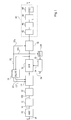
- the figure 1 represents, in more detail, an exemplary COFDM demodulator according to the invention.
- An input E of the demodulator receives an intermediate frequency IF signal enabling sampling, for example 36 MHz.
- the signal IF corresponds to the signal received after various changes or transpositions of frequency.
- the input E is coupled to an analog-to-digital converter (ADC) which digitizes the IF input signal.
- ADC analog-to-digital converter
- the analog-to-digital converter 10 provides an IS signal at a module 11 for suppressing impulse interference.
- the module 11 supplies an OS signal corresponding to the signed signal IS in which the impulse interferences are suppressed.
- the module 11 attacks a module 12 of frequency change.
- the module 12 provides a signal substantially in baseband, the spectrum of the signal at the output of the module 12 being centered on a frequency substantially equal to zero.
- the module 12 is coupled to a module 14 allowing on the one hand a fine adjustment of the center frequency of the signal spectrum and, on the other hand, to provide temporal samples at times appropriate to the subsequent processing.
- the spectrum of the signal is centered on a frequency equal to 0 and the number and the temporal position of the samples are adapted to the transformation by Fourier transform which takes place in the following module.
- the module 14 is controlled by links 15 and 15 'connecting the module 14 to a module 16 for processing the pilots.
- the output of the module 14 drives a Fast Fourier Transform (FFT) module 20 which provides the frequencies corresponding to a symbol.
- FFT Fast Fourier Transform
- the module 20 is controlled by a module 22 which provides, via a link 24, a signal for adjusting the analysis window of the Fourier transform.
- the output of the module 20 is coupled to the module 16 which carries out the extraction and the processing of the pilots.
- the module 16 provides on the links 15 and 15 'the signals intended to correct the central frequency of the spectrum and the sampling frequency of the signal.
- the output of the module 20 drives a module 30 in which the signal is corrected using an estimate of the frequency response of the channel.
- the estimation of the frequency response of the channel is carried out in module 16 using the drivers. This estimate is provided by the module 16 on a link 55, a branch 55a of which is coupled to the module 30.
- the signal notably comprises the carriers carrying the data.
- the estimation of the frequency response of the channel, provided by the module 16, supplies, via the link 55 and a branch 55b of the link 55, a module 26 of the inverse Fourier transform (IFFT), for determine the impulse response of the channel.
- the module 26 provides the impulse response of the channel to the module 22, to dynamically adjust the positioning of the FFT analysis window.
- the processing of the carriers carrying the data is provided in a circuit 40 for processing and supplying data.
- the circuit 40 has a conventional structure and may comprise, as shown in FIG. figure 4 , a symbol deinterleaving module 42, a "demapping" module 44, a bit deinterleaving module 46, and an error correction module 48 (FEC).
- the output of the module 48 constitutes the output S of the circuit 40 and the demodulator and supplies data corresponding to the data transmitted.
- the module 22 receives the output signal of the module 14 via a link 54, to roughly adjust the analysis window.
- the figure 2 schematically represents an exemplary embodiment of the impulse interference suppression module 11 according to the invention.
- the module 11 receives the signal IS at the output of the analog / digital converter 10, and supplies the output signal OS which drives the baseband signal transfer module 12.
- the module 11 comprises a memory 60 adapted to simultaneously store the last N successive digital values of the input signal IS received by the module 11, N being for example an even natural integer of the order of 32 to 64.
- the value of the signal IS of time t0 will be called the most recent digital value of the signal IS received by the module 11 and the values of the signal IS respectively of instants t1 to tN, the N successive digital values of the signal IS stored. in the memory 60, the digital value of the signal IS of instant tN being the oldest.
- the module 11 comprises a module 62 for determining a coefficient COEFF1 representative of the evolution of the input signal IS for the last N digital values of the received signal IS, hereinafter called the short-term evolution coefficient, which, by For example, simultaneously receives the digital value of the signal IS of time t0 and the digital value of the signal IS of instant tN stored in the memory 60 or which receives all the values stored in the memory 60.
- the module 11 comprises a module 64 of determination of a coefficient COEFF2 representative of the evolution of the signal received by the demodulator for a number of recently received digital values substantially greater than N, hereinafter referred to as the long-term evolution coefficient, which receives the digital value of the signal IS d moment t0.
- a comparator module 66 determines the presence or absence of impulse interference on the last N digital values of the signal IS received by comparing the short-term evolution coefficients COEFF1 and long-term COEFF2 with a determined comparison criterion.
- a correction module 68 receives the digital value of the signal IS of instant N / 2 stored in the memory 60 and the output of the comparator module 66 and corrects the digital value of the signal IS of time tN / 2 to supply the digital output signal OS if the comparator module 66 has detected the presence of impulse interference.
- the correction made by the correction module 68 consists in replacing the digital value of the input signal IS of time tN / 2, provided by the memory 60, by a mean value, or by a constant value. any, to the detection of impulse interference.
- an evolution coefficient adapted to the detection of impulse interference is the standard deviation.
- the calculation of the standard deviation requires the carrying out of multiplication operations which, when they are carried out by an integrated circuit, require a circuit occupying a large silicon surface. It may therefore be advantageous to use a coefficient corresponding to an approximation of the standard deviation and the calculation of which essentially uses additions that can be performed by a circuit occupying a reduced silicon area.
- the evolution coefficient used is the sum of the absolute values of numerical values, possibly corrected, of the digital signal IS. Such a coefficient provides information similar to that of the standard deviation, and will therefore be called pseudo standard deviation coefficient.
- the long-term pseudo standard deviation coefficient COEFF2 determined from a relatively large number of successive digital values of the input signal IS, tends towards the pseudo-standard deviation coefficient that would be obtained with an undisturbed input signal IS by impulse interference.
- the short-lived pseudo standard deviation coefficient COEFF1 determined for a smaller number N of successive digital values of the digital input signal IS, varies significantly when an impulse interference is present on the N successive numerical values used for the calculation. pseudo standard deviation short-term.
- the figure 3 represents a more detailed example of embodiment of module 11 of the figure 2 .
- the module 62 for determining the short-period pseudo-standard deviation coefficient comprises an absolute value module 70 which receives the successive digital values of the signal IS of instant tN stored in the memory 60 and which provides a signal I1 corresponding to the absolute values of the successive numerical values of the signal IS of instant tN.
- the absolute value module 70 drives a comparator-corrector module 72.
- the comparator-corrector module 72 compares the signal I1 with a threshold SEUIL1. If the signal I1 is below the threshold SEUIL1, the comparator-corrector 72 provides a signal OUT1 equal to the signal I1, unmodified.
- the comparator-corrector 72 provides a signal OUT1 equal to a weighting constant VAL1.
- the module 62 comprises an absolute value module 74 which supplies a signal 12 corresponding to the absolute values of the successive digital values of the signal IS of time t0 and which drives a comparator-corrector module 76, analogous to the module 72.
- the comparator module -corrector 74 compares the signal 12 to a threshold SEUIL2. If the signal 12 is below the threshold SEUIL2, the comparator-corrector 74 provides a signal OUT2 equal to the signal 12, unmodified.
- the comparator-corrector 74 provides a signal OUT2 equal to a weighting constant VAL2.
- the thresholds SEUIL1 and SEUIL2 are identical and the weighting constants VAL1 and VAL2 are identical and equal to a multiple of the threshold SEUIL1, for example, four times the threshold SEUIL1.
- the module 62 comprises an adder-subtractor 78 receiving the signals OUT1 and OUT2 and the output of a memory 80 in which is stored the last value supplied by the adder-subtractor 78.
- the adder-subtracter 78 performs the sum of the content of the memory 80 and the signal OUT2 to which it subtracts the signal OUT2.
- the adder-subtractor 78 supplies, at an input A of the comparator module 66, a signal COEFF1, corresponding to the pseudo short-term standard deviation coefficient, which is equal to the sum of N successive values of the signal OUT3.
- a signal COEFF1 corresponding to the pseudo short-term standard deviation coefficient, which is equal to the sum of N successive values of the signal OUT3.
- the use of the weighting constants VAL1, VAL2 makes it possible to accentuate the weight of the values of the signal 12 of high amplitude in the determination of the coefficient COEFF1.
- the module 64 for determining the long-term pseudo standard deviation coefficient comprises the absolute value module 74, in common with the module 62, which drives a comparator-corrector module 82 similar to the modules 72, 76.
- the comparator-corrector module 82 compares the signal 12 at a threshold THRESHOLD3. If the signal 12 is below the threshold SEUIL3, the comparator-corrector 82 provides a signal OUT3 equal to the signal 12, unmodified. If the signal 12 is greater than the threshold SEUIL3, the comparator-corrector 82 provides a signal OUT3 equal to a weighting constant VAL3.
- the weighting constant VAL3 is zero, which makes it possible to exclude the values of the signal 12 whose amplitude is very high in the determination of the long-term pseudo standard deviation coefficient.
- the module 64 comprises an adder 84 receiving the signal OUT3 and the output of a multiplexer 86.
- the multiplexer 86 receives at a first input the contents of a memory 88 in which the null value is stored and at a second input the content of the memory.
- a memory 90 in which the signal supplied by the adder 84 is stored.
- the adder 84 drives a module 92 dividing the signal supplied by the adder 84 by a scale factor Sc.
- the output of the module 92 attacks a flip-flop 94 controlled by a control signal COM.
- the flip-flop 94 supplies a COEFF2 signal, corresponding to the long-term pseudo standard deviation coefficient.
- the multiplexer 86 is controlled by the control signal COM. As will be described in more detail below, the control signal COM is substantially continuously zero. The multiplexer 86 then supplies the contents of the memory 90. The adder 84 thus adds to the signal OUT3 the contents of the memory 90, the sum being stored again in the memory 90. The sum of the digital values constituting the signal OUT3, divided by the scaling coefficient Sc, is therefore provided at the input of the flip-flop 94 which remains blocked. When the sum is done for N x Sc successive values of the signal OUT3, the control signal COM goes to 1 during an operating clock cycle of the module 11.
- the flip-flop 94 then becomes conducting and therefore provides the signal COEFF2 corresponding to the sum, divided by the scale factor Sc, N x Sc the last successive values of the signal OUT3. Since the control signal COM is at 1, the multiplexer 86 supplies the null value, and the adder 84 outputs the signal OUT3. The control signal COM returns to 0 at the next clock cycle, resulting in the calculation of the sum of the N x Sc values of the signal OUT3. The signal COEFF2, supplied by the module 64, is thus "refreshed" every N x Sc clock cycles.
- the module 64 comprises a memory 98 supplying, at each clock cycle, the value 1 to an adder 100 which also receives the output of a multiplexer 102 and providing an incrementation signal. COUNT.
- the multiplexer 102 receives at an input the contents of a memory 104 in which the null value is stored and at another input the contents of a memory 106 in which the incrementation signal COMPT is stored.
- the multiplexer 102 is controlled by the control signal COM. As long as the control signal COM is equal to 0, the multiplexer 102 supplies the adder 100 with the output of the memory 106. In this case, at each clock cycle, the incrementation signal COMPT increases by one unit .
- the adder 100 drives a comparator 107 which compares the incrementation signal COMPT with a threshold equal to the product of the integer N and the scale factor Sc.
- the scale factor Sc is equal to several hundred.
- the comparator 107 provides the command signal COM which is equal to the value 1 when the incrementation signal COMPT is greater than N ⁇ Sc, and equal to 0 when the incrementation signal COMPT is smaller than N ⁇ Sc.
- the control signal COM goes to 1
- the multiplexer 102 provides the zero value and the incrementation signal COMPT returns to 1.
- the control signal COM then returns to zero.
- the COM control signal therefore retains the value 1 for a single clock cycle.
- the signal COEFF2 corresponds to the sum, divided by the scale factor Sc, of N x Sc successive values of the signal OUT3, that is to say for a larger number of values, of the factor Sc, than the number of values used for the supply of the COEFF1 signal.
- the comparator module 66 comprises a module 108 receiving the signal COEFF2, supplied by the flip-flop 94, and which multiplies the signal COEFF2 by a corrective coefficient Corr.
- the corrective coefficient Corr is equal to 3.
- the comparator module 66 comprises a comparator 109 receiving at an input A the signal COEFF1 and at an input B the output of the module 108.
- the comparator 109 provides a signal equal to 1 if the signal received at the input A is greater than the signal received at the input B and provides a signal equal to 0 otherwise.
- the corrector module 68 comprises a multiplexer 110 controlled by the output of the comparator 109 and receiving at a first input the contents of a memory 112 in which a weighting constant is stored, generally a value less than unity, for example the value null, and at a second input the contents of a memory 114 in which is stored the value 1.
- the multiplexer 110 attacks a multiplier 112 which provides the output signal OS.
- the multiplexer 110 provides the weighting constant stored in the memory 112
- the signal OS is equal to the value of the input signal IS of time tN / 2 stored in the memory 60 multiplied by the weighting constant stored in the memory 112.
- the multiplexer 110 When the signal COEFF1 is less than the COEFF2 signal multiplied by the correction factor Corr, the multiplexer 110 provides the value 1 and the signal OS is equal to the value of the input signal IS of time tN / 2 stored in the memory 60.
- the corrective coefficient Corr makes it possible to adjust the "sensitivity" of the module 11 to avoid the removal of undisturbed IS signal parts.
- the figure 4 describes in more detail an embodiment of the comparator-corrector modules 72, 76 and 82.
- Each of these modules receives a digital signal I (I1 for the module 72 and 12 for the modules 76 and 82).
- Each module comprises a first memory 116 in which is stored a weighting constant VAL (respectively VAL1, VAL2, VAL3 for the modules 72, 76 and 82) and a second memory 118 in which is stored a comparison threshold value THRESHOLD (respectively THRESHOLD1, THRESHOLD2 and THRESHOLD3 for modules 72, 76 and 82).
- the module comprises a comparator 120 adapted to compare the signal I with the comparison threshold value THRESHOLD.
- the comparator 120 controls a multiplexer 122 receiving at a first input the weighting constant VAL and at a second input the signal I.
- the multiplexer 122 provides an output signal OUT equal to the weighting constant VAL when the signal I is greater than the threshold THRESHOLD, and provides the I signal unmodified otherwise.
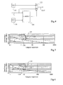
- the abscissa axis corresponds to the duration of the impulse interference, expressed in ⁇ s
- the ordinate axis corresponds to the ratio, expressed in decibels, between the energy level of the impulse interferences and the energy of the COFDM signal.
- curves C1, C2, C3 (respectively C1 ', C2', C3 ') are represented and each delimits a region under the curve corresponding to the impulsive interferences that can be corrected by the demodulator, and a region above the curve corresponding to the impulse interference that can not be corrected by the demodulator and causes therefore in a degradation of the signal finally demodulated.
- the curve C1 (respectively C1 ') represents the limit of tolerance to impulse interference for a demodulator not including a module for suppressing impulse interference.
- Curve C2 (respectively C2 ') represents the impulse interference tolerance limit for a demodulator equipped with a conventional threshold detection pulse interference suppression module as previously described.
- Curve C3 (respectively C3 ') represents the limit of tolerance for pulse inferences for a demodulator equipped with the pulse interference suppression module 11 according to the invention. Analogous curves are obtained for any type of COFDM demodulator comprising an impulse interference suppression module according to the invention.
- Curve C2 (respectively C2 ') comprises a bulge 124 (respectively 124') for impulse interferences of the order of 2 ⁇ s (respectively 10 ⁇ s). This reflects the fact, as previously described, that the threshold detection pulse interference suppression module is effective in suppressing high energy impulse interference, but does not remove low energy impulse interference.
- Curve C3 (respectively C3 ') comprises a vertical straight portion 125 (respectively 125') which corresponds to the theoretical limit of disturbance tolerance that a demodulator can accept. Indeed, it is known that a symbol disturbed by a perturbation whose energy is greater than about 1% of the energy of a symbol can no longer be found correctly. For a 2K modulation, the duration of a useful symbol being 224 ⁇ s, we therefore consider only a pulse interference duration of less than about 2.3 ⁇ s. For an 8K modulation, the duration of a useful symbol being 896 ⁇ s, we therefore consider only an impulse interference of less than about 10 ⁇ s duration.
- the demodulator comprising the impulse interference suppression module according to the invention thus makes it possible to correct an emitted modulated signal disturbed by impulse interference over a greater range of interference durations or interference energy levels than a demodulator comprising a pulse detection interference suppression module.
Landscapes
- Engineering & Computer Science (AREA)
- Computer Networks & Wireless Communication (AREA)
- Signal Processing (AREA)
- Noise Elimination (AREA)
Claims (8)
- Eine Vorrichtung (11) zum Unterdrücken von Pulsinterferenzen, die in einem Signal (IF) enthalten sind, wobei die Vorrichtung einen Schaltkreis (62, 64, 66) zum Detektieren von Pulsinterferenzen, die in einem Signal enthalten sind, aufweist, und einen Schaltkreis (68) zum Korrigieren des Signals, das durch die detektierten Pulsinterferenzen gestört wird, wobei der Detektionsschaltkreis Folgendes aufweist:einen Schaltkreis (62) zum Detektieren eines ersten Koeffizienten (COEFF1), der repräsentativ ist für eine statistische Charakteristik der Variation des Signals über eine erste Zeitperiode;einen Schaltkreis (64) zum Detektieren eines zweiten Koeffizienten (COEFF2), der repräsentativ ist für eine statistische Charakteristik der Variation des Signals über eine zweite Zeitperiode, die länger ist als die erste Zeitperiode; undeinen Vergleichsschaltkreis (66), der den ersten und den zweiten Koeffizienten vergleicht und ein Signal bereitstellt, das anzeigend für die Anwesenheit einer Pulsinterferenz über der ersten Zeitperiode ist, wenn der erste Koeffizient sich klar von dem zweiten Koeffizient unterscheidet,dadurch gekennzeichnet, dass der Schaltkreis (62) zum Bestimmen des ersten Koeffizienten (COEFF1) die Summe der absoluten Werte der aufeinanderfolgenden digitalen Werte bereitstellt, die durch Sampling des Signals (IF) während der ersten Zeitperiode erhalten werden, wobei jeder absolute Wert der einen digitalen Wert aufweist, der größer ist als eine bestimmte Schwelle (SEUIL1), durch eine Gewichtungskonstante (VAL1) ersetzt wird, die größer oder gleich ist als die Schwelle, wobei die Vorrichtung ferner dadurch gekennzeichnet ist, dass der Schaltkreis (64) zum Bestimmen des zweiten Koeffizienten den zweiten Koeffizienten (COEFF2) bestimmt, basierend auf den absoluten Werten der aufeinanderfolgenden digitalen Werte, die durch das Sampling des Signals während der zweiten Zeitperiode erhalten werden.
- Die Vorrichtung nach Anspruch 1, wobei der Schaltkreis (62) zum Bestimmen des ersten Koeffizienten (COEFF1) Folgendes aufweist:einen ersten Eingang, der erste aufeinanderfolgende digitale Werte empfängt, die durch das Sampling des Signals (IF) bereitgestellt werden;einen zweiten Eingang, der zweite aufeinanderfolgende digitale Werte empfängt, die durch das Signalsampling bereitgestellt werden, das in der Zeit, bezüglich der ersten aufeinanderfolgenden digitalen Werte der ersten Zeitperiode, verschoben ist;einen ersten Verarbeitungsschaltkreis (70, 72), der mit dem ersten Eingang verbunden ist und geeignet ist dritte aufeinanderfolgende digitale Werte (OUT1) bereitzustellen, die den absoluten Werten der ersten aufeinanderfolgenden digitalen Werte entsprechen, wobei jeder absolute Wert eines ersten digitalen Wertes, der größer ist als eine Schwelle (SEUIL1) durch die Gewichtungskonstante (VAL1) ersetzt wird;einen zweiten Verarbeitungsschaltkreis (74, 76), der mit dem zweiten Eingang verbunden ist und geeignet ist vierte aufeinanderfolgende digitale Werte (OUT2) bereitzustellen, die den absoluten Werten der zweiten aufeinanderfolgenden digitalen Werte entsprechen, wobei jeder absolute Wert eines zweiten digitalen Wertes, der größer ist als eine Schwelle (SEUIL1) durch die Gewichtungskonstante ersetzt wird;einen Subtraktor (78), der mit dem ersten und dem zweiten Gewichtungsschaltkreis verbunden ist und aufeinanderfolgend fünfte aufeinanderfolgende digitale Werte bereitstellt, die der Subtraktion zwischen den vierten aufeinanderfolgenden digitalen Werten und den dritten aufeinanderfolgenden digitalen Werten entsprechen; undeinen Addierer (78) mit einem ersten Eingang, der die fünften aufeinanderfolgenden digitalen Werte empfängt und mit einem zweiten Eingang, der mit dem Ausgang des Addierers verbunden ist und wobei der Addierer sechste aufeinanderfolgende digitale Werte bereitstellt, die dem ersten Koeffizienten entsprechen.
- Die Vorrichtung nach Anspruch 2, wobei die Gewichtungskonstante (VAL1) größer oder gleich drei Mal der Schwelle (SEUIL1) ist.
- Die Vorrichtung nach Anspruch 1, wobei der Schaltkreis (64) zum Bestimmen des zweiten Koeffizienten (COEFF2) Folgendes aufweist:einen Eingang, der erste aufeinanderfolgende digitale Werte empfängt, die durch Sampling des Signals (IF) bereitgestellt werden;einen Verarbeitungsschaltkreis (74, 82), der mit dem Eingang verbunden ist und geeignet ist zweite aufeinanderfolgende digitale Werte (OUT3) bereitzustellen, die den absoluten Werten der ersten aufeinanderfolgenden digitalen Werte entsprechen, wobei jeder absolute Wert eines ersten digitalen Wertes, der größer ist als eine Schwelle (SEUIL3) durch eine Gewichtungskonstante (VAL3) ersetzt wird, die kleiner oder gleich ist wie die Schwelle;einen Addierer (84) mit einem ersten Eingang, der die zweiten aufeinanderfolgenden digitalen Werte empfängt und mit einem zweiten Eingang, der mit dem Ausgang des Addierers verbunden ist und wobei der Addierer dritte aufeinanderfolgende digitale Werte bereitstellt; undeinen Schaltkreis (92), der die dritten aufeinanderfolgenden digitalen Werte empfängt und vierte aufeinanderfolgende digitale Werte bereitstellt, die dem zweiten Koeffizienten entsprechen, der gleich ist zu den dritten aufeinanderfolgenden digitalen Werten multipliziert mit dem Verhältnis zwischen der ersten Zeitperiode und der zweiten Zeitperiode.
- Die Vorrichtung nach Anspruch 4, wobei der zweite Eingang des Addierers (84) den Nullwert während eines Operationszyklus des Addierers empfängt, nach einer bestimmten Anzahl von aufeinanderfolgenden Operationszyklen gleich der zweiten Zeitperiode.
- Die Vorrichtung nach Anspruch 4, wobei die dritten aufeinanderfolgenden digitalen Werte multipliziert werden mit einem Korrekturkoeffizienten (Corr), der größer oder gleich 2 ist.
- Ein Verfahren zum Unterdrücken von Pulsinterferenzen, die in einem Signal (IF) enthalten sind, wobei das Verfahren einen Schritt des Detektierens von Pulsinterferenzen, die in einem Signal enthalten sind, aufweist, und einen Schritt zum Korrigieren der detektierten Pulsinterferenzen, wobei der Detektionsschritt Folgendes aufweist:einen Schritt zum Detektieren eines ersten Koeffizienten (COEFF1), der repräsentativ ist für eine statistische Charakteristik der Variation des Signals über eine erste Zeitperiode und eines zweiten Koeffizienten (COEFF2), der repräsentativ ist für eine statistische Charakteristik der Variation des Signals über eine zweite Zeitperiode, die größer ist als die erste Zeitperiode; undeinen Schritt des Detektierens der Anwesenheit einer Pulsinterferenz auf dem Signal durch Vergleichen des ersten und zweiten Koeffizienten,dadurch gekennzeichnet, dass der erste Koeffizient (COEFF1) der Summe der absoluten Werte der aufeinanderfolgenden digitalen Werte entspricht, die durch Sampling des Signals (IF) während der ersten Zeitperiode erhalten werden, wobei jeder absolute Wert der einen digitalen Wert aufweist der größer ist als eine bestimmte Schwelle (SEUIL1), durch eine Gewichtungskonstante (VAL1) ersetzt wird, die größer oder gleich ist wie die Schwelle, wobei das Verfahren ferner dadurch gekennzeichnet ist, dass der zweite Koeffizient (COEFF2) bestimmt wird, basierend auf den absoluten Werten der aufeinanderfolgenden digitalen Werte, die durch das Sampling des Signals während der zweiten Zeitperiode erhalten werden.
- Das Verfahren nach Anspruch 7, wobei der zweite Koeffizient (COEFF2) der Summe der absoluten Werte, möglicherweise korrigiert, der aufeinanderfolgenden digitalen Werte entspricht, die durch Sampling des Signals während der zweiten Zeitperiode erhalten werden.
Applications Claiming Priority (2)
| Application Number | Priority Date | Filing Date | Title |
|---|---|---|---|
| FR0450312 | 2004-02-19 | ||
| FR0450312 | 2004-02-19 |
Publications (2)
| Publication Number | Publication Date |
|---|---|
| EP1566935A1 EP1566935A1 (de) | 2005-08-24 |
| EP1566935B1 true EP1566935B1 (de) | 2012-07-25 |
Family
ID=34708049
Family Applications (1)
| Application Number | Title | Priority Date | Filing Date |
|---|---|---|---|
| EP05101201A Expired - Lifetime EP1566935B1 (de) | 2004-02-19 | 2005-02-17 | Vorrichtung und Verfahren zur Unterdrückung von Impulsinterferenzen in einem Signal |
Country Status (2)
| Country | Link |
|---|---|
| US (1) | US7760825B2 (de) |
| EP (1) | EP1566935B1 (de) |
Families Citing this family (6)
| Publication number | Priority date | Publication date | Assignee | Title |
|---|---|---|---|---|
| US8094759B2 (en) * | 2007-03-16 | 2012-01-10 | Xg Technology, Inc. | System and method for broadband pulse detection among multiple interferers using a dynamic filter receiver |
| US8130116B1 (en) * | 2007-08-27 | 2012-03-06 | Daigle Harold S | Mobile telephone tracking system |
| CN101945064B (zh) * | 2010-08-19 | 2013-05-08 | 电子科技大学 | 基于能量扩展的迭代抗多音干扰通信方法 |
| US8761540B2 (en) * | 2011-06-14 | 2014-06-24 | Kabushiki Kaisha Toshiba | Method and system for estimating noise level |
| EP3396398B1 (de) * | 2017-04-27 | 2020-07-08 | Rohde & Schwarz GmbH & Co. KG | Signalkorrekturverfahren, system zur korrektur eines messsignals sowie oszilloskop |
| US11216024B1 (en) | 2021-03-20 | 2022-01-04 | Sitrus Technology Corporation | Referenceless frequency acquisition |
Family Cites Families (21)
| Publication number | Priority date | Publication date | Assignee | Title |
|---|---|---|---|---|
| US3621139A (en) * | 1970-05-11 | 1971-11-16 | North American Rockwell | Data receiver with intersymbol interference correction |
| CA1180141A (en) * | 1980-11-15 | 1984-12-27 | Kenzo Takahashi | Echo canceller system |
| US4392138A (en) * | 1981-01-05 | 1983-07-05 | Motorola, Inc. | Apparatus and method for detecting and inhibiting signals interfering with a Loran C signal |
| NL8402322A (nl) * | 1984-07-23 | 1986-02-17 | Philips Nv | Inrichting voor het detekteren van impulsachtige storingen, en een inrichting voor het onderdrukken van impulsachtige storingen voorzien van een inrichting voor het detekteren van impulsachtige storingen. |
| US4680588A (en) * | 1985-12-05 | 1987-07-14 | Raytheon Company | Radar system with incremental automatic gain control |
| US4789838A (en) * | 1987-03-23 | 1988-12-06 | Cheng Jyi Min | Pulse detection circuit using amplitude and time qualification |
| US4932039A (en) * | 1989-06-08 | 1990-06-05 | The United States Of America As Represented By The Secretary The Navy | Pulse interference canceler of high power out-of-band pulse interference signals |
| FR2676880B1 (fr) * | 1991-05-24 | 1994-12-30 | France Telecom | Analyseur modulaire de trafic de signaux numeriques. |
| FR2689250B1 (fr) * | 1992-03-31 | 1994-05-13 | Thomson Csf | Procede et dispositif de detection de melanges d'impulsions recues par un radar secondaire. |
| TW237587B (de) * | 1993-03-19 | 1995-01-01 | Philips Electronics Nv | |
| JP2814053B2 (ja) * | 1993-12-10 | 1998-10-22 | 日本プレシジョン・サーキッツ株式会社 | 信号記録方法、信号再生方法および信号記録再生方法 |
| DE4344022C2 (de) * | 1993-12-23 | 2003-06-05 | Eads Deutschland Gmbh | Digitales Verfahren zur Detektion zeitlich kurzer Pulse und Anordnung zur Durchführung des Verfahrens |
| JP3627349B2 (ja) * | 1996-02-26 | 2005-03-09 | 松下電器産業株式会社 | ディジタル通信用高周波受信装置 |
| KR100537496B1 (ko) * | 1997-02-19 | 2006-03-23 | 삼성전자주식회사 | 데이터 채널상의 부가형 외란 제거 장치 및 방법 |
| GB0004727D0 (en) * | 2000-02-29 | 2000-04-19 | Renishaw Plc | Machine tool probe with wireless signal transmission |
| US6501607B2 (en) * | 2001-01-10 | 2002-12-31 | Texas Instruments Incorporated | Channel quality monitor (CQM) for digital peak detection (DPD) |
| FR2835136A1 (fr) * | 2002-01-22 | 2003-07-25 | St Microelectronics Sa | Demodulateur cofdm a positionnement optimal de fenetre d'analyse fft |
| US7257740B2 (en) * | 2002-06-10 | 2007-08-14 | Nxp B.V. | Circuit for detecting ground offset of parts of a network |
| DE10233835A1 (de) * | 2002-07-25 | 2004-02-12 | Robert Bosch Gmbh | Verfahren zur Störbefreiung von Messsignalen |
| EP1583306B1 (de) * | 2004-03-10 | 2014-05-07 | St Microelectronics S.A. | Mehrträgerempfänger mit Einschätzung der Zeitvarianz des Kanals |
| FR2868640B1 (fr) * | 2004-03-31 | 2006-06-09 | St Microelectronics Sa | Demodulateur cofdm a positionnement optimal de fenetre d'analyse fft |
-
2005
- 2005-02-17 EP EP05101201A patent/EP1566935B1/de not_active Expired - Lifetime
- 2005-02-17 US US11/060,066 patent/US7760825B2/en active Active
Also Published As
| Publication number | Publication date |
|---|---|
| EP1566935A1 (de) | 2005-08-24 |
| US7760825B2 (en) | 2010-07-20 |
| US20050190869A1 (en) | 2005-09-01 |
Similar Documents
| Publication | Publication Date | Title |
|---|---|---|
| EP0920163B1 (de) | Schätzung des groben Frequenzversatzes in Mehrträgerempfängern | |
| EP0950306B1 (de) | Verfahren und vorrichtung zum formen des beschneidungsrauschens einer mehrträgermodulation | |
| FR2598872A1 (fr) | Systeme de demodulation de signal numerique | |
| EP1583306B1 (de) | Mehrträgerempfänger mit Einschätzung der Zeitvarianz des Kanals | |
| EP3188426B1 (de) | Adaptives verfahren zur anwendung von entstörungsmassnahmen in einem mehrweg-empfänger | |
| FR2904168A1 (fr) | Systeme d'estimation de la qualite de reception d'une transmission numerique. | |
| EP0576359B1 (de) | Verfahren und Einrichtung zur entscheidungsrückgekoppelten Entzerrung für die blockweise Übertragung von Informationssymbolen | |
| EP0767996A1 (de) | Verfahren zur schätzung beziehungsweise korrektur eines restlichen phasenfehlers in einem demodulierten digitalen signal | |
| FR2825552A1 (fr) | Dispositif et procede de demodulation numerique d'un signal recu par selection d'un filtre et recepteur de communication numerique le comportant | |
| EP1566935B1 (de) | Vorrichtung und Verfahren zur Unterdrückung von Impulsinterferenzen in einem Signal | |
| EP1330091B1 (de) | Verfahren zur Selektion einer Position eines FFT-Fensters in einem COFDM-Empfänger | |
| EP0376250B1 (de) | Selbst-adaptive Entzerrungseinrichtung für eine differentielle kohärente Demodulationsanordnung | |
| US7127019B2 (en) | Methods and apparatus for implementing multi-tone receivers | |
| EP0549445A1 (de) | Verfahren zur Übertragung von Referenzsignalen in einem Mehrträgerdatenübertragungssystem | |
| EP1810470B1 (de) | Verfahren zum empfang eines mehrträgersignals, das wenigstens zwei schätzungen eines kanals verwendet und entsprechender empfänger | |
| CA2060413C (fr) | Procede de detection de signal perturbateur pour demodulateur de donnees numeriques et dispositif de mise en oeuvre d'un tel procede | |
| FR2742613A1 (fr) | Procede d'evaluation d'un facteur de qualite representatif d'un canal de transmission d'un signal numerique, et recepteur correspondant | |
| FR2679721A1 (fr) | Procede d'egalisation adaptative reduisant l'interference intersymbole, et dispositif de reception et application correspondants. | |
| US7295144B1 (en) | Quantizer responsive to noise level for a wireless communications system | |
| EP1826974B1 (de) | Verfahren und Gerät zur Schätzung der Kanalübertragungsfunktion für einen COFDM Demodulator | |
| EP1826973B1 (de) | Verfahren und Gerät zur Schätzung der Übertragungsfunktion des Kanals für einen COFDM-Demodulator | |
| EP1438815B1 (de) | Zwischensymbolstörungslöscher | |
| FR2825550A1 (fr) | Dispositif et procede de demodulation numerique d'un signal recu par selection d'un filtre et recepteur de communication numerique le comportant | |
| FR3112915A1 (fr) | Procédé d’estimation d’un signal interférent, procédé d’atténuation d’un signal interférent contenu dans un signal réceptionné et système de réception | |
| EP2175599A1 (de) | Verfahren zur Unterdrückung impulsiver Störungen |
Legal Events
| Date | Code | Title | Description |
|---|---|---|---|
| PUAI | Public reference made under article 153(3) epc to a published international application that has entered the european phase |
Free format text: ORIGINAL CODE: 0009012 |
|
| AK | Designated contracting states |
Kind code of ref document: A1 Designated state(s): AT BE BG CH CY CZ DE DK EE ES FI FR GB GR HU IE IS IT LI LT LU MC NL PL PT RO SE SI SK TR |
|
| AX | Request for extension of the european patent |
Extension state: AL BA HR LV MK YU |
|
| AKX | Designation fees paid | ||
| 17P | Request for examination filed |
Effective date: 20060222 |
|
| RBV | Designated contracting states (corrected) |
Designated state(s): DE FR GB IT |
|
| REG | Reference to a national code |
Ref country code: DE Ref legal event code: 8566 |
|
| 17Q | First examination report despatched |
Effective date: 20110616 |
|
| GRAP | Despatch of communication of intention to grant a patent |
Free format text: ORIGINAL CODE: EPIDOSNIGR1 |
|
| GRAS | Grant fee paid |
Free format text: ORIGINAL CODE: EPIDOSNIGR3 |
|
| GRAA | (expected) grant |
Free format text: ORIGINAL CODE: 0009210 |
|
| AK | Designated contracting states |
Kind code of ref document: B1 Designated state(s): DE FR GB IT |
|
| REG | Reference to a national code |
Ref country code: GB Ref legal event code: FG4D Free format text: NOT ENGLISH |
|
| REG | Reference to a national code |
Ref country code: DE Ref legal event code: R096 Ref document number: 602005035256 Country of ref document: DE Effective date: 20120920 |
|
| PG25 | Lapsed in a contracting state [announced via postgrant information from national office to epo] |
Ref country code: IT Free format text: LAPSE BECAUSE OF FAILURE TO SUBMIT A TRANSLATION OF THE DESCRIPTION OR TO PAY THE FEE WITHIN THE PRESCRIBED TIME-LIMIT Effective date: 20120725 |
|
| PLBE | No opposition filed within time limit |
Free format text: ORIGINAL CODE: 0009261 |
|
| STAA | Information on the status of an ep patent application or granted ep patent |
Free format text: STATUS: NO OPPOSITION FILED WITHIN TIME LIMIT |
|
| 26N | No opposition filed |
Effective date: 20130426 |
|
| REG | Reference to a national code |
Ref country code: DE Ref legal event code: R097 Ref document number: 602005035256 Country of ref document: DE Effective date: 20130426 |
|
| GBPC | Gb: european patent ceased through non-payment of renewal fee |
Effective date: 20130217 |
|
| PG25 | Lapsed in a contracting state [announced via postgrant information from national office to epo] |
Ref country code: GB Free format text: LAPSE BECAUSE OF NON-PAYMENT OF DUE FEES Effective date: 20130217 |
|
| PGFP | Annual fee paid to national office [announced via postgrant information from national office to epo] |
Ref country code: FR Payment date: 20140221 Year of fee payment: 10 |
|
| PGFP | Annual fee paid to national office [announced via postgrant information from national office to epo] |
Ref country code: DE Payment date: 20140122 Year of fee payment: 10 |
|
| REG | Reference to a national code |
Ref country code: DE Ref legal event code: R119 Ref document number: 602005035256 Country of ref document: DE |
|
| REG | Reference to a national code |
Ref country code: FR Ref legal event code: ST Effective date: 20151030 |
|
| PG25 | Lapsed in a contracting state [announced via postgrant information from national office to epo] |
Ref country code: DE Free format text: LAPSE BECAUSE OF NON-PAYMENT OF DUE FEES Effective date: 20150901 |
|
| PG25 | Lapsed in a contracting state [announced via postgrant information from national office to epo] |
Ref country code: FR Free format text: LAPSE BECAUSE OF NON-PAYMENT OF DUE FEES Effective date: 20150302 |