FIELD OF THE INVENTION
The present invention relates to a sensor device having a sensor chip and a
bonding wire fixed by a binding material on a substrate used as a case, a circuit
board or a lead frame.
BACKGROUND OF THE INVENTION
A conventional sensor device is disclosed in, for example, US Patent No.
6,593,663, the contents of which are incorporated herein by reference. The
acceleration sensor includes a sensor chip for sensing acceleration by a sensor
portion disposed on a substrate made of silicon or the like, and a circuit chip as a
base substrate mounting the sensor chip thereon by using an adhesive film.
In this type of conventional sensor device, the sensor chip is connected to
the substrate by a bonding wire. That is, the sensor chip is wire-bonded to the
substrate.
The conventional sensor device described above uses a binding material
made of silicon resin or the like with minimum elasticity to protect the sensor chip
fixed on the substrate from stress. In this manner, the sensitivity of the sensor
device is improved.
However, the modulus of elasticity of the binding material, e.g. an adhesive
film, has to be 1 MPa or more in order to stably support the sensor chip when the
wire is bonded on the chip.
Therefore, the sensitivity of the conventional sensor device is restricted by
the modulus of elasticity of the binding material. In other words, there is a trade-off
between the sensitivity of the sensor and the elasticity of the binding material in the
conventional sensor device.
In other words, it is necessary to use a less elastic binding material in order
to further increase the sensitivity of the sensor device. This is because the stress
transfer from the substrate to the sensor chip has to be decreased by using less
elastic binding material, for example, with the modulus of elasticity being 1 MPa or
less.
The less elastic binding material, however, causes a problem in a wire
bonding process. That is, the wire bonding process can't be stably conducted when
the binding material is too low in the modulus of elasticity (too soft).
SUMMARY OF THE INVENTION
In view of the above-described problems, it is an object to provide a sensor
device including a sensor chip and a bonding wire fixed on a substrate by a binding
material suitable for both increased sensitivity and a wire bonding process.
Accordingly, a sensor device of the present embodiment includes a sensor
chip that is fixed on a substrate by a binding material and has a bonding wire
connected thereto. A binding material that loses elasticity on application of energy
in comparison to pre-energized state is used.
That is, the binding material is made less elastic when energized than in the
pre-energized state. The binding material is elastic enough to stably support the
sensor chip on the substrate for a wire bonding process in a pre-energized state.
The binding material is then energized to be less elastic after the wire bonding
process.
Therefore, the elasticity of the binding material becomes much lower than the
one being used in the conventional art in terms of preventing stress transfer to the
sensor chip.
Therefore, the sensor device having a sensor chip being fixed on a substrate
by a binding material and having a bonding wire connected thereto can be wire-bonded
and can also have an increased sensitivity.
In the sensor device of the present embodiment, the binding material is has
the following characteristics. That is, the energized binding material is functional as
a cushion with air voids contained therein. In the energizing process, heat is used
as a source of energy. The binding material is made of an adhesive containing a
foaming agent that evaporates on application of heat.
After the sensor chip is fixed on the substrate and wire-bonded, the binding
material is heated to evaporate the foaming agent in the adhesive for forming air
voids. As a result, the heated binding material becomes less elastic because of the
air voids contained therein are functional as a cushion.
In the sensor device, the foaming agent is made of either of an
Azodicarbonamide, a Di-nitrosopentamethylenetetramin, a Benzenesulphonyl
hydrazide or a mixture of these materials.
BRIEF DESCRIPTION OF THE DRAWINGS
Other objects, features and advantages of the present invention will become
more apparent from the following detailed description made with reference to the
accompanying drawings, in which:
DETAILED DESCRIPTION OF THE PREFERRED EMBODIMENTS
The following is a description of preferred embodiments with reference to
drawings. Same numerals in the drawings designate the same or equivalent thing in
the drawings for brevity of explanation.
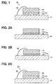
An acceleration sensor S1 according to a preferred embodiment is illustrated
in FIG. 1. The acceleration sensor S1 may be implemented within, for example, a
driving control system on an automotive vehicle, although the acceleration sensor is
not necessarily limited to being implemented within such a device.
A substrate 10 shown in FIG. 1 is a component such as a case, a housing, a
printed circuit substrate/ceramic substrate or a lead frame may be utilized. A
material for the substrate 10 may be, though not necessarily limited, resin, ceramic or
metal. When the substrate 10 is used as a part of the case or the housing, the case
or the housing has a conducting portion to be connected to a bonding wire 40.
The substrate 10 has a sensor chip 20 mounted thereon. The sensor chip
20 is attached to and fixed to the substrate 10 by a binding material 30.
The sensor chip 20 and the substrate 10 are electrically connected by the
bonding wire 40. The bonding wire 40 is formed in a wire bonding process that uses
gold, aluminum or the like as a material of the bonding wire 40.
The sensor chip 20 is, in this case, used as an acceleration sensor. A beam
structure with a comb portion of well-known type is formed on a silicon substrate or
the like to pick up changes of an interelectrode capacitance (electric signal) between
a movable electrode and a fixed electrode being proportional to acceleration.
The electric signal from the sensor chip 20 is, for example, converted by a
C/V conversion circuit on the substrate 10 to variations of voltage, and then is output
to an external circuit as an acceleration signal through the bonding wire 40 after
being treated in processes such as amplification, adjustment and the like.
The binding material 30 that attaches the sensor chip 20 to the substrate 10
is made of a material that reduces elasticity on an application of energy, such as heat,
light or the like, while fixing the sensor chip 20 to the substrate 10, that is, while
maintaining the functionality of an adhesive.
In a finished state of the acceleration sensor S1, the binding material 30 is
already energized to have the modulus of elasticity of, for example, approximately 0.5
MPa, being much lower than a material used in a conventional sensor device.
The binding material 30 is, as shown in FIG. 1, functional as a cushion
because of voids 31 of air contained therein. In other words, the binding material of
the conventional sensor device is homogeneous without any void contained therein,
while the binding material 30 in the present embodiment is heterogeneous with the
voids 31 contained therein to be functional as a cushion.
The binding material 30 is made of, for example, an adhesive 32 containing a
foaming agent 31 a that evaporates on application of heat (as shown in FIG. 2A).
The binding material 30 of this kind contains the voids 31 when heat is applied to
evaporate the foaming agent 31 a in the adhesive 32.
The foaming agent 31 a in the binding material 30 is made of, for example, a
material such as an Azodicarbonamide, a Di-nitrosopentamethylenetetramin, a
Benzenesulphonyl hydrazide, a mixture of these materials or the like. The adhesive
32 is, for example, a thermosetting resin adhesive made of a silicon type resin with
the modulus of elasticity of approximately 1 MPa.
The foaming agent 31a is, for example, contained in the adhesive 32 as a
powder. A mixture ratio having a preferable post-heating elasticity can be easily
determined by those who are skilled in the art, based on the type and the elasticity of
the adhesive 32.
A method for manufacturing the acceleration sensor S1 will now be explained
with reference to FIGS. 2A to 2C. FIGS. 2A to 2C are schematical cross-sectional
views of a manufacturing process of the acceleration sensor S1 illustrating how
components are structured.
First, as shown in FIG. 2A, the binding material 30 is placed on the substrate
10. The binding material 30 made of the adhesive 32 containing the powdered
foaming agent 31 a is, as described above, applied to the substrate 10 by a dispense
method or the like.
In this case, the evaporative foaming agent 31 a on application of heat, being
made of a material such as an Azodicarbonamide, a Di-nitrosopentamethylenetetramin,
a Benzenesulphonyl hydrazide or the like, is mixed in
the silicon type adhesive 32 with the modulus of elasticity of 1 MPa.
Next, the sensor chip 20 is placed on the binding material 30, and is treated
in a heating process and the like to harden the binding material 30. At this stage,
the adhesive 32 in the binding material 30 hardens while the foaming agent 31 a stays
in a solid state (powder).
Then, as shown in FIG. 2B, the wire bonding process is executed. The
bonding wire 40 is bonded to the sensor chip 20 and the substrate 10 to electrically
connect the chip 20 and the substrate 10. The foaming agent 31 a is still in a solid
state (powder).
Further, as shown in FIG. 2C, the chip 20 fixed on the substrate by the
binding material 30 is heated, for example, to 200°C. In this process, the foaming
agent 31 a in the adhesive 32 evaporates and forms the voids 31. This completes
the manufacturing process of the acceleration sensor S1 in this embodiment.
In this embodiment, the sensor device S1, including the sensor chip 20 being
fixed on the substrate 10 by the binding material 30 and having the bonding wire 40
connected thereto, is characterized by the binding material 30 that reduces elasticity
when energy is applied to the material 30.
The binding material 30 fulfills the following requirements because the
material 30 reduces elasticity when energy is applied. That is, the material 30 is
elastic (hard enough) to stably support the sensor chip 20 fixed on the substrate 10 in
the wire bonding process. The binding material 30 reduces elasticity after the wire
bonding process on application of energy.
Therefore, the modulus of elasticity of the binding material 30 is 1 MPa or
more in the wire bonding process, and the modulus of elasticity is reduced to
approximately 0.5 MPa after the wire bonding process.
In this embodiment, the elasticity of the binding material 30 can be reduced
to a level that is not sufficiently elastic (hard enough) to conduct the wire bonding.
In other words, the elasticity of the binding material 30 can be lowered to an
unprecedented level, thereby also lowering the stress transfer level to the sensor chip
20.
Therefore, in the sensor device of the present embodiment, including the
sensor chip 20 being fixed on the substrate 10 by the binding material 30 and having
the bonding wire 40 connected thereto, the sensor chip 20 can be wire-bonded while
sensitivity of the sensor device can be increased.
The binding material 30 of the sensor device S1 in this embodiment is being
functional as a cushion by containing the voids 31 of air as shown in FIG. 1.
More practically, the binding material 30 is made of the silicon type adhesive
32 containing the foaming agent 31 a such as an Azodicarbonamide, a Di-nitrosopentamethylenetetramin,
a Benzenesulphonyl hydrazide or a mixture of these
materials to provide the required characteristics described above.
The above-described binding material 30 forms the voids 31 by evaporation
of the foaming agent 31 a in the adhesive 32 on application of heat to the material 30
after the sensor chip 20 is fixed on and wire-bonded to the substrate 10.
Therefore, the binding material 30 preferably becomes heterogeneous and
functional as a cushion after heating because of the voids 31 of air formed therein.
As a result, the elasticity of the material 30 reduces.
The extremely low elasticity of the binding material 30 required in this
embodiment can only be achieved, for example, by using a gel type material when
the material is homogeneous without voids as in the conventional art. In this case,
the elasticity is too low to stably conduct a wire bonding process on a sensor chip.
In this embodiment, the foaming agent 31 a in the adhesive 32 evaporates on
application of heat to form the voids 31. The voids 31 may also be formed by a
light-sensitive foaming agent or the like.
(Other embodiment)
In the above embodiment, the binding material with an extremely low
elasticity is provided by forming voids on application of heat or light. The binding
material with this characteristic, reduction of elasticity on application of energy, is not
necessarily provided in this manner.
For example, an adhesive that reduces elasticity on application of heat, light
or the like, or an adhesive containing the material having that kind of characteristics
may be used as the binding material. By using this kind of adhesive, the binding
material of the present embodiment is suitably prepared because the elasticity of the
adhesive is reduced by a chemical reaction or the like to an extremely low level on
application of energy (such as heat or the like).
The binding material may also be made of an adhesive having an ingredient
that evaporates or decomposes on application of heat, light or the like. The
adhesive may include a material having this kind of characteristics as a mixture.
The binding material of this kind will have spaces similar to voids formed by
evaporation or decomposition on application of energy. The void-like space will be
functional as a cushion in the binding material to appropriately provide the extremely
low elasticity required in the present invention.
In the present invention, the energy to be applied to the binding material may
be, for example, an ultrasonic wave or the like. A binding material having a
substance that decomposes on application of the ultrasonic wave will also be
appropriately used in this embodiment.
An acceleration sensor is taken as an example in the explanation of the
present embodiment. However, the present embodiment may also be applied to
other types of sensors, such as an angular velocity sensor, a pressure sensor, a
temperature sensor or a light sensor. That is, the sensor chip 20 may be an angular
velocity sensing element, a pressure sensing element, a temperature sensing
element or a light sensing element in the embodiment described above.