EP1565807B1 - Zugeordnete anzeigevorrichtung mit näherungsdetektion - Google Patents
Zugeordnete anzeigevorrichtung mit näherungsdetektion Download PDFInfo
- Publication number
- EP1565807B1 EP1565807B1 EP03796063.0A EP03796063A EP1565807B1 EP 1565807 B1 EP1565807 B1 EP 1565807B1 EP 03796063 A EP03796063 A EP 03796063A EP 1565807 B1 EP1565807 B1 EP 1565807B1
- Authority
- EP
- European Patent Office
- Prior art keywords
- electrode
- electrodes
- dedicated
- disposed
- opposite
- Prior art date
- Legal status (The legal status is an assumption and is not a legal conclusion. Google has not performed a legal analysis and makes no representation as to the accuracy of the status listed.)
- Expired - Lifetime
Links
Images

Classifications
-
- G—PHYSICS
- G06—COMPUTING OR CALCULATING; COUNTING
- G06F—ELECTRIC DIGITAL DATA PROCESSING
- G06F3/00—Input arrangements for transferring data to be processed into a form capable of being handled by the computer; Output arrangements for transferring data from processing unit to output unit, e.g. interface arrangements
- G06F3/01—Input arrangements or combined input and output arrangements for interaction between user and computer
- G06F3/03—Arrangements for converting the position or the displacement of a member into a coded form
- G06F3/041—Digitisers, e.g. for touch screens or touch pads, characterised by the transducing means
- G06F3/0412—Digitisers structurally integrated in a display
-
- G—PHYSICS
- G06—COMPUTING OR CALCULATING; COUNTING
- G06F—ELECTRIC DIGITAL DATA PROCESSING
- G06F3/00—Input arrangements for transferring data to be processed into a form capable of being handled by the computer; Output arrangements for transferring data from processing unit to output unit, e.g. interface arrangements
- G06F3/01—Input arrangements or combined input and output arrangements for interaction between user and computer
- G06F3/03—Arrangements for converting the position or the displacement of a member into a coded form
- G06F3/041—Digitisers, e.g. for touch screens or touch pads, characterised by the transducing means
- G06F3/044—Digitisers, e.g. for touch screens or touch pads, characterised by the transducing means by capacitive means
- G06F3/0443—Digitisers, e.g. for touch screens or touch pads, characterised by the transducing means by capacitive means using a single layer of sensing electrodes
Definitions
- the invention relates to a dedicated display device comprising proximity detection means. Such devices are used in particular for the production of communication terminals of the type enabling an operator to transmit and receive information in the context of a friendly exchange with a processor.
- the invention finds particular application for the screens of interactive terminals having dedicated liquid crystal displays.
- Dedicated screen means a screen comprising at least one or more pictograms fixed during the design of the screen, as for example described in the documents EP 0 345 029 A , US 4,224,615 A and FR 2 198 677 A .
- Such screens have two plates, at least one of which is transparent. Between these plates liquid crystal molecules are available. To excite the liquid crystal molecules and change the polarity of a light beam passing through them, the screen comprises transparent electrodes located on the internal faces of the two plates. In the dedicated screens, in order to simplify the routing of electrode connection pads, it is known to make the electrodes of each plate so that all the pictograms are found identically on the two electrodes facing each other. others.
- the dedicated screens are usually made tactile by placing on the device one or more transparent tactile contact layers or capacitive, inductive or equivalent, as for example described in the documents EP 1 220 140 A and US 4,380,040A .
- the device can then be used to delimit support zones of this layer according to a desired composition.
- the support on the layer is usually done by an operator's finger.
- the disadvantages associated with these known methods relate to the cost of the sensitive component added to the screen and the fact that the visual information provided by the device is inevitably altered by the reported tactile layers.
- the application of the known principle to dedicated displays has a number of disadvantages in that it does not allow to simply adjust the size of the counter-electrodes to different shapes and number of dedicated pictograms associated with a touch zone.
- the routing of the power supply pads of each counterelectrode touch can be made very difficult because of the many power ranges of said pictograms associated with and against the same counter-sensitive electrode.
- the aim of the invention is to overcome these problems by proposing a dedicated tactile screen without a reported tactile layer.
- the invention relates to a display device, the surface of the device being made tactile, the device comprising a first dedicated part comprising two insulating plates, a layer of material having electro-optical properties able to make visible any or part of its surface under the effect of an electrical control signal, the layer being disposed between the two plates, at least a first electrode having the form of a pictogram, the first electrode being disposed on a face of a insulating plates, a second electrode disposed on one face of the other insulating plate facing at least one first electrode, characterized in that the second electrode is used as a sensitive element of the tactile surface of the device by capacitive effect obtained by placing a finger of a user on the device facing the second electrode, the capacitor being created between the finger and the second electrode, in that the surface of the second electrode is at least 9 mm 2 , and in that the surface of the second electrode is greater than or equal to the surface area or the sum of the surfaces of the at least one facing electrode.
- the dedicated display devices are made using static or low-multiplexed liquid crystal displays. They make it possible to display predetermined pictograms during the design of the device.
- static or low-multiplexed displays it is known to connect the counter-electrodes together in groups directly on the plate supporting them, in order to simplify the routing and the number of outputs. It is obvious that this arrangement does not make it possible to produce a tactile display in which it is desired to be able to access each sensitive counterelectrode.
- the display device shown on the figure 1 has two insulating plates 1 and 2 arranged one above the other. At least one of the two plates 1 or 2 is transparent.
- the device also comprises a layer 3 made of a material having electro-optical properties capable of transmitting or not light radiation under the effect of electrical excitation. This material comprises for example liquid crystal.
- the layer 3 is disposed between the two plates 1 and 2.
- the device comprises two first electrodes 4 and 5 having for example the form of a pictogram and being disposed on a face 6 of the plate 2.
- the device further comprises a second electrode 7 disposed on one face 8 of the other insulating plate 1.
- the second electrode 7 is also called against electrode.
- the second electrode 7 is disposed opposite the first two electrodes 4 and 5 so that a control signal applied between one of the first electrodes and the second electrode 7 modifies the state of the liquid crystal between the electrodes.
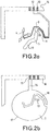
- the figure 2a represents an example of a pictogram made using the electrodes 4 and 5.
- the pictogram of the electrode 4 represents three intersecting arrows and the pictogram of the electrode 5 represents a seated human silhouette. These two pictograms can represent for example the state of ventilation in a motor vehicle.
- the electrode 4 is electrically connected by a strip 9 to a connection pad 10. The same applies to the electrode 5 which is connected by a strip 11 to a connection pad 12.
- the pads 10 and 12 make it possible to apply to the electrodes 4 and 5 the control signal of the device.
- the pads 10 and 12 are located on an edge 16 of the device.
- the electrodes are generally made by etching.
- the etching mask of the counter electrode is made from a mirror image of the etching mask of the first electrodes 4 and 5 to which the mirror images of the first electrodes are connected. electrodes 4 and 5 by narrow width ranges. This way of producing the counterelectrode is unsuitable for producing a display device whose surface is made tactile according to the invention.
- the figure 2b represents the electrode 7 and its electrical connection range 14.
- the range 14 is used to supply the electrode 7 by a stud 15 located on the edge 16 of the device.
- an outer contour 17 of the electrode 7 is substantially oval.
- the electrode 7 When the electrode 7 is placed facing the electrodes 4 and 5, the latter are located inside the contour 17. In other words, the electrode 7 completely covers the electrodes 4 and 5.
- the surface of the electrode 7 is greater than or equal to the sum of the surfaces of the electrodes 4 and 5.
- the electrode 7 must have an area of at least 9 mm 2.
- the capacitive effect is obtained by placing a finger of a user on the device facing the electrode 7. A capacitance is then created between the electrode 7 and the finger.
- the presence of the finger can be detected by analyzing a possible weakening of the high frequency signal due to the existence of the capacitance created between the finger and the electrode 7. Tests have shown that if the surface of the electrode 7 is less than 9 mm 2 , the attenuation of the high signal frequency is so low that it is almost impossible to detect.
- a high frequency electrical signal for example 2MHz
- the pattern of the second electrode 7 substantially covers a circle of at least 9 mm in diameter.
- the counter electrode 7 By producing the counter electrode 7 with a pattern different from those used for the first electrodes 4 and 5, this allows the designer of the device to carry out any form of pictogram forming the pattern of the first electrodes 4 and 5 without worrying about a any minimum area to ensure the proximity detection of a finger of the operator.
- a filiform pictogram can be associated with a counter electrode whose contour is substantially convex. The display is given by the shape of the pictogram and the proximity detection is made possible by the substantially convex shape of the counter electrode.
- the electrode 7 is cut off with respect to the areas 9 and 10.
- the change in state of the liquid crystal is obtained by applying a low frequency control signal, for example at 100 Hz, between on the one hand the electrode 7 and on the other hand at least one of the electrodes 4 or 5.
- the plates 9 and 11 are partly facing the electrode 7 or more precisely inside the contour 17 of the electrode 7. 7 fully occupies the surface located within the contour 17, the portions of the beaches 9 and 11 facing the electrode 7 are then visible at the same time as the pictograms formed by the electrodes 4 and 5.
- the electrode 7 is diverted next to the ranges.
- a clipping path 18 is clearly visible on the figure 2b .
- the device comprises several counter-electrodes (7).
- each is supplied separately. More specifically, each has its own range 14 each terminating in a separate pad 15.
- the device comprises two parts.
- a first part is dedicated as described above and a second part is non dedicated.
- This second part is advantageously arranged in the form of a matrix addressing by rows and columns. This two-part arrangement is described in the European patent EP 0 306 403 .
Landscapes
- Engineering & Computer Science (AREA)
- General Engineering & Computer Science (AREA)
- Theoretical Computer Science (AREA)
- Human Computer Interaction (AREA)
- Physics & Mathematics (AREA)
- General Physics & Mathematics (AREA)
- Position Input By Displaying (AREA)
- Devices For Indicating Variable Information By Combining Individual Elements (AREA)
- Switches That Are Operated By Magnetic Or Electric Fields (AREA)
Claims (6)
- Anzeigevorrichtung, wobei die Oberfläche der Vorrichtung berührungsempfndlich gestaltet ist, die Vorrichtung umfassend einen ersten dedizierten Teil umfassend zwei Isolierplatten (1, 2), eine Schicht (3) aus einem Material, das elektrooptische Eigenschaften aufweist, die in der Lage sind, ihre gesamte oder teilweise Oberfläche unter der Wirkung eines elektrischen Steuersignals sichtbar zu machen, wobei die Schicht (3) zwischen den zwei Platten (1, 2) angeordnet ist, mindestens eine erste Elektrode (4, 5), die die Form eines Piktogramms hat, wobei die erste Elektrode (4, 5) auf einer Seite (6) einer (2) der Isolierplatten angeordnet ist, eine zweite Elektrode (7), die auf einer Seite (8) der anderen (1) Isolierplatte gegenüber der mindestens ersten Elektrode (4, 5) angeordnet ist,
dadurch gekennzeichnet, dass die zweite Elektrode (7) als sensitives Element der berührungsempfindlichen Oberfläche der Vorrichtung durch kapazitive Wirkung verwendet wird, die erlangt wird, indem ein Finger eines Benutzers auf die Vorrichtung gegenüber der zweiten Elektrode (7) aufgelegt wird, wobei die Kapazität zwischen dem Finger und der zweiten Elektrode (7) geschaffen wird, dass die Oberfläche der zweiten Elektrode (7) mindestens 9 mm2 ist,
und dass die Oberfläche der zweiten Elektrode (7) größer als oder gleich wie die Oberfläche oder die Summe von Oberflächen der ersten Elektrode(n) (4, 5) gegenüber ist. - Vorrichtung nach Anspruch 1, dadurch gekennzeichnet, dass die erste Elektrode (4, 5) elektrisch durch einen Bereich (9, 11) versorgt wird, in dem die zweite Elektrode (7) gegenüber dem Bereich (9, 11) profiliert ist.
- Vorrichtung nach einem der vorherigen Ansprüche, dadurch gekennzeichnet, dass sie mehrere zweite Elektroden (7) umfasst, und dass jede zweite Elektrode (7) separat versorgt wird.
- Vorrichtung nach einem der vorherigen Ansprüche, dadurch gekennzeichnet, dass das Muster der zweiten Elektrode (7) im Wesentlichen einen Kreis mit einem Durchmesser von mindestens 9 mm abdeckt.
- Vorrichtung nach einem der vorherigen Ansprüche, dadurch gekennzeichnet, dass sie einen zweiten nicht dezidierten Teil umfasst.
- Vorrichtung nach Anspruch 5 dadurch gekennzeichnet, dass der zweite nicht dedizierte Teil in Form einer Matrix mit Adressierung nach Reihen und Spalten angeordnet ist.
Applications Claiming Priority (3)
| Application Number | Priority Date | Filing Date | Title |
|---|---|---|---|
| FR0215068A FR2847996B1 (fr) | 2002-11-28 | 2002-11-28 | Dispositif d'affichage dedie a detection de proximite |
| FR0215068 | 2002-11-28 | ||
| PCT/EP2003/050903 WO2004049269A2 (fr) | 2002-11-28 | 2003-11-27 | Dispositif d’affichage dedie a detection de proximite |
Publications (2)
| Publication Number | Publication Date |
|---|---|
| EP1565807A2 EP1565807A2 (de) | 2005-08-24 |
| EP1565807B1 true EP1565807B1 (de) | 2017-11-01 |
Family
ID=32309858
Family Applications (1)
| Application Number | Title | Priority Date | Filing Date |
|---|---|---|---|
| EP03796063.0A Expired - Lifetime EP1565807B1 (de) | 2002-11-28 | 2003-11-27 | Zugeordnete anzeigevorrichtung mit näherungsdetektion |
Country Status (6)
| Country | Link |
|---|---|
| US (1) | US7876308B2 (de) |
| EP (1) | EP1565807B1 (de) |
| CN (1) | CN100409158C (de) |
| AU (1) | AU2003298329A1 (de) |
| FR (1) | FR2847996B1 (de) |
| WO (1) | WO2004049269A2 (de) |
Families Citing this family (1)
| Publication number | Priority date | Publication date | Assignee | Title |
|---|---|---|---|---|
| FR2941073B1 (fr) * | 2009-01-15 | 2011-04-08 | Peugeot Citroen Automobiles Sa | Dispositif d'interfacage homme/machine a afficheur lcd a segments, pour le controle tactile modulable de fonctions d'equipements |
Family Cites Families (18)
| Publication number | Priority date | Publication date | Assignee | Title |
|---|---|---|---|---|
| DD105372A1 (de) * | 1972-09-06 | 1974-04-12 | ||
| US4161766A (en) * | 1977-05-23 | 1979-07-17 | General Electric Company | Laminated capacitive touch-pad |
| US4233593A (en) * | 1978-06-12 | 1980-11-11 | General Electric Company | Capacitive touch control and display |
| US4379287A (en) * | 1978-08-08 | 1983-04-05 | Robertshaw Controls Company | Capacitive switch and panel |
| US4224615A (en) * | 1978-09-14 | 1980-09-23 | Texas Instruments Incorporated | Method of using a liquid crystal display device as a data input device |
| CA1152603A (en) * | 1979-09-28 | 1983-08-23 | Bfg Glassgroup | Capacitive systems for touch control switching |
| EP0079711A3 (de) * | 1981-11-16 | 1984-10-03 | The Secretary of State for Defence in Her Britannic Majesty's Government of the United Kingdom of Great Britain and | Berührungsempfindlicher Schalter |
| FR2620254B1 (fr) | 1987-09-04 | 1993-02-05 | Thomson Csf | Dispositif de visualisation a ecran plat avec affichage sous commande de l'operateur |
| FR2630851B1 (fr) * | 1988-04-28 | 1994-02-04 | Sfena | Afficheur a surface tactile incorporee, notamment pour la realisation d'un terminal de communication |
| DE68918759T2 (de) * | 1988-06-01 | 1995-05-18 | Raychem Corp | Schalter mit einem "NCAP" Flüssigkristall. |
| US5572205A (en) * | 1993-03-29 | 1996-11-05 | Donnelly Technology, Inc. | Touch control system |
| KR950009318A (ko) * | 1993-09-03 | 1995-04-21 | 미타라이 하지메 | 표시장치 |
| JPH08160401A (ja) * | 1994-12-02 | 1996-06-21 | Sony Corp | プラズマアドレス表示素子及びその製造方法 |
| US6204839B1 (en) * | 1997-06-27 | 2001-03-20 | Compaq Computer Corporation | Capacitive sensing keyboard and pointing device |
| CN1119782C (zh) * | 1999-08-12 | 2003-08-27 | 友达光电股份有限公司 | 等离子体显示装置 |
| EP1220140A1 (de) * | 2000-12-27 | 2002-07-03 | Asulab S.A. | Verfahren zur Erkennung von auf einer Erfassungsfläche handgeschriebenen Zeichen und Vorrichtung zur Ausführung dieses Verfahrens |
| KR20050026079A (ko) * | 2002-08-01 | 2005-03-14 | 코닌클리즈케 필립스 일렉트로닉스 엔.브이. | 터치 감지 디스플레이 장치 |
| US7352355B2 (en) * | 2002-10-28 | 2008-04-01 | Delphi Technologies, Inc. | Transparent overlay input device |
-
2002
- 2002-11-28 FR FR0215068A patent/FR2847996B1/fr not_active Expired - Lifetime
-
2003
- 2003-11-27 WO PCT/EP2003/050903 patent/WO2004049269A2/fr not_active Ceased
- 2003-11-27 CN CNB2003801043150A patent/CN100409158C/zh not_active Expired - Fee Related
- 2003-11-27 AU AU2003298329A patent/AU2003298329A1/en not_active Abandoned
- 2003-11-27 EP EP03796063.0A patent/EP1565807B1/de not_active Expired - Lifetime
- 2003-11-27 US US10/535,673 patent/US7876308B2/en not_active Expired - Fee Related
Non-Patent Citations (1)
| Title |
|---|
| None * |
Also Published As
| Publication number | Publication date |
|---|---|
| US20060238512A1 (en) | 2006-10-26 |
| AU2003298329A1 (en) | 2004-06-18 |
| US7876308B2 (en) | 2011-01-25 |
| FR2847996A1 (fr) | 2004-06-04 |
| CN100409158C (zh) | 2008-08-06 |
| CN1717647A (zh) | 2006-01-04 |
| AU2003298329A8 (en) | 2004-06-18 |
| EP1565807A2 (de) | 2005-08-24 |
| WO2004049269A2 (fr) | 2004-06-10 |
| FR2847996B1 (fr) | 2005-10-07 |
| WO2004049269A3 (fr) | 2004-11-18 |
Similar Documents
| Publication | Publication Date | Title |
|---|---|---|
| US10324320B2 (en) | Display apparatus and tiled display device including the same | |
| EP2073108B1 (de) | Touchscreen mit kapazitiven Berührungszonen | |
| EP0872759B1 (de) | Flüssigkristallanzeige-Vorrichtung für einen farbigen Bildschirm | |
| FR2957685A1 (fr) | Dispositif d'affichage a cristaux liquides du type a detection tactile et son procede de fabrication | |
| FR2562740A1 (fr) | Commutateur capacitif, ensemble de tels commutateurs et revetement pour ce commutateur | |
| FR2760288A1 (fr) | Structure d'un afficheur a cristaux liquides et son procede de fabrication | |
| FR2768542A1 (fr) | Afficheur a cristaux liquides comportant une ligne commune amelioree | |
| EP1326130A3 (de) | Flüssigkristallanzeigegerät | |
| TW201035615A (en) | Flat display panel and repair method of bright point thereof | |
| JP3149793B2 (ja) | 反射型液晶表示装置及びその製造方法 | |
| EP0561669A1 (de) | Vorrichtung zur Eingabe mittels Berührung | |
| EP0564337B1 (de) | Anzeigeschirm mit optischer Maske und Verfahren zur Verwirklichung dieses Schirms | |
| US4111534A (en) | Optical display device | |
| WO2004008227A3 (en) | Reflective-transmissive type liquid crystal display device and method for fabricating the same | |
| US5276540A (en) | Active matrix substrate with conductive film covering transparent conductive film portion connecting additional and non-additional capacitance portions of pixel electrode | |
| EP0340096B1 (de) | Anzeige mit einer eingebauten Berührungsfläche | |
| EP1565807A2 (de) | Spezielle näherungsdetektionsanzeigeeinrichtung | |
| WO2004049094A2 (fr) | Dispositif d’affichage a detection de proximite et procede d’utilisation de ce dispositif | |
| EP0014608B1 (de) | Elektrooptische Anzeigevorrichtung | |
| EP1500308A1 (de) | Anzeigevorrichtung mit elektrolumineszenter dünnschichtanzeige | |
| FR2885425A1 (fr) | Dispositif d'ecriture et d'affichage electronique reutilisable | |
| JP2004109797A (ja) | 半透過型液晶表示装置 | |
| JP2001033766A5 (de) | ||
| US5046825A (en) | Liquid crystal cell with picture electrode interference layer covering metallic feed lines | |
| EP0688009A1 (de) | Multiplexbetriebener Bildschirm mit aktiver Matrix |
Legal Events
| Date | Code | Title | Description |
|---|---|---|---|
| PUAI | Public reference made under article 153(3) epc to a published international application that has entered the european phase |
Free format text: ORIGINAL CODE: 0009012 |
|
| 17P | Request for examination filed |
Effective date: 20050518 |
|
| AK | Designated contracting states |
Kind code of ref document: A2 Designated state(s): AT BE BG CH CY CZ DE DK EE ES FI FR GB GR HU IE IT LI LU MC NL PT RO SE SI SK TR |
|
| AX | Request for extension of the european patent |
Extension state: AL LT LV MK |
|
| DAX | Request for extension of the european patent (deleted) | ||
| 17Q | First examination report despatched |
Effective date: 20081028 |
|
| RAP1 | Party data changed (applicant data changed or rights of an application transferred) |
Owner name: THOMSON LICENSING |
|
| RAP1 | Party data changed (applicant data changed or rights of an application transferred) |
Owner name: THALES |
|
| GRAP | Despatch of communication of intention to grant a patent |
Free format text: ORIGINAL CODE: EPIDOSNIGR1 |
|
| INTG | Intention to grant announced |
Effective date: 20170524 |
|
| GRAS | Grant fee paid |
Free format text: ORIGINAL CODE: EPIDOSNIGR3 |
|
| GRAA | (expected) grant |
Free format text: ORIGINAL CODE: 0009210 |
|
| AK | Designated contracting states |
Kind code of ref document: B1 Designated state(s): AT BE BG CH CY CZ DE DK EE ES FI FR GB GR HU IE IT LI LU MC NL PT RO SE SI SK TR |
|
| REG | Reference to a national code |
Ref country code: GB Ref legal event code: FG4D Free format text: NOT ENGLISH |
|
| REG | Reference to a national code |
Ref country code: FR Ref legal event code: PLFP Year of fee payment: 15 |
|
| REG | Reference to a national code |
Ref country code: CH Ref legal event code: EP Ref country code: AT Ref legal event code: REF Ref document number: 942648 Country of ref document: AT Kind code of ref document: T Effective date: 20171115 |
|
| REG | Reference to a national code |
Ref country code: IE Ref legal event code: FG4D Free format text: LANGUAGE OF EP DOCUMENT: FRENCH |
|
| REG | Reference to a national code |
Ref country code: CH Ref legal event code: NV Representative=s name: SERVOPATENT GMBH, CH |
|
| REG | Reference to a national code |
Ref country code: DE Ref legal event code: R096 Ref document number: 60350752 Country of ref document: DE |
|
| REG | Reference to a national code |
Ref country code: NL Ref legal event code: FP |
|
| REG | Reference to a national code |
Ref country code: AT Ref legal event code: MK05 Ref document number: 942648 Country of ref document: AT Kind code of ref document: T Effective date: 20171101 |
|
| PG25 | Lapsed in a contracting state [announced via postgrant information from national office to epo] |
Ref country code: ES Free format text: LAPSE BECAUSE OF FAILURE TO SUBMIT A TRANSLATION OF THE DESCRIPTION OR TO PAY THE FEE WITHIN THE PRESCRIBED TIME-LIMIT Effective date: 20171101 Ref country code: SE Free format text: LAPSE BECAUSE OF FAILURE TO SUBMIT A TRANSLATION OF THE DESCRIPTION OR TO PAY THE FEE WITHIN THE PRESCRIBED TIME-LIMIT Effective date: 20171101 Ref country code: FI Free format text: LAPSE BECAUSE OF FAILURE TO SUBMIT A TRANSLATION OF THE DESCRIPTION OR TO PAY THE FEE WITHIN THE PRESCRIBED TIME-LIMIT Effective date: 20171101 |
|
| PG25 | Lapsed in a contracting state [announced via postgrant information from national office to epo] |
Ref country code: AT Free format text: LAPSE BECAUSE OF FAILURE TO SUBMIT A TRANSLATION OF THE DESCRIPTION OR TO PAY THE FEE WITHIN THE PRESCRIBED TIME-LIMIT Effective date: 20171101 Ref country code: GR Free format text: LAPSE BECAUSE OF FAILURE TO SUBMIT A TRANSLATION OF THE DESCRIPTION OR TO PAY THE FEE WITHIN THE PRESCRIBED TIME-LIMIT Effective date: 20180202 Ref country code: BG Free format text: LAPSE BECAUSE OF FAILURE TO SUBMIT A TRANSLATION OF THE DESCRIPTION OR TO PAY THE FEE WITHIN THE PRESCRIBED TIME-LIMIT Effective date: 20180201 |
|
| PG25 | Lapsed in a contracting state [announced via postgrant information from national office to epo] |
Ref country code: CZ Free format text: LAPSE BECAUSE OF FAILURE TO SUBMIT A TRANSLATION OF THE DESCRIPTION OR TO PAY THE FEE WITHIN THE PRESCRIBED TIME-LIMIT Effective date: 20171101 Ref country code: DK Free format text: LAPSE BECAUSE OF FAILURE TO SUBMIT A TRANSLATION OF THE DESCRIPTION OR TO PAY THE FEE WITHIN THE PRESCRIBED TIME-LIMIT Effective date: 20171101 Ref country code: CY Free format text: LAPSE BECAUSE OF FAILURE TO SUBMIT A TRANSLATION OF THE DESCRIPTION OR TO PAY THE FEE WITHIN THE PRESCRIBED TIME-LIMIT Effective date: 20171101 Ref country code: EE Free format text: LAPSE BECAUSE OF FAILURE TO SUBMIT A TRANSLATION OF THE DESCRIPTION OR TO PAY THE FEE WITHIN THE PRESCRIBED TIME-LIMIT Effective date: 20171101 Ref country code: SK Free format text: LAPSE BECAUSE OF FAILURE TO SUBMIT A TRANSLATION OF THE DESCRIPTION OR TO PAY THE FEE WITHIN THE PRESCRIBED TIME-LIMIT Effective date: 20171101 |
|
| REG | Reference to a national code |
Ref country code: DE Ref legal event code: R097 Ref document number: 60350752 Country of ref document: DE |
|
| PG25 | Lapsed in a contracting state [announced via postgrant information from national office to epo] |
Ref country code: RO Free format text: LAPSE BECAUSE OF FAILURE TO SUBMIT A TRANSLATION OF THE DESCRIPTION OR TO PAY THE FEE WITHIN THE PRESCRIBED TIME-LIMIT Effective date: 20171101 Ref country code: LU Free format text: LAPSE BECAUSE OF NON-PAYMENT OF DUE FEES Effective date: 20171127 |
|
| REG | Reference to a national code |
Ref country code: BE Ref legal event code: MM Effective date: 20171130 |
|
| REG | Reference to a national code |
Ref country code: IE Ref legal event code: MM4A |
|
| PLBE | No opposition filed within time limit |
Free format text: ORIGINAL CODE: 0009261 |
|
| STAA | Information on the status of an ep patent application or granted ep patent |
Free format text: STATUS: NO OPPOSITION FILED WITHIN TIME LIMIT |
|
| 26N | No opposition filed |
Effective date: 20180802 |
|
| REG | Reference to a national code |
Ref country code: FR Ref legal event code: PLFP Year of fee payment: 16 |
|
| PG25 | Lapsed in a contracting state [announced via postgrant information from national office to epo] |
Ref country code: IE Free format text: LAPSE BECAUSE OF NON-PAYMENT OF DUE FEES Effective date: 20171127 |
|
| PG25 | Lapsed in a contracting state [announced via postgrant information from national office to epo] |
Ref country code: SI Free format text: LAPSE BECAUSE OF FAILURE TO SUBMIT A TRANSLATION OF THE DESCRIPTION OR TO PAY THE FEE WITHIN THE PRESCRIBED TIME-LIMIT Effective date: 20171101 Ref country code: BE Free format text: LAPSE BECAUSE OF NON-PAYMENT OF DUE FEES Effective date: 20171130 |
|
| PG25 | Lapsed in a contracting state [announced via postgrant information from national office to epo] |
Ref country code: MC Free format text: LAPSE BECAUSE OF FAILURE TO SUBMIT A TRANSLATION OF THE DESCRIPTION OR TO PAY THE FEE WITHIN THE PRESCRIBED TIME-LIMIT Effective date: 20171101 Ref country code: HU Free format text: LAPSE BECAUSE OF FAILURE TO SUBMIT A TRANSLATION OF THE DESCRIPTION OR TO PAY THE FEE WITHIN THE PRESCRIBED TIME-LIMIT; INVALID AB INITIO Effective date: 20031127 |
|
| PG25 | Lapsed in a contracting state [announced via postgrant information from national office to epo] |
Ref country code: TR Free format text: LAPSE BECAUSE OF FAILURE TO SUBMIT A TRANSLATION OF THE DESCRIPTION OR TO PAY THE FEE WITHIN THE PRESCRIBED TIME-LIMIT Effective date: 20171101 |
|
| PG25 | Lapsed in a contracting state [announced via postgrant information from national office to epo] |
Ref country code: PT Free format text: LAPSE BECAUSE OF FAILURE TO SUBMIT A TRANSLATION OF THE DESCRIPTION OR TO PAY THE FEE WITHIN THE PRESCRIBED TIME-LIMIT Effective date: 20171101 |
|
| REG | Reference to a national code |
Ref country code: CH Ref legal event code: PCAR Free format text: NEW ADDRESS: WANNERSTRASSE 9/1, 8045 ZUERICH (CH) |
|
| PGFP | Annual fee paid to national office [announced via postgrant information from national office to epo] |
Ref country code: NL Payment date: 20211025 Year of fee payment: 19 |
|
| PGFP | Annual fee paid to national office [announced via postgrant information from national office to epo] |
Ref country code: GB Payment date: 20211021 Year of fee payment: 19 Ref country code: FR Payment date: 20211109 Year of fee payment: 19 Ref country code: DE Payment date: 20211019 Year of fee payment: 19 |
|
| PGFP | Annual fee paid to national office [announced via postgrant information from national office to epo] |
Ref country code: IT Payment date: 20211027 Year of fee payment: 19 Ref country code: CH Payment date: 20211028 Year of fee payment: 19 |
|
| REG | Reference to a national code |
Ref country code: DE Ref legal event code: R119 Ref document number: 60350752 Country of ref document: DE |
|
| REG | Reference to a national code |
Ref country code: CH Ref legal event code: PL |
|
| REG | Reference to a national code |
Ref country code: NL Ref legal event code: MM Effective date: 20221201 |
|
| GBPC | Gb: european patent ceased through non-payment of renewal fee |
Effective date: 20221127 |
|
| PG25 | Lapsed in a contracting state [announced via postgrant information from national office to epo] |
Ref country code: LI Free format text: LAPSE BECAUSE OF NON-PAYMENT OF DUE FEES Effective date: 20221130 Ref country code: CH Free format text: LAPSE BECAUSE OF NON-PAYMENT OF DUE FEES Effective date: 20221130 |
|
| PG25 | Lapsed in a contracting state [announced via postgrant information from national office to epo] |
Ref country code: NL Free format text: LAPSE BECAUSE OF NON-PAYMENT OF DUE FEES Effective date: 20221201 |
|
| PG25 | Lapsed in a contracting state [announced via postgrant information from national office to epo] |
Ref country code: IT Free format text: LAPSE BECAUSE OF NON-PAYMENT OF DUE FEES Effective date: 20221127 Ref country code: GB Free format text: LAPSE BECAUSE OF NON-PAYMENT OF DUE FEES Effective date: 20221127 Ref country code: DE Free format text: LAPSE BECAUSE OF NON-PAYMENT OF DUE FEES Effective date: 20230601 |
|
| PG25 | Lapsed in a contracting state [announced via postgrant information from national office to epo] |
Ref country code: FR Free format text: LAPSE BECAUSE OF NON-PAYMENT OF DUE FEES Effective date: 20221130 |