EP1565046A1 - Surface mounting structure for surface mounting an electronic component - Google Patents
Surface mounting structure for surface mounting an electronic component Download PDFInfo
- Publication number
- EP1565046A1 EP1565046A1 EP20050002774 EP05002774A EP1565046A1 EP 1565046 A1 EP1565046 A1 EP 1565046A1 EP 20050002774 EP20050002774 EP 20050002774 EP 05002774 A EP05002774 A EP 05002774A EP 1565046 A1 EP1565046 A1 EP 1565046A1
- Authority
- EP
- European Patent Office
- Prior art keywords
- land
- electronic component
- surface mounting
- protrusion
- electrode
- Prior art date
- Legal status (The legal status is an assumption and is not a legal conclusion. Google has not performed a legal analysis and makes no representation as to the accuracy of the status listed.)
- Withdrawn
Links
Images


Classifications
-
- H—ELECTRICITY
- H05—ELECTRIC TECHNIQUES NOT OTHERWISE PROVIDED FOR
- H05K—PRINTED CIRCUITS; CASINGS OR CONSTRUCTIONAL DETAILS OF ELECTRIC APPARATUS; MANUFACTURE OF ASSEMBLAGES OF ELECTRICAL COMPONENTS
- H05K1/00—Printed circuits
- H05K1/02—Details
- H05K1/11—Printed elements for providing electric connections to or between printed circuits
- H05K1/111—Pads for surface mounting, e.g. lay-out
-
- H—ELECTRICITY
- H05—ELECTRIC TECHNIQUES NOT OTHERWISE PROVIDED FOR
- H05K—PRINTED CIRCUITS; CASINGS OR CONSTRUCTIONAL DETAILS OF ELECTRIC APPARATUS; MANUFACTURE OF ASSEMBLAGES OF ELECTRICAL COMPONENTS
- H05K3/00—Apparatus or processes for manufacturing printed circuits
- H05K3/30—Assembling printed circuits with electric components, e.g. with resistors
- H05K3/32—Assembling printed circuits with electric components, e.g. with resistors electrically connecting electric components or wires to printed circuits
- H05K3/34—Assembling printed circuits with electric components, e.g. with resistors electrically connecting electric components or wires to printed circuits by soldering
- H05K3/341—Surface mounted components
- H05K3/3431—Leadless components
- H05K3/3442—Leadless components having edge contacts, e.g. leadless chip capacitors, chip carriers
-
- H—ELECTRICITY
- H05—ELECTRIC TECHNIQUES NOT OTHERWISE PROVIDED FOR
- H05K—PRINTED CIRCUITS; CASINGS OR CONSTRUCTIONAL DETAILS OF ELECTRIC APPARATUS; MANUFACTURE OF ASSEMBLAGES OF ELECTRICAL COMPONENTS
- H05K2201/00—Indexing scheme relating to printed circuits covered by H05K1/00
- H05K2201/09—Shape and layout
- H05K2201/09209—Shape and layout details of conductors
- H05K2201/09372—Pads and lands
- H05K2201/09381—Shape of non-curved single flat metallic pad, land or exposed part thereof; Shape of electrode of leadless component
-
- H—ELECTRICITY
- H05—ELECTRIC TECHNIQUES NOT OTHERWISE PROVIDED FOR
- H05K—PRINTED CIRCUITS; CASINGS OR CONSTRUCTIONAL DETAILS OF ELECTRIC APPARATUS; MANUFACTURE OF ASSEMBLAGES OF ELECTRICAL COMPONENTS
- H05K2201/00—Indexing scheme relating to printed circuits covered by H05K1/00
- H05K2201/10—Details of components or other objects attached to or integrated in a printed circuit board
- H05K2201/10613—Details of electrical connections of non-printed components, e.g. special leads
- H05K2201/10621—Components characterised by their electrical contacts
- H05K2201/10636—Leadless chip, e.g. chip capacitor or resistor
-
- H—ELECTRICITY
- H05—ELECTRIC TECHNIQUES NOT OTHERWISE PROVIDED FOR
- H05K—PRINTED CIRCUITS; CASINGS OR CONSTRUCTIONAL DETAILS OF ELECTRIC APPARATUS; MANUFACTURE OF ASSEMBLAGES OF ELECTRICAL COMPONENTS
- H05K2203/00—Indexing scheme relating to apparatus or processes for manufacturing printed circuits covered by H05K3/00
- H05K2203/04—Soldering or other types of metallurgic bonding
- H05K2203/048—Self-alignment during soldering; Terminals, pads or shape of solder adapted therefor
-
- H—ELECTRICITY
- H10—SEMICONDUCTOR DEVICES; ELECTRIC SOLID-STATE DEVICES NOT OTHERWISE PROVIDED FOR
- H10W—GENERIC PACKAGES, INTERCONNECTIONS, CONNECTORS OR OTHER CONSTRUCTIONAL DETAILS OF DEVICES COVERED BY CLASS H10
- H10W72/00—Interconnections or connectors in packages
- H10W72/20—Bump connectors, e.g. solder bumps or copper pillars; Dummy bumps; Thermal bumps
- H10W72/281—Auxiliary members
- H10W72/287—Flow barriers
-
- Y—GENERAL TAGGING OF NEW TECHNOLOGICAL DEVELOPMENTS; GENERAL TAGGING OF CROSS-SECTIONAL TECHNOLOGIES SPANNING OVER SEVERAL SECTIONS OF THE IPC; TECHNICAL SUBJECTS COVERED BY FORMER USPC CROSS-REFERENCE ART COLLECTIONS [XRACs] AND DIGESTS
- Y02—TECHNOLOGIES OR APPLICATIONS FOR MITIGATION OR ADAPTATION AGAINST CLIMATE CHANGE
- Y02P—CLIMATE CHANGE MITIGATION TECHNOLOGIES IN THE PRODUCTION OR PROCESSING OF GOODS
- Y02P70/00—Climate change mitigation technologies in the production process for final industrial or consumer products
- Y02P70/50—Manufacturing or production processes characterised by the final manufactured product
-
- Y—GENERAL TAGGING OF NEW TECHNOLOGICAL DEVELOPMENTS; GENERAL TAGGING OF CROSS-SECTIONAL TECHNOLOGIES SPANNING OVER SEVERAL SECTIONS OF THE IPC; TECHNICAL SUBJECTS COVERED BY FORMER USPC CROSS-REFERENCE ART COLLECTIONS [XRACs] AND DIGESTS
- Y10—TECHNICAL SUBJECTS COVERED BY FORMER USPC
- Y10T—TECHNICAL SUBJECTS COVERED BY FORMER US CLASSIFICATION
- Y10T29/00—Metal working
- Y10T29/49—Method of mechanical manufacture
- Y10T29/49002—Electrical device making
- Y10T29/49117—Conductor or circuit manufacturing
- Y10T29/49124—On flat or curved insulated base, e.g., printed circuit, etc.
- Y10T29/49126—Assembling bases
-
- Y—GENERAL TAGGING OF NEW TECHNOLOGICAL DEVELOPMENTS; GENERAL TAGGING OF CROSS-SECTIONAL TECHNOLOGIES SPANNING OVER SEVERAL SECTIONS OF THE IPC; TECHNICAL SUBJECTS COVERED BY FORMER USPC CROSS-REFERENCE ART COLLECTIONS [XRACs] AND DIGESTS
- Y10—TECHNICAL SUBJECTS COVERED BY FORMER USPC
- Y10T—TECHNICAL SUBJECTS COVERED BY FORMER US CLASSIFICATION
- Y10T29/00—Metal working
- Y10T29/49—Method of mechanical manufacture
- Y10T29/49002—Electrical device making
- Y10T29/49117—Conductor or circuit manufacturing
- Y10T29/49124—On flat or curved insulated base, e.g., printed circuit, etc.
- Y10T29/4913—Assembling to base an electrical component, e.g., capacitor, etc.
- Y10T29/49144—Assembling to base an electrical component, e.g., capacitor, etc. by metal fusion
Definitions
- the present invention relates to a surface mounting structure for a surface mounting electronic component, and more particularly to a surface mounting structure for a surface mounting electronic component wherein the surface mounting electronic component is joined on a land of a circuit board by soldering.
- solder joint Since a solder joint has an excellent advantage in that a bonding operation is relatively easy, that bonding strength is reliably firm and that its cost is low, the solder joint has been used for various purposes in mounting an electronic component.
- the mainstream of a mounting structure for the electronic component is changing from an insertion mount that uses a lead component to a surface mounting that uses a surface mounting electronic component (chip component).
- a chip component 51 in the shape of a rectangular parallelepiped has formed on both ends thereof an electrode 52.
- a circuit board 53 has formed on the surface thereof a pair of lands 54, on each of which a cream solder 55 is printed, each electrode 52 of the chip component 51 is mounted on the cream solder 55 of the corresponding land 54.
- the cream solder 55 is melted (reflowed) in a reflow furnace by heat, thereby mounting the chip component 51 on the circuit board 53 by solder joints.
- a service condition for the electronic device has temperature changes in a narrow range, normal solder joints are acceptable.
- a service condition for an electronic device for automobile use requires resistance to a temperature change between below zero and a few dozen degrees Celsius. That is, reliability in hot and cold environments and reliability in temperature cycling between the hot and cold environments are required.
- the land is made of copper (Cu)
- a Cu-Sn alloy layer is generated, however, this alloy layer is still hard and fragile. Cracks are generated mainly along such a fragile crystal grain boundary or an alloy layer. When the crack extends, the solder joining area may be broken thereby causing breakdown.
- a surface mounting structure for an electronic component such that the line width of the wiring pattern (land), the width of the electronic component, the distance between the lands, and the distance between electrodes of terminals meet a specific relation among them.
- Japanese Unexamined Patent Publication No. 11-17308 discloses the surface mounting structure for an electronic component. As shown in FIG. 8, an electronic component 57 is joined on the pair of lands 54 formed on the circuit board 53 by solder 56.
- the surface mounting structure meets the relations 1.0 ⁇ Wh/Ws ⁇ 1.2 and 0.8 ⁇ Dh/De ⁇ 1.0 where the line width of the land 54 is Wh, the width of the electronic component is Ws, the distance between the lands 54 is Dh, and the distance between the electrodes of the terminals is De.
- a heat shock test is conducted until 2000 cycles. The heat shock test defines a period where the surface mounting structure is alternatively immersed in solutions of minus 40 degrees Celsius and 130 degrees Celsius as one cycle.
- the number of electronic components which have been cracked on completion of 2000 cycles does not exceed 10% of the initial number (50) of electronic components, thereby being regarded as being sufficiently reliable.
- FIG. 7B shows one side of the chip component 51.
- the expression "the crack 59 extends through the solder fillet 58" means that the crack extends in a sheet so as to divide the solder joining area into a land side and an electrode side, thereby preventing electric continuity between the electrode and the land.
- the chip component 51 and the land 54 which have different coefficients of liner expansion, tend to cause a stress concentration on the area between the under surface of each electrode 52 of the chip component 51 and the land 54 where the chip component 51 and the land 54 lie next to each other at the closest position. It is estimated that the stress concentration is particularly great at the inside of both corners in the area between the under surface of each electrode 52 of the chip component 51 and the land 54.
- the inventors of the present application have provided the solder fillet formed between the electrode of the electronic component and the land, not only in the position corresponding to the end face of the electrode, but also in the positions corresponding to both side faces of the electrode, thereby reducing the stress concentration on the inside of both corners.
- the idea of the inventors has been proved by performing the temperature cycle test of 3000 cycles. If the solder fillet is provided only in the positions corresponding to both side faces of the electrode, the land width only has to be increased compared to the width of electronic component. However, in a case where the land width is merely increased, when the solder joint is achieved by mounting the electronic component on the cream solder printed on the land and melting the solder by heat, the electronic component deviates from its desirable position.
- the thickness of the solder existing between the electrode of the electronic component 57 and the surface of the land 54 preferably ranges between 90 ⁇ m and 500 ⁇ m inclusive of 90 ⁇ m and 500 ⁇ m, the reference does not disclose any relation between the width of the land 54 and the deviation of the position.
- the present invention is directed to a surface mounting structure for a surface mounting electronic component that improves a crack-resistance to a temperature cycle while maintaining assembly operation similar to the prior art.
- a surface mounting structure for a surface mounting electronic component includes an electronic component, a circuit board and a solder fillet.
- the electronic component has on a marginal portion thereof a plurality of electrodes, each of which is formed so as to cover at least an under surface, both side faces and an end face of the electronic component.
- the circuit board has a set of lands, on which the electrodes of the electronic component are joined by soldering. Each land corresponds to one of the electrodes and has a restricting portion, which restricts movement of the electronic component at the time of solder melting during surface mounting, and also has a protrusion on each side of the corresponding electrode.
- the solder fillet is formed at least on each protrusion so as to correspond to both side faces of the corresponding electrode.
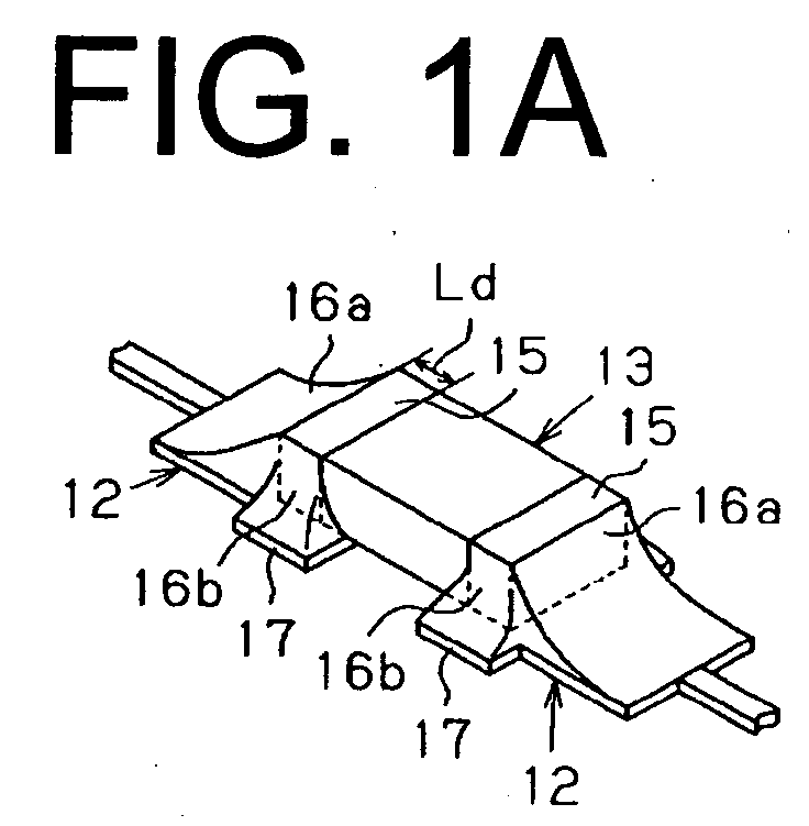
- FIG. 1A is a schematic perspective view showing a state where a chip component is mounted on a pair of lands according to a preferred embodiment of the present invention.
- FIG. 1B is a schematic plan view showing a relationship between the lands and the chip component according to the preferred embodiment of the present invention.
- FIG. 1C is a schematic perspective view showing the relationship between the chip component and the lands according to the preferred embodiment of the present invention.
- FIG. 1D is a schematic side view showing the state where the chip component is mounted on the lands according to the preferred embodiment of the present invention.
- FIG. 1A is a schematic perspective view showing a state where a chip component is mounted on a pair of lands according to a preferred embodiment of the present invention.
- FIG. 1B is a schematic plan view showing a relationship between the lands and the chip component according to the preferred embodiment of the present invention.
- FIG. 1C is a schematic perspective view showing the relationship between the chip component and the lands according to the preferred embodiment of the present invention.
- FIGS. 1A-1D and 2A-2C omit diagrammatic representations of solder resists for preventing solder from sticking on a wiring board other than the place to be soldered.
- a circuit board 11 (not shown in FIG. 1A) has formed on a surface thereof a pair of lands 12, on the pair of which a chip component 13 serving as a surface mounting electronic component is joined with solder 14.
- the chip component 13 is soldered on the lands 12 which form a conductor pattern formed on the surface of the circuit board 11 by a reflow soldering method. That is, the chip component 13 is mounted on the surface of the circuit board 11.
- the chip component 13 has a pair of electrodes 15 each of which has an end face 15a and a pair of side faces 15b.
- the lands 12 and the electrodes 15 are joined to each other respectively by solder fillets, each of which has a front fillet 16a and a pair of side fillets 16b.
- the front fillet 16a is formed in a position corresponding to the end face 15a of the electrode 15, and each side fillet 16b is formed in a position corresponding to the associated side face 15b of the electrode 15.
- the chip component 13 includes a ceramic condenser.
- the chip component 13 is formed in the shape of a rectangular parallelepiped, and has formed on both ends in a longitudinal direction thereof the electrodes 15 by means such as plating. That is, the chip component 13 has on a marginal portion thereof a plurality of electrodes 15, each of which is formed so as to at least cover the surface (the under surface) of the chip component 13 which faces the land 12, both side faces thereof and the end face thereof.
- the land 12 has a restricting portion 12a which restricts movement of the chip component 13 at the time of solder melting during surface mounting, and also has a protrusion 17 on each side of the corresponding electrode 15.
- the side fillet 16b is formed on each protrusion 17.
- the restricting portion 12a is formed by a corner at a boundary between a portion of the land 12, which has substantially the same width as the chip component 13, and the protrusion 17.
- a length L1 of the portion of the land 12 corresponding to the end face 15a of the electrode 15 in a direction perpendicular to the end face 15a is formed so as to be larger than maximum length Lm of the protrusion 17 in a direction perpendicular to the side face 15b of the electrode 15.
- the protrusion 17 is formed in a rectangular shape.
- the protrusion 17 preferably extends in a direction of the width of the land 12 by 10% of the width of the electrode 15 or above, and more preferably extends in the direction by 20% thereof or above. That is, the protrusion 17 is preferably formed so that the maximum length Lm thereof in the direction perpendicular to the side face 15b of the electrode 15 is 10% of the width of the electrode 15 or above, and is more preferably formed so that the maximum length Lm is 20% of the width of the electrode 15 or above. While the maximum length Lm is desirably lengthened in order to form the side fillet 16b, the lengthened maximum length Lm lowers mounting density for the chip component 13. Therefore, the maximum length Lm is suitably determined in accordance with a needed mounting density.
- a length L2 of the protrusion 17 along the side face 15b of the electrode 15 is formed so as to be larger than a length Ld of the side face 15b of the electrode 15. That is, the protrusion 17 protrudes from the inside end of the electrode 15 of the chip component 13 toward the opposed land 12 in a direction along the side face 15b of the electrode 15.
- the side fillet 16b is formed so as to cover the inside of both corners, in which generation of stress concentration is estimated to be particularly great, in the area between the under surface of the electrode 15 on the end of the chip component 13 and the land 12.
- the protrusion 17 protrudes from the end face 15a toward the counter side to the opposed land 12 in the direction along the side face 15b of the electrode 15. It is noted that the inside end of the electrode 15 of the chip component 13 means an end of the electrode 15 located on the middle side of the chip component 13.
- the land 12 has a portion 12b that protrudes from the inside end of the electrode 15 of the chip component 13 toward the middle of the chip component 13.
- the portion 12b is formed along the full length in the direction of the width of the electrode 15.
- an end of the protrusion 17 and a protruding end of the portion 12b are formed on the identical straight line.
- a temperature cycle test is conducted until 3000 cycles. A crack state is observed when every 1000 cycles finish.
- the temperature cycle test is also conducted for a comparative example in a case where the chip component 13 is mounted on a predetermined width of land 12 which is shown in FIG. 2A.
- the crack state is observed when every 1000 cycles finish.
- the sample of the practical example uses the dimensions shown in FIG. 1B, where the land width Lw is 1.7 mm, the maximum length Lm is 0.4 mm, the distance between lands Lh is 1.5 mm and the land length La is 2.5 mm. Meanwhile, two kinds of samples are prepared for comparative examples.
- One of the samples uses the dimensions shown in FIG. 2A, where the land width Lw is 1.7 mm, the land length La is 2.5 mm and the distance between lands Lh is 1.5 mm.
- the other sample uses the dimensions shown in FIG. 2A, where the land width Lw is 1.7 mm, the land length La is 2.5 mm and the distance between lands Lh is 1.7 mm.
- the chip component 13 has a width W of 1.6 mm and a distance between electrodes De that ranges from 2.0 to 2.2 mm, for both the practical example and the comparative examples.
- the number of samples is 24 for each of the practical example and the comparative examples.
- the temperature cycle test defines a period where the temperature is alternatively maintained between minus 40 degrees Celsius and 90 degrees Celsius as one cycle.
- no crack that causes rejection is observed in both of the practical example and the comparative examples.
- one crack that causes rejection is observed in the comparative example whose distance between lands Lh is 1.5 mm.
- the length of the observed crack is equal to or more than half of the thickness in a traveling direction of the crack.
- the number of rejected articles whose crack length is equal to or more than half of the thickness in the traveling direction of the crack is four.
- the number of rejected articles whose crack extends through the front fillet 16a in the traveling direction of the crack is one.
- the number of rejected articles whose crack length is equal to or more than half of the thickness in the traveling direction of the crack is two.
- the number of rejected articles whose crack extends through the front fillet 16a in the traveling direction of the crack is two.
- FIG. 2B shows a sectional view of the front fillet 16a on completion of 2000 cycles.
- the under surface of the electrode 15 of the chip component 13, which faces the land 12, and the land 12 have developed therebetween a crack 19.
- the reason the crack 19 is formed is considered that stress tends to concentrate on a relatively thin solder layer between the land 12 and the chip component 13 that adjacently face each other.
- the front fillet 16a has generated on a mountainside thereof a step 20 caused by a sliding phenomenon of metal which is considered to be caused by shear stress generated between the chip component 13 and the land 12.
- FIG. 2C shows a sectional view of the front fillet 16a on completion of 3000 cycles.
- the crack 19, which finally extends through the front fillet 16a changes as described in the comparative example whose distance between lands Lh is 1.7 mm.
- FIGS. 2B and 2C omit diagrammatic representations of hatching showing section.
- FIG. 3 shows a sectional view of the front fillet 16a of the practical example, in which no crack that causes rejection is observed, even on completion of 3000 cycles. This sectional view is based on the pictures observed by using a metallographic microscope.
- a black portion of the front fillet 16a is lead-rich ⁇ phase and the other portion thereof is tin-rich ⁇ phase (not shown in FIGS. 2B and 2C).
- lead and tin of the solder composition spread in both of the ⁇ phase and the ⁇ phase, and a state of grain growth is observed.
- FIG. 3 also omits diagrammatic representation of hatching showing section.
- the side fillet 16b is formed evenly in the position corresponding to the side face 15b of the electrode 15.
- the side fillet 16b exists so as to cover the inside of both corners, in which generation of a stress concentration is estimated to be particularly great, in the area between the under surface of the electrode 15 of the chip component 13 and the land 12. Therefore, stress concentration on the front fillet 16a is reduced, and the grain growth of the ⁇ phase and the ⁇ phase is restricted around the area between the under surface of the electrode 15 of the chip component 13, which faces the land 12, and the land 12. As a result, there considered that the development of crack is restrained.
- the present embodiment has the following advantageous effects.
- the present invention is not limited to the above-described embodiment, but may be embodied in the following manner.
- the shape of the protrusion 17 is not limited to the shape of the above-described embodiment. As shown in FIG. 4A, the protrusion 17 is formed in a semicircular shape whose diameter is longer than the length Ld of the side face 15b of the electrode 15. The portion 12b of the land 12 protruding toward the middle of the chip component 13 may be formed along the full length in the width direction of the electrode 15. Also, as shown in FIG 4B, the protrusion 17 is formed in the shape of a sector of a circle whose radius is equal to or less than the length Ld of the side face 15b of the electrode 15. In addition, the center of the protrusion 17 in the shape of the sector of the circle may be positioned so as to correspond to the inside end of the electrode 15.
- the portion 12b of the land 12 protruding toward the middle of the chip component 13 is formed in the shape of a quarter circle.
- a sector of a circle means a figure in a form that is surrounded by an arc and a straight line, inclusive of the figure in which the position of the center of the sector does not coincide with one end of the curvature radius of the arc.
- the value of its central angle is not limited to 180 degrees or below, but may exceed 180 degrees.
- the same temperature cycle test (each number of samples is 24) as in the preferred embodiment has been conducted for the samples such that the chip component 13 is mounted on two pairs of lands 12, respectively having the shapes shown in FIGS. 4A and 4B, however, such a crack that causes rejection was not observed on completion of 3000 cycles.
- the protrusion 17 does not correspond to the full length of the side face 15b of the electrode 15, in other words, the protrusion 17 is not formed near the end face 15a of the electrode 15, however, the temperature cycle test has brought a favorable result.
- This result means that the side fillet 16b formed between the side face 15b and the protrusion 17 does not necessarily need to be formed along the full length of the side face 15b.
- the similar effects (1) through (3) and (5) to those in the preferred embodiment are also obtained in a surface mounting structure that uses the lands 12 having shapes shown in FIGS. 4A and 4B.
- the restricting portion 12a has not only a corner the boundary between the portion of the land 12 whose width is substantially the same as that of the chip component 13, and the protrusion 17, but also a part of the portion of the land 12, of which width is substantially the same as that of the chip component 13.
- the land 12 has the restricting portions 12a that restrict the movement of the chip component 13 at the time of solder melting, and also has the protrusion 17 on each side of the corresponding electrode 15.
- the side fillet 16b is formed on each protrusion 17.
- the length L1 of the portion of the land 12 corresponding to the end face 15a of the electrode 15 in the direction perpendicular to the end face 15a is formed so as to be larger than the maximum length Lm of the protrusion 17 in the direction perpendicular to the side face 15b of the electrode 15.
- the shapes of the lands 12 shown in FIGS. 5A through 5D and 6A, 6B are also applicable. In the shapes of the lands 12 shown in FIGS.
- the widths of the protrusions 17 corresponding to the end faces 15a of the electrodes 15 are formed in a prescribed length.
- the protrusions 17 shown in FIGS. 5A through 5D have a trapezoidal shape, a shape formed by a curve and a straight line, an isosceles triangular shape and a right triangular shape, respectively.
- the restricting portion 12a is formed by the corner at the boundary between the portion of the land 12, which has substantially the same width as the chip component 13, and the protrusion 17.
- the lands 12 shown in FIGS. 6A and 6B are formed so that the widths of the portions of the lands 12 corresponding to the end faces 15a of the electrodes 15 decrease as distanced from the opposed lands 12 and that the visible outlines of the lands 12 are extended without being bent to form the visible outline in the direction of the width of the protrusion 17.
- the restricting portions 12a of each land are positioned so that the distance between the visible outlines in the width direction of the protrusions 17 (the distance between the intersection points of a straight line parallel to the width direction of the chip component 13 with both of the visible outlines) is substantially equal to the width of the chip component 13.
- the expression “substantially equal to the width of the chip component 13” means “equal to the width of the chip component 13 or above in an allowable error range of the positional deviation during the surface mounting”.
- the protrusion 17 is located outside the straight line (not shown) that passes the restricting portion 12a and is parallel to a center line Lc of the land 12.
- the land 12 may be formed so that the width of the portion of the land 12 corresponding to the end face 15a of the electrode 15 decrease as distanced from the end face 15a in a case where the visible outlines of the land 12 are bent in the restricting portions 12a.
- the land 12 does not necessarily need to have the portion 12b that protrudes from the inside end of the electrode 15 of the chip component 13 toward the middle of the chip component 13.
- the portion 12b that protrudes from the inside end of the electrode 15 of the chip component 13 toward the middle of the chip component 13 may be eliminated from the land 12.
- the land 12b does not need to be continuously formed with the protrusion 17, but may be formed separately from the protrusion 17.
- the protrusion 17 needs to be formed in size such that the side fillet 16b is formed at least between the protrusion 17 and the side face 15b of the electrode 15. That is, the side fillet 16b does not necessarily need to be formed along the full length of the side face 15b.
- the protrusion 17 does not necessarily need to have a portion that protrudes from the inside end of the electrode 15 toward the opposed land 12.
- each land 12 has a symmetrical shape with respect to the center line Lc
- the land 12 does not need to have the symmetrical shape with respect to the center line Lc.
- the paired protrusions 17 of the land 12 may have different shapes from each other. However, if the land 12 has a symmetrical shape, self-alignment of the chip component 13 at the time of solder melting during the surface mounting is smoothly achieved.
- the method is not restricted to form the land 12 in the desired shape by etching or plating a conductor pattern of the land 12.
- solder resist machining may be performed by forming an opening of the land in a desired shape on a solid conductor pattern of which width is larger than that of the land 12.
- the chip component (electronic component) 13 needs only to have on a marginal portion thereof a plurality of electrodes, each of which is formed so as to cover at least the under surface of the chip component 13, which faces the land 12, both side faces of the chip component 13 and the end face of the chip component 13.
- the chip component 13 is not necessarily restricted to a shape such that a pair of electrodes is formed on both ends of a rectangular parallelepiped, and may have three or more electrodes.
- the chip component (electronic component) 13 needs only to be formed so that each electrode covers at least the under surface of the chip component 13, which faces the land 12, both side faces of the chip component 13 and the end face of the chip component 13.
- the chip component 13 is not restricted to the ceramic condenser, but may be a resistance or a diode.
- the resistance in the shape of a chip does not generally have on both side faces thereof a pair of electrodes.
- the distance between the adjacent lands 12 needs to be distanced in order to ensure an insulation distance compared to the case where the lands 12 do not have the protrusions 17.
- the lands 12 are arranged so as to arrange the chip components 13 in zigzag, the chip components 13 are mounted in a state that the distance between the adjacent chip components 13 is substantially the same for the case where the lands 12 do not have the protrusions 17.
- the values such as the land width Lw, the maximum length Lm, the distance between lands Lh and the land length La are modified in accordance with the size.
- solder for use in the surface mounting is not restricted to the alloy of lead and tin, but may be so-called a leadfree solder which is made of an alloy of tin as a main component and metal other than lead.
- a surface mounting structure for a surface mounting electronic component includes an electronic component, a circuit board and a solder fillet.
- the electronic component has on a marginal portion thereof a plurality of electrodes, each of which is formed so as to cover at least an under surface, both side faces and an end face of the electronic component.
- the circuit board has a set of lands, on which the electrodes of the electronic component are joined by soldering. Each land corresponds to one of the electrodes and has a restricting portion, which restricts movement of the electronic component at the time of solder melting during surface mounting, and also has a protrusion on each side of the corresponding electrode.
- the solder fillet is formed at least on each protrusion so as to correspond to both side faces of the corresponding electrode.
Landscapes
- Engineering & Computer Science (AREA)
- Microelectronics & Electronic Packaging (AREA)
- Manufacturing & Machinery (AREA)
- Electric Connection Of Electric Components To Printed Circuits (AREA)
Abstract


Description
- The present invention relates to a surface mounting structure for a surface mounting electronic component, and more particularly to a surface mounting structure for a surface mounting electronic component wherein the surface mounting electronic component is joined on a land of a circuit board by soldering.
- Since a solder joint has an excellent advantage in that a bonding operation is relatively easy, that bonding strength is reliably firm and that its cost is low, the solder joint has been used for various purposes in mounting an electronic component.
- Meanwhile, in order to mount the electronic component in high density for miniaturization of an electronic device, the mainstream of a mounting structure for the electronic component is changing from an insertion mount that uses a lead component to a surface mounting that uses a surface mounting electronic component (chip component).
- In a case where a surface mounting electronic component such as a ceramic condenser is mounted, as shown in FIG. 7A, a
chip component 51 in the shape of a rectangular parallelepiped has formed on both ends thereof anelectrode 52. In a state where acircuit board 53 has formed on the surface thereof a pair oflands 54, on each of which acream solder 55 is printed, eachelectrode 52 of thechip component 51 is mounted on thecream solder 55 of thecorresponding land 54. Subsequently, thecream solder 55 is melted (reflowed) in a reflow furnace by heat, thereby mounting thechip component 51 on thecircuit board 53 by solder joints. - In a case where a service condition for the electronic device has temperature changes in a narrow range, normal solder joints are acceptable. However, a service condition for an electronic device for automobile use requires resistance to a temperature change between below zero and a few dozen degrees Celsius. That is, reliability in hot and cold environments and reliability in temperature cycling between the hot and cold environments are required.
- In general, materials expand due to temperature rise and shrink due to temperature fall, and those degrees (coefficient of liner expansion) differ among the materials. Since the circuit board (land) side and the electronic component of a solder mounting portion for the electronic component have the different coefficients, thermal stress generates in a solder joining area between the circuit board side and the electronic component in accordance with temperature variations. As the generation of the thermal stress is repeated for an extended period, Lead(Pb)-rich α phase and tin(Sn)-rich β phase of solder composition spread thereby causing grain growth. The boundary between the crystal grains of the α phase and the β phase is fragile. Also, in a case where the land is made of copper (Cu), a Cu-Sn alloy layer is generated, however, this alloy layer is still hard and fragile. Cracks are generated mainly along such a fragile crystal grain boundary or an alloy layer. When the crack extends, the solder joining area may be broken thereby causing breakdown.
- In order that breakage of the electronic component and deterioration of electrical characteristics are prevented, even if the thermal history such as heating or cooling increases during use of the electronic component mounted on the circuit board, a surface mounting structure for an electronic component is proposed such that the line width of the wiring pattern (land), the width of the electronic component, the distance between the lands, and the distance between electrodes of terminals meet a specific relation among them.
- Japanese Unexamined Patent Publication No. 11-17308 discloses the surface mounting structure for an electronic component. As shown in FIG. 8, an
electronic component 57 is joined on the pair oflands 54 formed on thecircuit board 53 bysolder 56. The surface mounting structure meets the relations 1.0≤Wh/Ws≤1.2 and 0.8≤Dh/De<1.0 where the line width of theland 54 is Wh, the width of the electronic component is Ws, the distance between thelands 54 is Dh, and the distance between the electrodes of the terminals is De. In the surface mounting structure for the electronic component, a heat shock test is conducted until 2000 cycles. The heat shock test defines a period where the surface mounting structure is alternatively immersed in solutions of minus 40 degrees Celsius and 130 degrees Celsius as one cycle. In the surface mounting structure for the electronic component which meets the relations, the number of electronic components which have been cracked on completion of 2000 cycles does not exceed 10% of the initial number (50) of electronic components, thereby being regarded as being sufficiently reliable. - The inventors of the present application have cut a specimen which was used in a temperature cycle test and have observed its cross section. As a result, as shown in FIG. 7B, a
solder fillet 58 had acrack 59 first between the under surface of theelectrode 52 and theland 54, and then thecrack 59 extended slowly and finally extended through thesolder fillet 58. It is noted that FIG. 7B shows one side of thechip component 51. The expression "thecrack 59 extends through thesolder fillet 58" means that the crack extends in a sheet so as to divide the solder joining area into a land side and an electrode side, thereby preventing electric continuity between the electrode and the land. - The
chip component 51 and theland 54, which have different coefficients of liner expansion, tend to cause a stress concentration on the area between the under surface of eachelectrode 52 of thechip component 51 and theland 54 where thechip component 51 and theland 54 lie next to each other at the closest position. It is estimated that the stress concentration is particularly great at the inside of both corners in the area between the under surface of eachelectrode 52 of thechip component 51 and theland 54. - The inventors of the present application have provided the solder fillet formed between the electrode of the electronic component and the land, not only in the position corresponding to the end face of the electrode, but also in the positions corresponding to both side faces of the electrode, thereby reducing the stress concentration on the inside of both corners. The idea of the inventors has been proved by performing the temperature cycle test of 3000 cycles. If the solder fillet is provided only in the positions corresponding to both side faces of the electrode, the land width only has to be increased compared to the width of electronic component. However, in a case where the land width is merely increased, when the solder joint is achieved by mounting the electronic component on the cream solder printed on the land and melting the solder by heat, the electronic component deviates from its desirable position.
- While Japanese Unexamined Patent Publication No. 11-17308 discloses that the line width Wh of the
land 54 is equal to or more than the width Ws of the electronic component and that the line width Wh of theland 54 is equal to or less than 120% of the width Ws of the electronic component, its object is directed to breakage of theelectronic component 57 and prevention of deterioration of electrical characteristics without particularly referring to the prevention of the crack generation of the solder fillet. As to the deviation of the position of the electronic component, while the cited reference discloses that the thickness of the solder existing between the electrode of theelectronic component 57 and the surface of theland 54 preferably ranges between 90 µm and 500 µm inclusive of 90 µm and 500 µm, the reference does not disclose any relation between the width of theland 54 and the deviation of the position. - The present invention is directed to a surface mounting structure for a surface mounting electronic component that improves a crack-resistance to a temperature cycle while maintaining assembly operation similar to the prior art.
- The present invention provides the following features. A surface mounting structure for a surface mounting electronic component includes an electronic component, a circuit board and a solder fillet. The electronic component has on a marginal portion thereof a plurality of electrodes, each of which is formed so as to cover at least an under surface, both side faces and an end face of the electronic component. The circuit board has a set of lands, on which the electrodes of the electronic component are joined by soldering. Each land corresponds to one of the electrodes and has a restricting portion, which restricts movement of the electronic component at the time of solder melting during surface mounting, and also has a protrusion on each side of the corresponding electrode. The solder fillet is formed at least on each protrusion so as to correspond to both side faces of the corresponding electrode.
- Other aspects and advantages of the invention will become apparent from the following description, taken in conjunction with the accompanying drawings, illustrating by way of example the principles of the invention.
- The features of the present invention that are believed to be novel are set forth with particularity in the appended claims. The invention, together with objects and advantages thereof, may best be understood by reference to the following description of the presently preferred embodiments, together with the accompanying drawings, in which:
- FIG. 1A is a schematic perspective view showing a state where a chip component is mounted on a pair of lands according to a preferred embodiment of the present invention;
- FIG. 1B is a schematic plan view showing a relationship between the lands and the chip component according to the preferred embodiment of the present invention;
- FIG. 1C is a schematic perspective view showing the relationship between the chip component and the lands according to the preferred embodiment of the present invention;
- FIG. 1D is a schematic side view showing the state where the chip component is mounted on the lands according to the preferred embodiment of the present invention;
- FIG. 2A is a schematic plan view showing a relationship between a chip component and a pair of lands of a comparative example;
- FIG. 2B is a schematic sectional view showing a state of the comparative example after a temperature cycle test is conducted;
- FIG. 2C is a schematic sectional view showing a state of the comparative example after the temperature cycle test is conducted;
- FIG. 3 is a schematic sectional view showing a state of a practical example after the temperature cycle test is conducted;
- FIG. 4A is a schematic plan view showing a relationship between a pair of lands and a chip component according to another preferred embodiment of the present invention;
- FIG 4B is a schematic plan view showing a relationship between a pair of lands and a chip component according to another preferred embodiment of the present invention;
- FIG. 5A is a schematic plan view showing a relationship between a pair of lands and a chip component according to another preferred embodiment of the present invention;
- FIG. 5B is a schematic plan view showing a relationship between a pair of lands and a chip component according to another preferred embodiment of the present invention;
- FIG. 5C is a schematic plan view showing a relationship between a pair of lands and a chip component according to another preferred embodiment of the present invention;
- FIG. 5D is a schematic plan view showing a relationship between a pair of lands and a chip component according to another preferred embodiment of the present invention;
- FIG. 6A is a schematic plan view showing a relationship between a pair of lands and a chip component according to another preferred embodiment of the present invention;
- FIG. 6B is a schematic plan view showing a relationship between a pair of lands and a chip component according to another preferred embodiment of the present invention;
- FIG. 7A is a schematic perspective view showing a prior art relationship between a pair of lands and a chip component;
- FIG. 7B is a schematic side view showing a prior art crack; and
- FIG. 8 is a schematic perspective view showing a prior art relationship between a pair of lands and a chip component.
-
- A preferred embodiment of the present invention will now be described with reference to FIGS. 1A-1 D, 2A-2C and 3. FIG. 1A is a schematic perspective view showing a state where a chip component is mounted on a pair of lands according to a preferred embodiment of the present invention. FIG. 1B is a schematic plan view showing a relationship between the lands and the chip component according to the preferred embodiment of the present invention. FIG. 1C is a schematic perspective view showing the relationship between the chip component and the lands according to the preferred embodiment of the present invention. FIG. 1D is a schematic side view showing the state where the chip component is mounted on the lands according to the preferred embodiment of the present invention. FIG. 2A is a schematic plan view showing a relationship between a chip component and a pair of lands of a comparative example. FIG. 2B is a schematic sectional view showing a state of the comparative example after a temperature cycle test is conducted. FIG. 2C is a schematic sectional view showing a state of the comparative example after the temperature cycle test is conducted. FIG. 3 is a schematic sectional view showing a state of a practical example after the temperature cycle test is conducted. It is noted that FIGS. 1A-1D and 2A-2C omit diagrammatic representations of solder resists for preventing solder from sticking on a wiring board other than the place to be soldered.
- As shown in FIGS. 1A and 1D, a circuit board 11 (not shown in FIG. 1A) has formed on a surface thereof a pair of
lands 12, on the pair of which achip component 13 serving as a surface mounting electronic component is joined withsolder 14. Thechip component 13 is soldered on thelands 12 which form a conductor pattern formed on the surface of thecircuit board 11 by a reflow soldering method. That is, thechip component 13 is mounted on the surface of thecircuit board 11. Thechip component 13 has a pair ofelectrodes 15 each of which has anend face 15a and a pair of side faces 15b. Thelands 12 and theelectrodes 15 are joined to each other respectively by solder fillets, each of which has afront fillet 16a and a pair ofside fillets 16b. Thefront fillet 16a is formed in a position corresponding to theend face 15a of theelectrode 15, and eachside fillet 16b is formed in a position corresponding to the associatedside face 15b of theelectrode 15. Thechip component 13 includes a ceramic condenser. - In the present embodiment, the
chip component 13 is formed in the shape of a rectangular parallelepiped, and has formed on both ends in a longitudinal direction thereof theelectrodes 15 by means such as plating. That is, thechip component 13 has on a marginal portion thereof a plurality ofelectrodes 15, each of which is formed so as to at least cover the surface (the under surface) of thechip component 13 which faces theland 12, both side faces thereof and the end face thereof. - As shown in FIG. 1B, the
land 12 has a restrictingportion 12a which restricts movement of thechip component 13 at the time of solder melting during surface mounting, and also has aprotrusion 17 on each side of the correspondingelectrode 15. Theside fillet 16b is formed on eachprotrusion 17. In the present embodiment, the restrictingportion 12a is formed by a corner at a boundary between a portion of theland 12, which has substantially the same width as thechip component 13, and theprotrusion 17. A length L1 of the portion of theland 12 corresponding to theend face 15a of theelectrode 15 in a direction perpendicular to theend face 15a is formed so as to be larger than maximum length Lm of theprotrusion 17 in a direction perpendicular to theside face 15b of theelectrode 15. In the present embodiment, theprotrusion 17 is formed in a rectangular shape. - The
protrusion 17 preferably extends in a direction of the width of theland 12 by 10% of the width of theelectrode 15 or above, and more preferably extends in the direction by 20% thereof or above. That is, theprotrusion 17 is preferably formed so that the maximum length Lm thereof in the direction perpendicular to theside face 15b of theelectrode 15 is 10% of the width of theelectrode 15 or above, and is more preferably formed so that the maximum length Lm is 20% of the width of theelectrode 15 or above. While the maximum length Lm is desirably lengthened in order to form theside fillet 16b, the lengthened maximum length Lm lowers mounting density for thechip component 13. Therefore, the maximum length Lm is suitably determined in accordance with a needed mounting density. - A length L2 of the
protrusion 17 along theside face 15b of theelectrode 15 is formed so as to be larger than a length Ld of theside face 15b of theelectrode 15. That is, theprotrusion 17 protrudes from the inside end of theelectrode 15 of thechip component 13 toward theopposed land 12 in a direction along theside face 15b of theelectrode 15. Theside fillet 16b is formed so as to cover the inside of both corners, in which generation of stress concentration is estimated to be particularly great, in the area between the under surface of theelectrode 15 on the end of thechip component 13 and theland 12. In the present embodiment, theprotrusion 17 protrudes from theend face 15a toward the counter side to the opposedland 12 in the direction along theside face 15b of theelectrode 15. It is noted that the inside end of theelectrode 15 of thechip component 13 means an end of theelectrode 15 located on the middle side of thechip component 13. - The
land 12 has aportion 12b that protrudes from the inside end of theelectrode 15 of thechip component 13 toward the middle of thechip component 13. Theportion 12b is formed along the full length in the direction of the width of theelectrode 15. In the present embodiment, an end of theprotrusion 17 and a protruding end of theportion 12b are formed on the identical straight line. - In a case where the
chip component 13 is mounted on the surface of theland 12, in a state where the surface of thecircuit board 11 is covered with solder resist except for a portion necessary for soldering, as shown in FIG. 1C,cream solder 18 is printed on theland 12. Theelectrodes 15 of thechip component 13 are mounted on thecream solder 18. Subsequently, thecircuit board 11 is entered into a reflow furnace in which thecream solder 18 is melted (reflowed) by heat, thereby mounting thechip component 13 on thecircuit board 11 by solder joints. Since theland 12 has the restrictingportion 12a, self-alignment of thechip component 13 is achieved at the time of solder melting. Consequently, thechip component 13 is mounted on theland 12 and is prevented from deviating from its suitable position. - In order to check the durability to the temperature cycle of the above-mentioned surface mounting structure, a temperature cycle test is conducted until 3000 cycles. A crack state is observed when every 1000 cycles finish. The temperature cycle test is also conducted for a comparative example in a case where the
chip component 13 is mounted on a predetermined width ofland 12 which is shown in FIG. 2A. In a similar manner to the above-mentioned surface mounting structure, the crack state is observed when every 1000 cycles finish. Specifically, in a state where a sample which has passed a predetermined cycle is molded by a resin mold and thefront fillet 16a of the molded sample is cut by a plane that is parallel to the longitudinal direction of thechip component 13 and is perpendicular to theland 12, the crack state in the cut surface is observed. - The sample of the practical example uses the dimensions shown in FIG. 1B, where the land width Lw is 1.7 mm, the maximum length Lm is 0.4 mm, the distance between lands Lh is 1.5 mm and the land length La is 2.5 mm. Meanwhile, two kinds of samples are prepared for comparative examples. One of the samples uses the dimensions shown in FIG. 2A, where the land width Lw is 1.7 mm, the land length La is 2.5 mm and the distance between lands Lh is 1.5 mm. The other sample uses the dimensions shown in FIG. 2A, where the land width Lw is 1.7 mm, the land length La is 2.5 mm and the distance between lands Lh is 1.7 mm. The
chip component 13 has a width W of 1.6 mm and a distance between electrodes De that ranges from 2.0 to 2.2 mm, for both the practical example and the comparative examples. The number of samples is 24 for each of the practical example and the comparative examples. - The temperature cycle test defines a period where the temperature is alternatively maintained between minus 40 degrees Celsius and 90 degrees Celsius as one cycle. As a test result, on completion of 1000 cycles no crack that causes rejection is observed in both of the practical example and the comparative examples. On completion of 2000 cycles, while no crack that causes rejection is observed in the practical example, one crack that causes rejection is observed in the comparative example whose distance between lands Lh is 1.5 mm. The length of the observed crack is equal to or more than half of the thickness in a traveling direction of the crack.
- On completion of 3000 cycles, while no crack that causes rejection is observed in the practical example, cracks that cause rejection are observed in both of the comparative examples. In the comparative example whose distance between lands Lh is 1.7 mm, the number of rejected articles whose crack length is equal to or more than half of the thickness in the traveling direction of the crack is four. In addition, the number of rejected articles whose crack extends through the
front fillet 16a in the traveling direction of the crack is one. Also, in the comparative example whose distance between lands Lh is 1.5 mm, the number of rejected articles whose crack length is equal to or more than half of the thickness in the traveling direction of the crack is two. In addition, the number of rejected articles whose crack extends through thefront fillet 16a in the traveling direction of the crack is two. - In the comparative example whose distance between lands Lh is 1.7 mm, the development of a typical crack will be described. FIG. 2B shows a sectional view of the
front fillet 16a on completion of 2000 cycles. First, the under surface of theelectrode 15 of thechip component 13, which faces theland 12, and theland 12 have developed therebetween acrack 19. The reason thecrack 19 is formed is considered that stress tends to concentrate on a relatively thin solder layer between theland 12 and thechip component 13 that adjacently face each other. Thefront fillet 16a has generated on a mountainside thereof astep 20 caused by a sliding phenomenon of metal which is considered to be caused by shear stress generated between thechip component 13 and theland 12. Thereafter, thecrack 19 is developed toward thestep 20, and finally extends through thefront fillet 16a. FIG. 2C shows a sectional view of thefront fillet 16a on completion of 3000 cycles. In the comparative example whose distance between lands Lh is 1.5 mm, thecrack 19, which finally extends through thefront fillet 16a, changes as described in the comparative example whose distance between lands Lh is 1.7 mm. It is noted that FIGS. 2B and 2C omit diagrammatic representations of hatching showing section. - FIG. 3 shows a sectional view of the
front fillet 16a of the practical example, in which no crack that causes rejection is observed, even on completion of 3000 cycles. This sectional view is based on the pictures observed by using a metallographic microscope. In partial enlarged views of FIG. 3, a black portion of thefront fillet 16a is lead-rich α phase and the other portion thereof is tin-rich β phase (not shown in FIGS. 2B and 2C). Around the area between the under surface of theelectrode 15 of thechip component 13, which faces theland 12, and theland 12, which is first cracked, lead and tin of the solder composition spread in both of the α phase and the β phase, and a state of grain growth is observed. However, in the mountainside of thefront fillet 16a, which causes thestep 20 in the comparative examples, the aforementioned grain growth is hardly observed, and a fine crystalline state is observed in both of the α phase and the β phase. In addition, the generation of thestep 20 is relatively few. It is noted that FIG. 3 also omits diagrammatic representation of hatching showing section. - In the practical example, the
side fillet 16b is formed evenly in the position corresponding to theside face 15b of theelectrode 15. Theside fillet 16b exists so as to cover the inside of both corners, in which generation of a stress concentration is estimated to be particularly great, in the area between the under surface of theelectrode 15 of thechip component 13 and theland 12. Therefore, stress concentration on thefront fillet 16a is reduced, and the grain growth of the α phase and the β phase is restricted around the area between the under surface of theelectrode 15 of thechip component 13, which faces theland 12, and theland 12. As a result, there considered that the development of crack is restrained. - The present embodiment has the following advantageous effects.
- (1) In a mounting structure of the
chip component 13 which is mounted on theland 12 of thecircuit board 11 with thesolder 14, theland 12 has the restrictingportion 12a which restricts movement of thechip component 13 at the time of solder melting during the surface mounting, and also has theprotrusion 17 on each side of the correspondingelectrode 15. Theside fillet 16b is formed on eachprotrusion 17. Therefore, even if the width Lw of theland 12 is widened by the length of "Lm x 2" that is needed to suitably form theside fillet 16b on each side of theelectrode 15, in a case where the solder joint is achieved by mounting thechip component 13 on thecream solder 18 printed on theland 12 and melting the solder by heat, the deviation of the position of thechip component 13 from the suitable position is prevented, thus improving crack resistance to the temperature cycle while maintaining assembly operating performance as is conventionally done. For example, in the temperature cycle test, the crack resistance to the surface mounting structure of the present embodiment is 3000 cycles or above. - (2) The
protrusion 17 protrudes from the inside end of theelectrode 15 of thechip component 13 toward theopposed land 12 in the direction along theside face 15b of theelectrode 15. Therefore, theside fillet 16b exists so as to cover the inside of both corners, in which generation of a stress concentration is estimated to be particularly great. As a result, the crack resistance to the temperature cycle is further improved. - (3) The
protrusion 17 protrudes in the direction of the width of theland 12 by 10% of the width of theelectrode 15 or above. Therefore, in addition to thefront fillet 16a, a suitably-sized side fillet 16b which joins theland 12 and theelectrode 15 together is formed in the position corresponding to theside face 15b of theelectrode 15. - (4) The
land 12 has theportion 12b that protrudes from the inside end of theelectrode 15 of thechip component 13 toward the middle of thechip component 13. Therefore, thermal stress generated between the under surface of theelectrode 15, which faces theland 12, and theland 12 is further reduced. - (5) The
protrusion 17 is formed in a rectangular shape, and the length L2 of theprotrusion 17 in the direction along theside face 15b of theelectrode 15 is formed so as to be larger than the length Ld of theside face 15b of theelectrode 15. Theportion 12b of theland 12 protruding toward the middle of thechip component 13 is formed along the full length in the width direction of theelectrode 15. Therefore, compared to a case where theprotrusion 17 is formed in a semicircular shape (in the shape of a sector of a circle), in a case where the maximum length Lm of therectangular protrusion 17 in a direction perpendicular to theside face 15b of theelectrode 15 is the same size as that of thesemicircular protrusion 17, the area of theprotrusion 17 is increased, thereby easily ensuring that a suitable amount of solder forms theside fillet 16b on theside face 15b of theelectrode 15. - (6) Since the
protrusions 17 are symmetrically formed relative to theland 12, compared to a case where theprotrusions 17 are asymmetrically formed relative to theland 12, thechip component 13 tends to be mounted accurately in a prescribed position with solder. -
- The present invention is not limited to the above-described embodiment, but may be embodied in the following manner.
- The shape of the
protrusion 17 is not limited to the shape of the above-described embodiment. As shown in FIG. 4A, theprotrusion 17 is formed in a semicircular shape whose diameter is longer than the length Ld of theside face 15b of theelectrode 15. Theportion 12b of theland 12 protruding toward the middle of thechip component 13 may be formed along the full length in the width direction of theelectrode 15. Also, as shown in FIG 4B, theprotrusion 17 is formed in the shape of a sector of a circle whose radius is equal to or less than the length Ld of theside face 15b of theelectrode 15. In addition, the center of theprotrusion 17 in the shape of the sector of the circle may be positioned so as to correspond to the inside end of theelectrode 15. In this case, theportion 12b of theland 12 protruding toward the middle of thechip component 13 is formed in the shape of a quarter circle. It is noted that the expression "a sector of a circle" means a figure in a form that is surrounded by an arc and a straight line, inclusive of the figure in which the position of the center of the sector does not coincide with one end of the curvature radius of the arc. In addition, the value of its central angle is not limited to 180 degrees or below, but may exceed 180 degrees. The same temperature cycle test (each number of samples is 24) as in the preferred embodiment has been conducted for the samples such that thechip component 13 is mounted on two pairs oflands 12, respectively having the shapes shown in FIGS. 4A and 4B, however, such a crack that causes rejection was not observed on completion of 3000 cycles. - In the
land 12 shown in FIG. 4B, theprotrusion 17 does not correspond to the full length of theside face 15b of theelectrode 15, in other words, theprotrusion 17 is not formed near theend face 15a of theelectrode 15, however, the temperature cycle test has brought a favorable result. This result means that theside fillet 16b formed between theside face 15b and theprotrusion 17 does not necessarily need to be formed along the full length of theside face 15b. The similar effects (1) through (3) and (5) to those in the preferred embodiment are also obtained in a surface mounting structure that uses thelands 12 having shapes shown in FIGS. 4A and 4B. In theland 12 shown in FIG. 4B, the restrictingportion 12a has not only a corner the boundary between the portion of theland 12 whose width is substantially the same as that of thechip component 13, and theprotrusion 17, but also a part of the portion of theland 12, of which width is substantially the same as that of thechip component 13. As a result, the self-alignment at the time of solder melting during the surface mounting is favorably performed. - The
land 12 has the restrictingportions 12a that restrict the movement of thechip component 13 at the time of solder melting, and also has theprotrusion 17 on each side of the correspondingelectrode 15. Theside fillet 16b is formed on eachprotrusion 17. Preferably, the length L1 of the portion of theland 12 corresponding to theend face 15a of theelectrode 15 in the direction perpendicular to theend face 15a is formed so as to be larger than the maximum length Lm of theprotrusion 17 in the direction perpendicular to theside face 15b of theelectrode 15. The shapes of thelands 12 shown in FIGS. 5A through 5D and 6A, 6B are also applicable. In the shapes of thelands 12 shown in FIGS. 5A through 5D, while the shapes of theprotrusions 17 are different from each other, the widths of theprotrusions 17 corresponding to the end faces 15a of theelectrodes 15 are formed in a prescribed length. It is noted that theprotrusions 17 shown in FIGS. 5A through 5D have a trapezoidal shape, a shape formed by a curve and a straight line, an isosceles triangular shape and a right triangular shape, respectively. In this case, the restrictingportion 12a is formed by the corner at the boundary between the portion of theland 12, which has substantially the same width as thechip component 13, and theprotrusion 17. - Meanwhile, the
lands 12 shown in FIGS. 6A and 6B are formed so that the widths of the portions of thelands 12 corresponding to the end faces 15a of theelectrodes 15 decrease as distanced from the opposed lands 12 and that the visible outlines of thelands 12 are extended without being bent to form the visible outline in the direction of the width of theprotrusion 17. In thelands 12 shown in FIGS. 6A and 6B, the restrictingportions 12a of each land are positioned so that the distance between the visible outlines in the width direction of the protrusions 17 (the distance between the intersection points of a straight line parallel to the width direction of thechip component 13 with both of the visible outlines) is substantially equal to the width of thechip component 13. The expression "substantially equal to the width of thechip component 13" means "equal to the width of thechip component 13 or above in an allowable error range of the positional deviation during the surface mounting". Theprotrusion 17 is located outside the straight line (not shown) that passes the restrictingportion 12a and is parallel to a center line Lc of theland 12. - The
land 12 may be formed so that the width of the portion of theland 12 corresponding to theend face 15a of theelectrode 15 decrease as distanced from theend face 15a in a case where the visible outlines of theland 12 are bent in the restrictingportions 12a. - The
land 12 does not necessarily need to have theportion 12b that protrudes from the inside end of theelectrode 15 of thechip component 13 toward the middle of thechip component 13. In the above-mentioned embodiments, theportion 12b that protrudes from the inside end of theelectrode 15 of thechip component 13 toward the middle of thechip component 13 may be eliminated from theland 12. Theland 12b does not need to be continuously formed with theprotrusion 17, but may be formed separately from theprotrusion 17. - The
protrusion 17 needs to be formed in size such that theside fillet 16b is formed at least between theprotrusion 17 and theside face 15b of theelectrode 15. That is, theside fillet 16b does not necessarily need to be formed along the full length of theside face 15b. Theprotrusion 17 does not necessarily need to have a portion that protrudes from the inside end of theelectrode 15 toward theopposed land 12. - Although in the above-mentioned embodiments each
land 12 has a symmetrical shape with respect to the center line Lc, theland 12 does not need to have the symmetrical shape with respect to the center line Lc. The pairedprotrusions 17 of theland 12 may have different shapes from each other. However, if theland 12 has a symmetrical shape, self-alignment of thechip component 13 at the time of solder melting during the surface mounting is smoothly achieved. - As to a method of forming the
land 12 in a desired shape, the method is not restricted to form theland 12 in the desired shape by etching or plating a conductor pattern of theland 12. For example, solder resist machining may be performed by forming an opening of the land in a desired shape on a solid conductor pattern of which width is larger than that of theland 12. - The chip component (electronic component) 13 needs only to have on a marginal portion thereof a plurality of electrodes, each of which is formed so as to cover at least the under surface of the
chip component 13, which faces theland 12, both side faces of thechip component 13 and the end face of thechip component 13. Thechip component 13 is not necessarily restricted to a shape such that a pair of electrodes is formed on both ends of a rectangular parallelepiped, and may have three or more electrodes. - The chip component (electronic component) 13 needs only to be formed so that each electrode covers at least the under surface of the
chip component 13, which faces theland 12, both side faces of thechip component 13 and the end face of thechip component 13. Thechip component 13 is not restricted to the ceramic condenser, but may be a resistance or a diode. The resistance in the shape of a chip does not generally have on both side faces thereof a pair of electrodes. - In a case where a plurality of
chip components 13 are mounted by using thelands 12 having theprotrusions 17, if thechip components 13 are arranged parallel to each other and thelands 12 of theadjacent chip components 13 are also adjacently juxtaposed, the distance between theadjacent lands 12 needs to be distanced in order to ensure an insulation distance compared to the case where thelands 12 do not have theprotrusions 17. However, if thelands 12 are arranged so as to arrange thechip components 13 in zigzag, thechip components 13 are mounted in a state that the distance between theadjacent chip components 13 is substantially the same for the case where thelands 12 do not have theprotrusions 17. - If a size of the
chip component 13 is varied, the values such as the land width Lw, the maximum length Lm, the distance between lands Lh and the land length La are modified in accordance with the size. - The solder for use in the surface mounting is not restricted to the alloy of lead and tin, but may be so-called a leadfree solder which is made of an alloy of tin as a main component and metal other than lead.
- Therefore, the present examples and embodiments are to be considered as illustrative and not restrictive and the invention is not to be limited to the details given herein but may be modified.
- A surface mounting structure for a surface mounting electronic component includes an electronic component, a circuit board and a solder fillet. The electronic component has on a marginal portion thereof a plurality of electrodes, each of which is formed so as to cover at least an under surface, both side faces and an end face of the electronic component. The circuit board has a set of lands, on which the electrodes of the electronic component are joined by soldering. Each land corresponds to one of the electrodes and has a restricting portion, which restricts movement of the electronic component at the time of solder melting during surface mounting, and also has a protrusion on each side of the corresponding electrode. The solder fillet is formed at least on each protrusion so as to correspond to both side faces of the corresponding electrode.
Claims (9)
- A surface mounting structure for a surface mounting electronic component, characterized in that an electronic component has on a marginal portion thereof a plurality of electrodes, each of which is formed so as to cover at least an under surface, both side faces and an end face of the electronic component, in that a circuit board has a set of lands, on which the electrodes of the electronic component are joined by soldering, in that each land corresponding to one of the electrodes has a restricting portion, which restricts movement of the electronic component at the time of solder melting during surface mounting, and also has a protrusion on each side of the corresponding electrode, and in that a solder fillet is formed at least on each protrusion so as to correspond to both side faces of the corresponding electrode.
- The surface mounting structure according to claim 1, wherein each protrusion of one of the lands is formed so as to protrude from an inside end of the corresponding electrode toward an opposed land in a direction along a side face of the corresponding electrode.
- The surface mounting structure according to claim 1 or 2, wherein each protrusion of one of the lands is formed so as to protrude in a width direction of that land by 10 % of a width of the corresponding electrode or above.
- The surface mounting structure according to any one of claims 1 through 3, wherein each land has a portion that protrudes from an inside end of the corresponding electrode toward a middle of the electronic component.
- The surface mounting structure according to any one of claims 1 through 4, wherein each protrusion of one of the lands is formed in the shape of a sector of a circle whose radius is equal to or less than a length of a side face of the corresponding electrode, the center of the protrusion in the shape of the sector of the circle being positioned so as to correspond to an inside end of the corresponding electrode.
- The surface mounting structure according to any one of claims 1 through 4, wherein each protrusion of one of the lands is formed in the shape of a sector of a circle whose diameter is larger than a length of a side face of the corresponding electrode, a portion of the one land that protrudes toward a middle of the electronic component being formed along a full length in a width direction of the corresponding electrode.
- The surface mounting structure according to any one of claims 1 through 4, wherein each protrusion of one of the lands is formed in a rectangular shape, a length of each rectangular protrusion along a side face of the corresponding electrode being formed so as to be larger than that of the side face of the corresponding electrode, a portion of the one land that protrudes toward a middle of the electronic component being formed along a full length in a width direction of the corresponding electrode.
- The surface mounting structure according to any one of claims 1 through 7, wherein each solder fillet has a front fillet formed on an end face of one of the electrodes of the electronic component, and also has a side fillet formed between one of the protrusions of the corresponding land and at least a part of a pair of side faces of the one electrode of the electronic component, the side fillet being separately formed from the front fillet, the side fillet protruding at least from inside of both corners in an area between an under surface of the one electrode of the electronic component and the corresponding land, to an opposed land, thereby reducing thermal stress applied to the area or the front fillet.
- The surface mounting structure according to any one of claims 1 through 7, wherein a visible outline of each land is formed, which matches an end face of the corresponding electrode, and the visible outline in a width direction of the protrusion of that land is bent in the restricting portion of that land.
Applications Claiming Priority (2)
| Application Number | Priority Date | Filing Date | Title |
|---|---|---|---|
| JP2004035498 | 2004-02-12 | ||
| JP2004035498A JP3976020B2 (en) | 2004-02-12 | 2004-02-12 | Surface mounting structure of electronic components for surface mounting |
Publications (1)
| Publication Number | Publication Date |
|---|---|
| EP1565046A1 true EP1565046A1 (en) | 2005-08-17 |
Family
ID=34697909
Family Applications (1)
| Application Number | Title | Priority Date | Filing Date |
|---|---|---|---|
| EP20050002774 Withdrawn EP1565046A1 (en) | 2004-02-12 | 2005-02-10 | Surface mounting structure for surface mounting an electronic component |
Country Status (3)
| Country | Link |
|---|---|
| US (1) | US7186926B2 (en) |
| EP (1) | EP1565046A1 (en) |
| JP (1) | JP3976020B2 (en) |
Cited By (3)
| Publication number | Priority date | Publication date | Assignee | Title |
|---|---|---|---|---|
| DE102006062494A1 (en) * | 2006-12-28 | 2008-07-03 | Robert Bosch Gmbh | Electric device with a carrier element with at least one special pad and a surface mounted device |
| US9095066B2 (en) | 2008-06-18 | 2015-07-28 | Semiconductor Energy Laboratory Co., Ltd. | Printed board |
| CN107257010A (en) * | 2013-08-09 | 2017-10-17 | 胜美达集团株式会社 | The manufacture method of aerial coil part |
Families Citing this family (26)
| Publication number | Priority date | Publication date | Assignee | Title |
|---|---|---|---|---|
| US7645940B2 (en) * | 2004-02-06 | 2010-01-12 | Solectron Corporation | Substrate with via and pad structures |
| JP5150076B2 (en) * | 2006-09-15 | 2013-02-20 | 株式会社豊田自動織機 | Surface mounting structure of electronic components for surface mounting |
| JP4900057B2 (en) * | 2006-12-13 | 2012-03-21 | 株式会社デンソー | Electronic equipment |
| JP2008227183A (en) * | 2007-03-13 | 2008-09-25 | Fujitsu Ltd | Printed circuit board unit and printed wiring board |
| JP4962217B2 (en) * | 2007-08-28 | 2012-06-27 | 富士通株式会社 | Printed wiring board and electronic device manufacturing method |
| JP5339968B2 (en) * | 2009-03-04 | 2013-11-13 | パナソニック株式会社 | Mounting structure and motor |
| US8373075B2 (en) * | 2009-10-29 | 2013-02-12 | Medtronic, Inc. | Implantable co-fired electrical feedthroughs |
| EP2545754B1 (en) | 2010-03-10 | 2020-01-15 | University Of Maine System Board Of Trustees | Attachment of a device to a substrate for operation under variable conditions |
| JP5608034B2 (en) * | 2010-10-04 | 2014-10-15 | 京楽産業.株式会社 | Mounting method of mounting parts on printed wiring board |
| KR20120131726A (en) * | 2011-05-26 | 2012-12-05 | 삼성전기주식회사 | Multi-layered capacitor and manufacturing method thereof |
| DE102011115658A1 (en) * | 2011-09-28 | 2013-03-28 | Osram Opto Semiconductors Gmbh | Electronic device has main soldering surface structure whose section is partially matched with auxiliary soldering surface structure on which electronic component is mounted |
| JP2013084771A (en) * | 2011-10-11 | 2013-05-09 | Keihin Corp | Printed wiring board |
| JP5465281B2 (en) * | 2012-06-28 | 2014-04-09 | 太陽誘電株式会社 | Mounting structure of chip parts |
| KR20140069582A (en) * | 2012-11-29 | 2014-06-10 | 삼성디스플레이 주식회사 | Circuit board and mounting method of elecronic element on cicuit board |
| JP5713093B1 (en) * | 2013-12-09 | 2015-05-07 | 株式会社豊田自動織機 | substrate |
| JP5958479B2 (en) * | 2014-01-31 | 2016-08-02 | 株式会社村田製作所 | Electronic component mounting structure |
| US20150364253A1 (en) * | 2014-06-12 | 2015-12-17 | Apple Inc. | Heel fillet capacitor with noise reduction |
| KR102379702B1 (en) * | 2015-09-25 | 2022-03-28 | 삼성전자주식회사 | Printed Circuit Board |
| JP2017084902A (en) * | 2015-10-26 | 2017-05-18 | パナソニックIpマネジメント株式会社 | Mounting board and electronic device |
| JP6570728B2 (en) * | 2016-02-18 | 2019-09-04 | 三菱電機株式会社 | Electronic device and manufacturing method thereof |
| US11102880B2 (en) | 2016-03-30 | 2021-08-24 | Kyocera Corporation | High-frequency board, high-frequency package, and high-frequency module |
| US10879211B2 (en) | 2016-06-30 | 2020-12-29 | R.S.M. Electron Power, Inc. | Method of joining a surface-mount component to a substrate with solder that has been temporarily secured |
| JP7271094B2 (en) * | 2018-06-19 | 2023-05-11 | キオクシア株式会社 | semiconductor storage device |
| WO2020188718A1 (en) * | 2019-03-18 | 2020-09-24 | 三菱電機株式会社 | Printed wiring board and electronic device |
| AU2019437513B2 (en) * | 2019-03-27 | 2022-11-17 | Mitsubishi Electric Corporation | Printed wiring board |
| JP2025031250A (en) * | 2023-08-25 | 2025-03-07 | 株式会社日立製作所 | Control board and manufacturing method thereof |
Citations (10)
| Publication number | Priority date | Publication date | Assignee | Title |
|---|---|---|---|---|
| JPH0195589A (en) * | 1987-10-07 | 1989-04-13 | Fuji Photo Film Co Ltd | Attachment structure of leadless component |
| JPH01189195A (en) * | 1988-01-25 | 1989-07-28 | Sumitomo Electric Ind Ltd | Electrodes for mounting electrical elements |
| JPH02214196A (en) * | 1989-02-15 | 1990-08-27 | Toyo Commun Equip Co Ltd | Wiring pattern of printed board |
| JPH02254787A (en) * | 1989-03-28 | 1990-10-15 | Nippon Avionics Co Ltd | Mounting of electronic component onto surface mounting substrate |
| JPH0621629A (en) * | 1992-07-03 | 1994-01-28 | Ibiden Co Ltd | Pad of printed wiring board |
| JPH07336030A (en) * | 1994-06-13 | 1995-12-22 | Sony Corp | Structure of solder land of printed wiring board |
| US5838070A (en) * | 1995-12-28 | 1998-11-17 | Sanyo Electric Co., Ltd. | Apparatus having a substrate and electronic circuit solder-connected with the substrate |
| US6115262A (en) * | 1998-06-08 | 2000-09-05 | Ford Motor Company | Enhanced mounting pads for printed circuit boards |
| US20020179327A1 (en) * | 2001-05-30 | 2002-12-05 | Chihiro Araki | Semiconductor chip soldering land pattern |
| JP2003031937A (en) * | 2001-07-18 | 2003-01-31 | Sony Corp | Land structure for soldering surface mount components |
Family Cites Families (4)
| Publication number | Priority date | Publication date | Assignee | Title |
|---|---|---|---|---|
| JPS63195772U (en) * | 1987-06-05 | 1988-12-16 | ||
| USH921H (en) * | 1990-10-18 | 1991-05-07 | The United States Of America As Represented By The Secretary Of The Army | Stress controlling mounting structures for printed circuit boards |
| JPH1117308A (en) | 1997-06-27 | 1999-01-22 | Kyocera Corp | Electronic component mounting structure |
| JP2001183687A (en) * | 1999-12-22 | 2001-07-06 | Hitachi Ltd | Liquid crystal display |
-
2004
- 2004-02-12 JP JP2004035498A patent/JP3976020B2/en not_active Expired - Fee Related
-
2005
- 2005-02-10 EP EP20050002774 patent/EP1565046A1/en not_active Withdrawn
- 2005-02-11 US US11/056,749 patent/US7186926B2/en not_active Expired - Fee Related
Patent Citations (10)
| Publication number | Priority date | Publication date | Assignee | Title |
|---|---|---|---|---|
| JPH0195589A (en) * | 1987-10-07 | 1989-04-13 | Fuji Photo Film Co Ltd | Attachment structure of leadless component |
| JPH01189195A (en) * | 1988-01-25 | 1989-07-28 | Sumitomo Electric Ind Ltd | Electrodes for mounting electrical elements |
| JPH02214196A (en) * | 1989-02-15 | 1990-08-27 | Toyo Commun Equip Co Ltd | Wiring pattern of printed board |
| JPH02254787A (en) * | 1989-03-28 | 1990-10-15 | Nippon Avionics Co Ltd | Mounting of electronic component onto surface mounting substrate |
| JPH0621629A (en) * | 1992-07-03 | 1994-01-28 | Ibiden Co Ltd | Pad of printed wiring board |
| JPH07336030A (en) * | 1994-06-13 | 1995-12-22 | Sony Corp | Structure of solder land of printed wiring board |
| US5838070A (en) * | 1995-12-28 | 1998-11-17 | Sanyo Electric Co., Ltd. | Apparatus having a substrate and electronic circuit solder-connected with the substrate |
| US6115262A (en) * | 1998-06-08 | 2000-09-05 | Ford Motor Company | Enhanced mounting pads for printed circuit boards |
| US20020179327A1 (en) * | 2001-05-30 | 2002-12-05 | Chihiro Araki | Semiconductor chip soldering land pattern |
| JP2003031937A (en) * | 2001-07-18 | 2003-01-31 | Sony Corp | Land structure for soldering surface mount components |
Non-Patent Citations (7)
| Title |
|---|
| PATENT ABSTRACTS OF JAPAN vol. 013, no. 333 (E - 794) 26 July 1989 (1989-07-26) * |
| PATENT ABSTRACTS OF JAPAN vol. 013, no. 481 (E - 838) 31 October 1989 (1989-10-31) * |
| PATENT ABSTRACTS OF JAPAN vol. 014, no. 515 (E - 1000) 13 November 1990 (1990-11-13) * |
| PATENT ABSTRACTS OF JAPAN vol. 014, no. 584 (E - 1018) 27 December 1990 (1990-12-27) * |
| PATENT ABSTRACTS OF JAPAN vol. 018, no. 230 (E - 1542) 26 April 1994 (1994-04-26) * |
| PATENT ABSTRACTS OF JAPAN vol. 1996, no. 04 30 April 1996 (1996-04-30) * |
| PATENT ABSTRACTS OF JAPAN vol. 2003, no. 05 12 May 2003 (2003-05-12) * |
Cited By (4)
| Publication number | Priority date | Publication date | Assignee | Title |
|---|---|---|---|---|
| DE102006062494A1 (en) * | 2006-12-28 | 2008-07-03 | Robert Bosch Gmbh | Electric device with a carrier element with at least one special pad and a surface mounted device |
| EP1940207A3 (en) * | 2006-12-28 | 2009-11-04 | Robert Bosch Gmbh | Electric device with a carrier element with a minimum of one special connecting surface and a component mounted on the surface |
| US9095066B2 (en) | 2008-06-18 | 2015-07-28 | Semiconductor Energy Laboratory Co., Ltd. | Printed board |
| CN107257010A (en) * | 2013-08-09 | 2017-10-17 | 胜美达集团株式会社 | The manufacture method of aerial coil part |
Also Published As
| Publication number | Publication date |
|---|---|
| JP3976020B2 (en) | 2007-09-12 |
| JP2005228885A (en) | 2005-08-25 |
| US20050178002A1 (en) | 2005-08-18 |
| US7186926B2 (en) | 2007-03-06 |
Similar Documents
| Publication | Publication Date | Title |
|---|---|---|
| US7186926B2 (en) | Surface mounting structure for surface mounting an electronic component | |
| CN1327748C (en) | Solder structure and soldering method of electronic assembly | |
| US20060126264A1 (en) | Chip-type electronic component | |
| US5815919A (en) | Process for producing an interconnect structure on a printed-wiring board | |
| CN100539812C (en) | Printed wiring board and electronic equipment | |
| JP2000299549A (en) | Circuit board | |
| JP2010212318A (en) | Printed wiring board and component mounting structure | |
| JP2007281134A (en) | Chip-type electronic component, its mounting board, and its mounting method | |
| US10952314B2 (en) | Removal of high stress zones in electronic assemblies | |
| US6333471B1 (en) | Sheet metal component for double pattern conduction and printed circuit board | |
| US7820917B2 (en) | Circuit board | |
| JP4276446B2 (en) | Surface mounting structure of electronic components for surface mounting | |
| US20020061687A1 (en) | Solder bearing grid array | |
| JP2001230362A (en) | Semiconductor element, its soldering method and circuit board | |
| US20070205251A1 (en) | Soldering structure of through hole | |
| JP7136672B2 (en) | Wiring board and electronic device | |
| JP7619763B2 (en) | Electronic Components | |
| US20060049238A1 (en) | Solderable structures and methods for soldering | |
| US20100315795A1 (en) | Method of manufacturing electronic component | |
| US20250071905A1 (en) | Control board and method for manufacturing same | |
| US11839031B2 (en) | Micro solder joint and stencil aperture design | |
| JP7802805B2 (en) | Multilayer Electrical Devices | |
| JP7700495B2 (en) | Semiconductor Device | |
| US20240155766A1 (en) | Connecting arrangement | |
| JP2914980B2 (en) | Surface mounting structure of multi-terminal electronic components |
Legal Events
| Date | Code | Title | Description |
|---|---|---|---|
| PUAI | Public reference made under article 153(3) epc to a published international application that has entered the european phase |
Free format text: ORIGINAL CODE: 0009012 |
|
| 17P | Request for examination filed |
Effective date: 20050210 |
|
| AK | Designated contracting states |
Kind code of ref document: A1 Designated state(s): AT BE BG CH CY CZ DE DK EE ES FI FR GB GR HU IE IS IT LI LT LU MC NL PL PT RO SE SI SK TR |
|
| AX | Request for extension of the european patent |
Extension state: AL BA HR LV MK YU |
|
| AKX | Designation fees paid |
Designated state(s): DE FR |
|
| 17Q | First examination report despatched |
Effective date: 20110330 |
|
| GRAP | Despatch of communication of intention to grant a patent |
Free format text: ORIGINAL CODE: EPIDOSNIGR1 |
|
| INTG | Intention to grant announced |
Effective date: 20150623 |
|
| STAA | Information on the status of an ep patent application or granted ep patent |
Free format text: STATUS: THE APPLICATION IS DEEMED TO BE WITHDRAWN |
|
| 18D | Application deemed to be withdrawn |
Effective date: 20151104 |