EP1564885B1 - Un circuit d'entrée à hystérésis - Google Patents
Un circuit d'entrée à hystérésis Download PDFInfo
- Publication number
- EP1564885B1 EP1564885B1 EP05100957.9A EP05100957A EP1564885B1 EP 1564885 B1 EP1564885 B1 EP 1564885B1 EP 05100957 A EP05100957 A EP 05100957A EP 1564885 B1 EP1564885 B1 EP 1564885B1
- Authority
- EP
- European Patent Office
- Prior art keywords
- hysteresis
- node
- inverter
- output
- level
- Prior art date
- Legal status (The legal status is an assumption and is not a legal conclusion. Google has not performed a legal analysis and makes no representation as to the accuracy of the status listed.)
- Ceased
Links
Images


Classifications
-
- H—ELECTRICITY
- H03—ELECTRONIC CIRCUITRY
- H03K—PULSE TECHNIQUE
- H03K3/00—Circuits for generating electric pulses; Monostable, bistable or multistable circuits
- H03K3/01—Details
- H03K3/013—Modifications of generator to prevent operation by noise or interference
-
- H—ELECTRICITY
- H03—ELECTRONIC CIRCUITRY
- H03K—PULSE TECHNIQUE
- H03K3/00—Circuits for generating electric pulses; Monostable, bistable or multistable circuits
- H03K3/02—Generators characterised by the type of circuit or by the means used for producing pulses
- H03K3/353—Generators characterised by the type of circuit or by the means used for producing pulses by the use, as active elements, of field-effect transistors with internal or external positive feedback
- H03K3/356—Bistable circuits
- H03K3/3565—Bistables with hysteresis, e.g. Schmitt trigger
Definitions
- the present invention pertains to a type of input circuit for input of a digital signal. More specifically, the present invention pertains to a hysteresis-type input circuit having hysteresis in the input/output transmission characteristic.
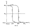
- FIG. 15 is a diagram illustrating the basic constitution of a hysteresis-type input circuit used in digital circuits in the prior art.
- FIG. 17 is a diagram illustrating the waveforms of various portions of said input circuit.
- Hysteresis circuit 100 contained in said hysteresis-type input circuit has the hysteresis-type input/output transmission characteristic shown in FIG. 16 . More specifically, for voltage V in of input signal S in , a lower trip point LTP (lower trip point) having a prescribed value and an upper trip point UTP (upper trip point) having a prescribed value exist. When input voltage V in rises from the L level stable value or minimum value LV in (usually 0 V) to the H level stable value or maximum value HV in , UTP becomes the threshold.
- a first output inversion operation is performed with inversion of output voltage V a from the H level to the L level at UTP.
- a second output inversion operation is performed with inversion of output voltage V a from the L level to the H level at LTP.
- the state in the circuit when said first output inversion operation is performed (the first state) and the state in the circuit when the second output inversion operation is performed (the second state) are different from each other. After performing the first output inversion operation, transition occurs to the second state. After performing the second output inversion operation , transition occurs to the first state. Said transitions are not performed instantly, and there is a time-delay before completion.
- inverter 102 As shown in FIG. 15 , in the conventional hysteresis-type input circuit, on the output side of hysteresis circuit 100, one or several stages of inverter 102 (three stages in the example shown in the figure: (102A), (102B), (102C)) for waveform shaping or line driving are set in a cascade connection.
- in hysteresis circuit 100 when output voltage V a is changed from the L level to the H level or from the H level to the L level with input voltage V in at LTP or UTP, it passes by the inversion threshold of the downstream inverter, especially the inversion threshold Vt a of the first stage inverter (102A).
- the logic level of output voltage V b of inverter (102A) is inverted.
- the same output inversion operation is performed as a chain, and, in the output of the last stage inverter (102C), binary signal S out having voltage V d of the same logic level as that of voltage V in of input signal S in in the steady or DC (direct current) state.
- hysteresis circuit 100 performs a second output inversion operation.
- the output inversion operations are performed as a chain, and voltage V d of output signal S out is changed from the hitherto H level to the L level.
- transition starts from the hitherto state, that is, the second state, to the first state as the state in which the first output inversion operation can be performed at UTP.
- downstream inverters (102A), (102B), (102C) perform output inversion operations as a chain, and voltage V d of output signal S out returns from the H level to the L level.
- an undesired pulse or glitch pulse np corresponding to glitch G 3 is transmitted to the downstream circuit, not shown in the figure.
- inverters (102A), (102B), (102C) When the operation of inverters (102A), (102B), (102C) is delayed, it becomes impossible to follow the minuscule-yet-fast change as a glitch. Consequently, it is also possible to mask a glitch pulse with said inverters.
- transistors With progress in semiconductor process technology in recent years, transistors have achieved higher-speed operation, and it is quite possible that a glitch pulse will pass and be transmitted to a downstream or internal circuit.
- a general object of the present invention is to solve the problems of the prior art by providing a hysteresis-type input circuit characterized by the fact that for any glitch riding on the voltage waveform of the input signal, it can always guarantee stable hysteresis characteristic, and an undesired pulse waveform will not be transmitted to the downstream circuit.
- a hysteresis-type input circuit characterized by the fact that it has a hysteresis circuit, which has a first trip point that has a prescribed value at which the voltage of the output signal with respect to the voltage of the input signal is changed from a second logic level to a first logic level, and a second trip point that has a prescribed value at which the voltage is changed from the first logic level to the second logic level, and which undergoes bidirectional transition with a time-delay between the first state in which operation is performed at said first trip point and the second state in which operation is performed at said second trip point, and it has a transmission control part that performs the following operation: in said hysteresis circuit, when transition is made from said first state to said second state or from said second state to said first state, it prohibits or delays transmission of the output signal of said hysteresis circuit to the downstream circuit before said transition has been essentially completed.
- a hysteresis-type input circuit characterized by the fact that it has a hysteresis circuit, which has a first trip point that has a prescribed value at which the voltage of the output signal with respect to the voltage of the input signal is changed from a second logic level to a first logic level, and a second trip point that has a prescribed value at which the voltage is changed from the first logic level to the second logic level, and which performs transition to a second operable state at said second trip point after performing the first output inversion operation at said first trip point, and transition to a first operable state at said first trip point after performing said second output inversion operation at said second trip point, and it has a transmission control part that performs the following operation: in said hysteresis circuit, when said first output inversion operation or second output inversion operation is performed, it prohibits or delays transmission of the output signal of said hysteresis circuit of said hysteresis circuit to the downstream circuit before the transition
- the operating state in the hysteresis circuit is monitored with a transmission control part. Especially, the state of essentially complete transition from the start of the output inversion operation at the normal trip point to the next stable state (first state or second state) is detected. At this time, the output signal of the hysteresis circuit is transmitted to the downstream circuit.
- said transmission control part detects the timing at which said transition has been essentially completed according to the potential of a prescribed node in said hysteresis circuit.
- said transmission control part has a first inverter, which has a first inversion threshold corresponding to said first trip point, and which outputs a first logic level when the potential of said prescribed node is lower than said first inversion threshold, and outputs a second logic level when said potential of said prescribed node is higher than said first inversion threshold, and a second inverter, which has a second inversion threshold corresponding to said second trip point, and which outputs a first logic level when the potential of said prescribed node is lower than said second inversion threshold, and outputs a second logic level when said potential of said prescribed node is lower than said second inversion threshold; the timing at which the outputs of said first inverter and second inverter are changed from the same logic level to different logic levels is adopted as the first timing; the timing at which the outputs of said first inverter and second inverter are changed from different logic levels to the same logic level is adopted as the second timing, and, with said second timing, the timing is adopted as that at which said transition has
- said first inversion threshold is set with respect to said first trip point at a value that is offset to the side opposite said second trip point side
- said second inversion threshold is set with respect to said second trip point at a value that is offset to the side opposite said first trip point side
- said hysteresis circuit has a third inverter that has said input signal input to its input terminal and has its output terminal connected to a first node, a fourth inverter that has its input terminal connected to said first node and its output terminal connected to a second node, and a fifth inverter that has its input terminal connected to said second node and its output terminal connected to said first node.
- said fifth inverter is composed of a MOS transistor of a first electroconductive type connected between a first power source voltage terminal and said first node and a MOS transistor of a second electroconductive type connected between a second power source voltage terminal and said first node; the threshold of said MOS transistor of said first electroconductive type is defined by one of said first trip point or second trip point, and the threshold of said MOS transistor of said second electroconductive type is defined by the other of said first trip point and second trip point.
- said transmission control part detects the timing at which said transition has been essentially completed in said hysteresis circuit according to the potential of said second node.
- said transmission control part has a sixth inverter having its input terminal connected to said first node, and it detects the timing at which said transition has been essentially completed in said hysteresis circuit according to the potential of the output node of said sixth inverter. In this case, it is possible to set the load of the second node at a small value and to improve the speed of said transition. In addition, said transmission control part detects the timing at which said transition has been essentially completed in said hysteresis circuit according to the potential of said first node.
- said transmission control part has a gate circuit set in the signal transmission path on the downstream side of said hysteresis circuit, and it cuts off said gate circuit when said first output inversion operation or second output inversion operation is started, and it turns ON said gate circuit after said transition has been essentially completed.
- said transmission control part has a driver that drives the signal transmission path on the downstream side to the first logic level or the second logic level corresponding to the potential of the prescribed node of said hysteresis circuit.
- it provides a hysteresis-type input circuit characterized by the following facts: it has a first inverter that has its input terminal connected to a signal input terminal and its output terminal connected to a first node, a second inverter that has its input terminal connected to said first node and its output terminal connected to a second node, a third inverter that has its input terminal connected to said second node and its output terminal connected to said first node, a fourth inverter that has its input terminal connected to said second node and its output terminal connected to a third node, a fifth inverter that has its input terminal connected to said second node and its output terminal connected to a fourth node, a first transistor and a second transistor connected in series between a first power source terminal and an output terminal, and a third transistor and a fourth transistor connected in series between a second power source terminal and said output terminal; the gate terminals of said first transistor and said fourth transistor are connected to said third node; the gate terminals of said second transistor
- the threshold voltage of said fourth inverter be lower than that of said fifth inverter.
- said first transistor and second transistor are pMOS transistors; said third transistor and fourth transistor are nMOS transistors, and a midpoint connection between the drain terminal of said second transistor and the drain terminal of said fourth transistor is connected to said output terminal.
- 10 represents a hysteresis circuit, 12 a transmission control part, 14 a transition-detecting part, 16 a signal transmission path, 18 a gate circuit (transmission gate), 20 a driver, 30 a hysteresis-type input circuit, 40, 42, and 44 inverters, 46 a pMOS transistor, 48 a nMOS transistor, 50, 52, and 54 inverters, 56 a node keeper, 60 an inverter, 62 an inverter, 64 an EXOR circuit, 70 and 72 pMOS transistors, 74 and 76 nMOS transistors, 80 an inverter and N A , N B , N C , N D , N E and N F nodes.
- the hysteresis-type input circuit of the present invention due to the aforementioned constitution and operation, even when glitches and noises are riding on the voltage waveform of the input signal, the hysteresis characteristic can always be guaranteed, so that an undesired pulse waveform will not be transmitted to the downstream circuit.
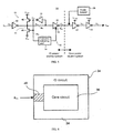
- FIGS. 1 and 2 illustrate basic constitutions of the hysteresis-type input circuit of the present invention.
- the hysteresis-type input circuit of the present invention has hysteresis circuit 10 having a hysteresis-type input/output transmission characteristic shown in FIG. 3 or 4 , and transmission control part 12 that controls signal transmission on the output side corresponding to the timing of the output inversion operation and transition between states of said hysteresis circuit 10.
- Hysteresis circuit 10 has digital signal S in (input voltage V in ) having binary logic levels (H level/L level) input to it, and it outputs output voltage V out having binary logic levels.
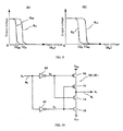
- hysteresis circuit 10 performs a first output inversion operation such that output voltage V out is changed from the H level to the L level ( FIG. 3 ) or from the L level to the H level ( FIG. 4 ) at the UTP as input voltage V in rises from the L level to the H level, and it performs a second output inversion operation such that output voltage V out is changed from the L level to the H level ( FIG. 3 ) or from the H level to the L level ( FIG. 4 ) at the LTP as input voltage V in falls from the H level to the L level.
- the state in hysteresis circuit 10 (first state) when the first output inversion operation is performed and the state in hysteresis circuit 10 (second state) when the second output inversion operation is performed at the LTP are different from each other.
- first state when the first output inversion operation is performed
- second state when the second output inversion operation is performed at the LTP are different from each other.
- UTP after performing the first output inversion operation
- a transition to the second state occurs.
- LTP after performing the second output in version operation, a transition to the first state occurs.
- Transmission control part 12 has transition-detecting part 14 that performs the following operation: in hysteresis circuit 10, each time said first output inversion operation or second output inversion operation is performed, immediately after the operation, the timing at which transition has been essentially completed to the second state or to the first state (hereinafter to be referred to as "transition-completion timing") is detected.
- transmission control part 12 has gate circuit 18 that controls signal transmission on signal transmission path 16 on the output side of hysteresis circuit 10.
- transition-detecting part 14 detects the timing of the start of the first output inversion operation or the second output inversion operation and the transition-completion timing according to the potential of a prescribed node other than the output node in hysteresis circuit 10.
- Gate circuit 18 receives a timing detection signal from transition-detecting part 14, essentially blocks signal transmission path 16 in order to prohibit or delay transmission of signal to the downstream circuit in the period from the timing of the start of the output inversion operation to the transition-completion timing, and, after the transition-completion timing, it sets signal transmission path 16 in the enable state, and re -starts signal transmission to the downstream circuit.
- transmission control part 12 has driver 20 that drives signal transmission path 16 on the output side of hysteresis circuit 10.
- transition-detecting part 14 detects the transition-completion timing according to the potential of the output node, that is, output signal, V out , in hysteresis circuit 10.
- Driver 20 receives a timing detection signal from transition-detecting part 14, and, corresponding to output signal V out of hysteresis circuit 10 after the transition-completion timing, it drives the potential on signal transmission path 16 on the downstream side to the H level or L level.
- FIGS. 1 and 2 are merely examples of the present invention.
- the present invention may have other embodiments.
- one may replace gate circuit 18 of transmission control part 12 with driver 20.
- the hysteresis-type input circuit of the present invention when a normal output inversion operation is started upon input voltage V in reaching the LTP or UTP, even if a glitch (especially a glitch running near the LTP or UTP) is contained in input voltage V in during the transition time before transition to the next stable state has been essentially completed, the glitch can be entirely disregarded or masked, and it is possible to prevent transmission of a desired pulse to the downstream circuit with high reliability.
- FIG. 5 is a diagram illustrating the circuit constitution of hysteresis-type input circuit 30 in an embodiment of the present invention.
- This input circuit 30, for example, is set in IO circuit 38 on the periphery of core circuit 36 at the center portion of semiconductor chip 34 of the digital IC shown in FIG. 6 , and it acts as a receiver circuit for input of digital signal S in from the outside.
- hysteresis circuit 10 in this embodiment is composed of three inverters 40, 42, 44.
- Inverter 40 has input signal S in input to its input terminal, and has its output terminal connected to node N A .
- Inverter 42 has its input terminal connected to node N A and its output terminal connected to node N B .
- Inverter 44 has its input terminal connected to N B and its output terminal connected to node N A .
- Inverter 44 is composed of pMOS transistor 46 and nMOS transistor 48.
- pMOS transistor 46 has its source terminal connected to the terminal of power source voltage V DD1 on the positive electrode side, its drain terminal connected to node N A , and its gate terminal connected to node N B .
- nMOS transistor 48 has its source terminal connected to the terminal of power source voltage V SS (conventional ground potential) on the negative electrode side, its drain terminal connected to node N A , and its gate terminal connected to node N B .
- V SS conventional ground potential
- FIG. 7 is a diagram illustrating the input/output characteristic of said hysteresis circuit 10 in said embodiment.
- the input/output characteristic in this case is of the type shown in FIG. 3 (input/output inversion type).
- Solid curve M O shows the input/output characteristic of hysteresis circuit 10 excluding inverter 44 (as a result, inverter 42 is also excluded), that is, the input/output characteristic of inverter 40.
- trip point TP 0 corresponds to the inversion threshold of inverter 40.
- Dot-dash curve M P shows the input/output characteristic of hysteresis circuit 10 with only nMOS transistor 48 of inverter 44 excluded.
- the trip point in said input/output characteristic M P is upper trip point UTP of hysteresis circuit 10, and the hysteresis width in this case (UTP -TP 0 ) is determined by the current-driving ability of pMOS transistor 46.
- Double-dot-dash curve M N shows the input/output characteristic when only pMOS transistor 46 of inverter 44 is excluded from hysteresis circuit 10.
- the trip point of said input/output characteristic M N is lower trip point LTP of hysteresis circuit 10.
- the hysteresis width in this case (TP 0 -LTP) is determined by the current-driving ability ofnMOS transistor 48.
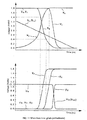
- Inversion threshold Vt A is the threshold when output inversion operation is performed for inverters 42, 50 that have the output voltage or node voltage V A input to them ( FIG. 5 ).
- output voltage V A changes as E ⁇ D ⁇ F ⁇ B ⁇ A.
- output voltage V A changes along input/output characteristic M N .
- output voltage V A rapidly rises from the L level through inversion threshold Vt A to the H level, and there is a jump from input/output characteristic M N to input/output characteristic M P (F ⁇ B).
- input/output characteristic M P output voltage V A rises to stable value HV A (B ⁇ A).
- hysteresis circuit 10 in this embodiment when the first output inversion operation is performed with output voltage V A inverted from the H level to the L level at the UTP, that is, in the first state, in inverter 44, pMOS transistor 46 is ON, while nMOS transistor 48 is OFF.
- the second output inversion operation when the second output inversion operation is performed, with output voltage V A inverted from the L level to the H level at the LTP, that is, in the second state, in inverter 44, pMOS transistor 46 is OFF, while nMOS transistor 48 is ON.
- transition to the second state occurs (the state in which in inverter 44, pMOS transistor 46 is OFF, while nMOS transistor 48 is ON).
- point E stable value
- transition to the first state occurs (the state in which for inverter 44, pMOS transistor 46 is ON, while nMOS transistor 48 is OFF).
- the effective operation point of the trip point in hysteresis circuit 10 undergoes transition from the LTP to the UTP.
- This transition is performed as a floating UTP' that allows the same abnormal output inversion operation as the first output inversion operation undergoes transition (rises) from the position (value) of the LTP to the position (value) of the UTP, and, when the UTP' reaches the UTP, the operation comes to an end.
- Said transition of the effective operation point of the trip point from the LTP to the UTP corresponds to the transition to the first state immediately after said second output inversion operation .
- node N B in hysteresis circuit 10 is connected to the input terminal of transition-detecting part 14 of transmission control part 12.
- Transition-detecting part 14 can detect the timing of the start of the output inversion operation and the timing of transition-completion in hysteresis circuit 10 corresponding to potential V B of node N B .
- gate circuit 18 of transmission control part 12 may be set on the signal transmission path connected to output node N A of hysteresis circuit 10, such as inside, upstream or downstream of inverter 50 of the IO power source system (V DD1 : such as 1.8 V).
- inverters 52, 54 of the core power source system (V DD2 : such as 1.1 V) are connected as two cascade stages in the downstream of inverter 50.
- node keeper 56 for preventing a floating state of the signal transmission path at an appropriate position on the signal transmission path, such as between inverter 50 and inverter 52.
- FIG. 8 is a diagram illustrating a specific example constitution of transition -detecting part 14 and gate circuit 18 of transmission control part 12.
- Transition-detecting part 14 has the following components: a pair of inverters 60, 62 having their input terminals connected to node N B of hysteresis circuit 10, exclusive-OR (EXOR) circuit 64 that performs computation of the exclusive-OR for output voltages V X and V Y of inverters 60, 62, and inverter 66 that performs inversion for the output of said EXOR circuit 64.
- EXOR exclusive-OR
- Inverters 60, 62 have the input/output characteristics shown in FIGS. 9(A), (B) , respectively.
- threshold TC 60 in the input/output characteristic (solid curve K 60 ) of inverter 60 is much lower than threshold TC 0 of the input/output characteristic of a conventional inverter (dot-dash curve K 0 ), and it is set near the LTP of hysteresis circuit 10 (or preferably a value smaller than the LTP).
- Inverter input/output characteristic K 60 having said rather small threshold TC 60 can be realized by adjusting the balance of the current-driving ability of the pMOS transistor and nMOS transistor that form inverter 60 (that is, by having that of the nMOS side higher than that of the pMOS side).
- threshold TC 62 in the input/output characteristic (solid curve K 62 ) of inverter 62 is significantly higher than threshold TC 0 of the conventional inverter input/output characteristic (dot-dash curve K 0 ), and it is set at a value near the UTP of hysteresis circuit 10 (preferably a value larger than the UTP).
- Said inverter input/output characteristic K 62 having a rather high threshold TC 62 can be realized by adjusting the balance in the current-driving ability of the pMOS transistor and nMOS transistor that form inverter 62 (by having that of the pMOS side higher than that of the nMOS side).
- gate circuit 18 consists of a transmission gate.
- said transmission gate 18 When the output of transition-detecting part 14 is at the H level, said transmission gate 18 is ON, so that voltage signal V A on node N A is transmitted to the input terminal of inverter 50.
- transmission gate 18 When the output of transition-detecting part 14 is at the L level, transmission gate 18 is OFF, and, in the high -impedance state, voltage signal V A on node N A is cut off.
- FIG. 10 is a diagram illustrating another example constitution of transmission control part 12.
- transition-detecting part 14 is composed of only said initial inverters 60, 62, and driver 20 consists of inverter 50.
- inverter 50 is composed of two pMOS transistors 70, 72 connected in series between the terminal of power source voltage V DD1 on the positive electrode side and output-side node N C , and two nMOS transistors 74, 76 connected in series between output-side node N C and the terminal of power source voltage V SS on the negative electrode side.
- inverter 60 The output terminal of inverter 60 is connected to the gate terminals of pMOS transistor 70 and nMOS transistor 74, and the output terminal of inverter 62 is connected to the gate terminals of pMOS transistor 72 and nMOS transistor 76.
- node N B of hysteresis circuit 10 acts as both a monitor node and an output node, and it is connected to the input terminal of transition-detecting part 14 (inverters 60, 62).
- Transmission control part 12 has the advantage that since the number of structural members is less, the time-delay of the operation is shorter.
- hysteresis-type input circuit 30 in this embodiment will be explained with reference to the waveform figures shown in FIGS. 11 and 12 .
- FIG. 11 is a diagram illustrating operation without a glitch rising during falling of input voltage V in from the H level to the L level.
- potential V B of node N B in hysteresis circuit 10 starts falling from the level (1.8 V) of power source voltage V DD1 , and it quickly falls towards the level (0 V) of power source voltage V SS .
- Potential V A of node N A also rises rapidly from near the level of V SS towards the level (1.8 V) of V DD1 , and it is inverted during this from the L level to the H level.
- inverter 44 of hysteresis circuit 10 there is a transition from the state (second state) in which nMOS transistor 48 is ON and pMOS transistor 46 is OFF to the state (first state) in which nMOS transistor 48 is OFF and pMOS transistor 46 is ON.
- potential V B of node N B of hysteresis circuit 10 is input to inverters 60, 62 of transition-detecting part 14. Before input voltage V in falls from the H level to the L level, potential V B of node N B is kept at the V DD1 level. Consequently, outputs of both inverters 60, 62 are at the L level. Consequently, in the example constitution shown in FIG. 8 , in transition-detecting part 14, the output of EXOR circuit 64 is at the L level, and the output of inverter 66 is at the H level. Consequently, transmission gate 18 on the signal transmission path is ON, and voltage V A of node N A is input or transmitted to inverter 50. In the example constitution shown in FIG. 10 , in inverter 50, both pMOS transistors 70, 72 are turned ON, and both nMOS transistors 74, 76 are turned OFF, and output-side N C is driven to the level of V DD1 .
- node potential V B of hysteresis circuit 10 crosses threshold TC 62 (about 1.4 V) of inverter 62, and at this timing, output voltage V Y of inverter 62 rapidly rises from the V SS level (0 V) to the V DD1 level (about 1.8 V).
- inverters 52, 54 of the downstream core power source system also perform output inversion operation as a chain, output voltage V D of inverter 52 is inverted from the V SS level (0 V) to the V DD2 level (1.1 V), and output voltage V E of inverter 54 is inverted from the V DD2 level (1.1 V) to the V SS level (0 V). Also, in FIG. 11 , in order to facilitate explanation, the time-delay of transition-detecting part 14 in the example constitution shown in FIG. 8 is ignored.
- inverter 50 when output voltages V X , V Y of both inverters 60, 62 reach the H level, in inverter 50, both pMOS transistors 70, 72 are turned OFF, and both nMOS transistors 74, 76 are turned ON, and output-side node N C is driven to the level of V SS .
- inverters 52, 54 of the downstream core power source system also perform output inversion operation s as a chain.
- Output voltage V D of inverter 52 is inverted from the V DD2 level (1.1 V) to the V SS level (0 V), and output voltage V E of inverter 54 is inverted from the V SS level (0 V) to the V DD2 level (1.1 V).
- FIG. 12 is a diagram illustrating operation in case glitch G rides near the LTP as input voltage V in falls from the H level to the L level.
- V in passes the LTP (about 0.8 V)
- potential V B of node N B in hysteresis circuit 10 quickly falls from the V DD1 level (1.8 V)
- potential V A of node N A rises quickly towards the V DD1 level (1.8 V).
- due to zigzag glitch G immediately after input voltage V in crosses the LTP, it turns to rise and then soon returns to falling, and it falls to the V SS level (0 V).
- potential V B of node N B first falls rapidly and then stops halfway, and it turns back to rise near the V DD1 level (1.8 V). Then, it turns to fall, and it falls to the V SS level (0 V). Also, potential V A of node N A stops the initial rapid rise and it returns to falling, followed by rising again, and it rises to the V DD1 level (1.8 V).
- V B of node N B falls again and falls to the V SS level (0 V)
- V SS level (0 V)
- threshold TC 62 about 1.4 V
- inverter 62 performs an output inversion operation, and output voltage V Y is inverted from the L level to the H level.
- potential V B of node N B crosses threshold TC 60 (about 0.4 V) of inverter 60
- inverter 60 performs an output inversion operation, and output voltage V X is inverted from the L level to the H level.
- inverters 52, 54 of the downstream core power source system also perform output inversion operation s as a chain, output voltage V D of inverter 52 is inverted from the V SS level (0 V) to the V DD2 level (1.1 V), and output voltage V E of inverter 54 is inverted from the V DD2 level (1.1 V) to the V SS level (0 V).
- output voltage V Y of inverter 62 is inverted from the L level to the H level, and, in inverter 50, pMOS transistor 70 and nMOS transistor 76 are turned ON, pMOS transistor 72 and nMOS transistor 74 are turned OFF, and output-side node N C enters the high-impedance state.
- output voltage V X of inverter 60 is inverted from the L level to the H level, and, in inverter 50, both pMOS transistors 70, 72 are turned OFF, both nMOS transistors 74, 76 are turned ON, and output-side node N C is driven to the V SS level (0 V).
- output inversion operation s are performed as a chain, output voltage V D of inverter 52 is inverted from the V SS level (0 V) to the V DD2 level (1.1 V), and output voltage V E of inverter 54 is inverted from the V DD2 level (1.1 V) to the V SS level (0 V).
- FIG. 13 As a reference (Comparative Example), transmission control part 12 from hysteresis-type input circuit 30 in FIG. 5 is omitted, and the operation with input voltage V in having the same glitch G as aforementioned is displayed.
- transmission control part 12 because transmission control part 12 is not connected to node N B , the load of inverter 42 decreases. As a result, potential V B of node N B varies faster and the change is significant.
- inverter 50 is assumed to work with the same load as that of inverter 42, and potential V C of output-side node N C of inverter 50 deemed to vary with the same value s as those of potential V B of node N B .
- V A of node N A tracks glitch G, and it is input or transmitted to inverter 50 as is, so that inverter 50, and then downstream inverters 52, 54 also operate corresponding to glitch G in the output inversion operation, and glitch pulse np appears as noise on the waveform of output S out .
- FIG. 14 is a diagram illustrating the constitution of hysteresis-type input circuit 30 in Embodiment 2 of the present invention.
- node N A in the hysteresis-type input circuit ( FIG. 5 ) in said Embodiment 1 is connected to the input terminal of inverter 80, and the output terminal of inverter 80 is connected to the input terminal of transmission control part 12.
- inverter 80 be designed with the same circuit constant as that of inverter 42.
- the load connected to output node N F of inverter 80 is definitely higher than the load on the side of node N B (inverter 44), and potential V F of node N F is designed to change, with certainty, slower than potential V B of node N B .
- Embodiment 2 by reducing the load of node N B , after the output inversion operation in hysteresis circuit 10, it is possible to increase the speed of transition to the first or second state. More strictly speaking, because the load of node N A is increased, there is a definite increase in the signal transmission delay, yet there is no influence on the relative timing relationship between the transition in hysteresis circuit 10 and the delay in transmission to the downstream circuit.
- inverter 80 may omit inverter 80 and have node N A directly connected to the input terminal of transmission control part 12.
- the embodiment shown in FIG. 6 is merely an example, and the hysteresis-type input circuit of the present invention can be used in any digital circuit or digital signal processing.
Landscapes
- Manipulation Of Pulses (AREA)
- Logic Circuits (AREA)
Claims (9)
- Un circuit d'entrée du type à hystérésis comprenant :un circuit d'hystérésis (10) qui a un premier point de déclenchement qui a une valeur prescrite à laquelle la tension du signal de sortie par rapport à la tension du signal d'entrée est changée d'un deuxième niveau logique à un premier niveau logique, et un deuxième point de déclenchement qui a une valeur prescrite à laquelle la tension est changée du premier niveau logique au deuxième niveau logique, et qui subit une transition bidirectionnelle avec un temps de retard entre un premier état dans lequel le fonctionnement est effectué audit premier point de déclenchement et un deuxième état dans lequel le fonctionnement est effectué audit deuxième point de déclenchement;une partie de commande de transmission (12) qui, quand la transition dudit premier état audit deuxième état ou dudit deuxième état audit premier état dans dudit circuit d'hystérésis se passe, prohibe ou retarde la transmission du signal de sortie dudit circuit d'hystérésis à un circuit aval avant ladite transition a été achevée ;caractérisé en ce que ledit circuit d'hystérésis comprendun troisième inverseur (40) qui a ledit signal d'entrée donné à son terminal d'entrée et qui a son terminal de sortie lié à un premier noeud (NA),un quatrième inverseur (42) qui a son terminal d'entrée lié audit premier noeud et son terminal de sortie lié à un deuxième noeud (NB),un cinquième inverseur (44) qui a son terminal d'entrée lié audit deuxième noeud et son terminal de sortie lié audit premier noeud : et oùledit cinquième inverseur comprend un transistor MOS d'un premier type électro-conducteur(46) lié entre un premier terminal de source de tension d'alimentation et ledit premier noeud, et un transistor MOS d'un deuxième type électro-conducteur (48) lié entre un deuxième terminal de source de tension d'alimentation et ledit premier noeud ;
Le seuil dudit transistor MOS du premier type électro-conducteur est défini par un desdits premier ou deuxième points de déclenchement, et le seuil dudit transistor MOS dudit deuxième type électro-conducteur est défini par l'autre l'un desdits premier et deuxième points de déclenchement. - Le circuit d'entrée du type à hystérésis selon la revendication 1 caractérisé en ce que ladite partie de commande de transmission détecte la synchronisation à laquelle ladite transition a été essentiellement achevée selon le potentiel d'un noeud prescrit dans un circuit d'hystérésis.
- Le circuit d'entrée du type à hystérésis selon la revendication 2 caractérisé en ce que :ladite partie de commande de transmission comprendun premier inverseur, qui a un premier seuil d'inversion qui correspond audit premier point de déclenchement, et qui sort le premier niveau logique quand le potentiel dudit noeud prescrit est moins que ledit premier seuil d'inversion, et sort le deuxième niveau logique quand ledit potentiel dudit noeud prescrit est plus haut que ledit premier seuil d'inversion,un deuxième inverseur, qui a un deuxième seuil d'inversion qui correspond audit deuxième point de déclenchement, et qui sort le premier niveau logique quand le potentiel dudit noeud prescrit est moins que ledit deuxième seuil d'inversion, et sort le deuxième niveau logique quand ledit potentiel dudit noeud prescrit est moins que ledit deuxième seuil d'inversion ;la synchronisation à laquelle les sorties dudit premier inverseur et dudit deuxième inverseur sont changées du même niveau logique aux niveaux de logique différents est adoptée comme la première synchronisation ; la synchronisation à laquelle les sorties des premier et deuxième inverseurs sont changées des niveaux de logique différents au même niveau de logique est adoptée comme la deuxième synchronisation, et, avec ladite deuxième synchronisation, la synchronisation est adoptée comme cela à laquelle ladite transition a été substantiellement achevée.
- Le circuit d'entrée du type à hystérésis selon la revendication 3 caractérisé en ce que :ledit premier seuil d'inversion est établi par rapport au premier point de déclenchement à une valeur qui est offset au côté en face du côté dudit deuxième point de déclenchement ;ledit deuxième seuil d'inversion est établi par rapport au deuxième point de déclenchement à une valeur qui est offset au côté en face du côté dudit premier point de déclenchement.
- Le circuit d'entrée du type à hystérésis selon les revendications 1-4 caractérisé en ce que la partie de commande de transmission détecte la synchronisation à laquelle ladite transition a été essentiellement achevée dans ledit circuit d'hystérésis selon le potentiel dudit deuxième noeud.
- Le circuit d'entrée du type à hystérésis selon les revendications 1-4 caractérisé en ce que la partie de commande de transmission a un sixième inverseur ayant son terminal d'entrée lié audit premier noeud, et elle détecte la synchronisation à laquelle ladite transition a été essentiellement achevée dans ledit circuit d'hystérésis selon le potentiel dudit noeud de sortie du sixième inverseur.
- Le circuit d'entrée du type à hystérésis selon les revendications 1-4 caractérisé en ce que la partie de commande de transmission détecte la synchronisation à laquelle ladite transition a été essentiellement achevée dans ledit circuit d'hystérésis selon le potentiel dudit premier noeud.
- Le circuit d'entrée du type à hystérésis selon les revendications 2-7 caractérisé en ce que la partie de commande de transmission a un circuit de grille posé dans I voie de transmission du signal sur le côté en aval dudit circuit d'hystérésis, et elle coupe ledit circuit de grille quand ledit premier fonctionnement d'inversion de sortie ou le deuxième fonctionnement d'inversion de sortie est commencé, et elle met en marche ledit circuit de grille après la transition a été substantiellement achevée.
- Le circuit d'entrée du type à hystérésis selon les revendications 1-8 caractérisé en ce que la partie de commande de transmission a un driver qui pilote la voie de transmission du signal sur le côté en aval au premier niveau logique ou le deuxième niveau de logique correspondant au potentiel du noeud prescrit dudit circuit d'hystérésis.
Applications Claiming Priority (2)
| Application Number | Priority Date | Filing Date | Title |
|---|---|---|---|
| JP2004033239A JP3809585B2 (ja) | 2004-02-10 | 2004-02-10 | ヒステリシス型入力回路 |
| JP2004033239 | 2004-02-10 |
Publications (3)
| Publication Number | Publication Date |
|---|---|
| EP1564885A2 EP1564885A2 (fr) | 2005-08-17 |
| EP1564885A3 EP1564885A3 (fr) | 2006-06-07 |
| EP1564885B1 true EP1564885B1 (fr) | 2014-01-15 |
Family
ID=34697874
Family Applications (1)
| Application Number | Title | Priority Date | Filing Date |
|---|---|---|---|
| EP05100957.9A Ceased EP1564885B1 (fr) | 2004-02-10 | 2005-02-10 | Un circuit d'entrée à hystérésis |
Country Status (3)
| Country | Link |
|---|---|
| US (1) | US7365586B2 (fr) |
| EP (1) | EP1564885B1 (fr) |
| JP (1) | JP3809585B2 (fr) |
Families Citing this family (5)
| Publication number | Priority date | Publication date | Assignee | Title |
|---|---|---|---|---|
| US8031053B2 (en) * | 2007-10-26 | 2011-10-04 | Round Rock Research, Llc | RFID label time synchronization |
| KR101171561B1 (ko) * | 2010-09-29 | 2012-08-06 | 삼성전기주식회사 | 펄스 폭에 따라 동작하는 슈미트 트리거 회로 |
| US11146253B1 (en) * | 2020-08-24 | 2021-10-12 | Electronics And Telecommunications Research Institute | Receiving circuit to process low-voltage signal with hysteresis |
| CN112821882B (zh) * | 2020-12-30 | 2023-09-12 | 国家超级计算无锡中心 | 可切换工作点的高性能施密特触发器及切换工作点方法 |
| US20230327652A1 (en) * | 2022-04-11 | 2023-10-12 | Renesas Electronics Corporation | Semiconductor device and input signal controlling method |
Family Cites Families (9)
| Publication number | Priority date | Publication date | Assignee | Title |
|---|---|---|---|---|
| US5113098A (en) * | 1991-03-29 | 1992-05-12 | Advanced Micro Devices, Inc. | Glitch remover circuit for transmission links |
| US5459437A (en) * | 1994-05-10 | 1995-10-17 | Integrated Device Technology | Logic gate with controllable hysteresis and high frequency voltage controlled oscillator |
| JPH08162923A (ja) * | 1994-11-30 | 1996-06-21 | Unisia Jecs Corp | ノイズ除去装置 |
| US5595361A (en) * | 1995-11-22 | 1997-01-21 | Abc Rail Products Corporation | Wing rail hold-down |
| KR100253273B1 (ko) * | 1996-10-29 | 2000-04-15 | 김영환 | 입력 버퍼 회로 |
| US5878094A (en) * | 1997-06-10 | 1999-03-02 | International Business Machines Corporation | Noise detection and delay receiver system |
| US5949265A (en) * | 1997-10-31 | 1999-09-07 | International Business Machines Corporation | Soft latch circuit having sharp-cornered hysteresis characteristics |
| FR2777717B1 (fr) * | 1998-04-17 | 2002-12-06 | Sextant Avionique | Circuit pour l'acquisition de signaux analogiques binaires |
| US6433602B1 (en) * | 2000-08-30 | 2002-08-13 | Lattice Semiconductor Corp. | High speed Schmitt Trigger with low supply voltage |
-
2004
- 2004-02-10 JP JP2004033239A patent/JP3809585B2/ja not_active Expired - Fee Related
-
2005
- 2005-02-10 US US11/056,288 patent/US7365586B2/en not_active Expired - Lifetime
- 2005-02-10 EP EP05100957.9A patent/EP1564885B1/fr not_active Ceased
Also Published As
| Publication number | Publication date |
|---|---|
| EP1564885A2 (fr) | 2005-08-17 |
| US20050218950A1 (en) | 2005-10-06 |
| EP1564885A3 (fr) | 2006-06-07 |
| JP2005229171A (ja) | 2005-08-25 |
| US7365586B2 (en) | 2008-04-29 |
| JP3809585B2 (ja) | 2006-08-16 |
Similar Documents
| Publication | Publication Date | Title |
|---|---|---|
| US7511555B2 (en) | Level conversion circuit and input-output device using same | |
| US5081377A (en) | Latch circuit with reduced metastability | |
| US9966955B2 (en) | Overdrive receiver circuitry | |
| KR930000972B1 (ko) | Cmos인버터를 구비한 반도체 집적회로 | |
| US6791392B2 (en) | Circuit for shifting an input signal level including compensation for supply voltage variation | |
| US6853228B2 (en) | Flip-flop circuit | |
| US6351149B1 (en) | MOS transistor output circuit | |
| US6617881B2 (en) | Semiconductor integrated circuit | |
| EP0458766B1 (fr) | Filtrage des pointes pour des circuits logiques | |
| US6396306B2 (en) | Regenerative tie-high tie-low cell | |
| EP1564885B1 (fr) | Un circuit d'entrée à hystérésis | |
| KR970005574B1 (ko) | 노이즈 감쇠 출력 버퍼 | |
| JP4311887B2 (ja) | 信号処理装置 | |
| US8004307B2 (en) | Static-dynamic-dynamic repeater circuit | |
| US8035425B2 (en) | Active echo on-die repeater circuit | |
| US20040061522A1 (en) | Digital level shifter with reduced power dissipation and false transmission blocking | |
| US7880513B2 (en) | Repeater circuit with staged output | |
| US8030960B2 (en) | Converting dynamic repeaters to conventional repeaters | |
| JP2004364031A (ja) | 半導体集積回路 | |
| JP5452983B2 (ja) | プロセスモニタ回路およびプロセス特性の判定方法 | |
| KR20020091803A (ko) | 씨모스 출력 회로 | |
| JP4413196B2 (ja) | ヒステリシス型入力回路 | |
| JPH09214324A (ja) | Cmos論理回路 | |
| JP2540765B2 (ja) | 誤動作防止テスト回路 | |
| JP2002198795A (ja) | 半導体装置 |
Legal Events
| Date | Code | Title | Description |
|---|---|---|---|
| PUAI | Public reference made under article 153(3) epc to a published international application that has entered the european phase |
Free format text: ORIGINAL CODE: 0009012 |
|
| AK | Designated contracting states |
Kind code of ref document: A2 Designated state(s): AT BE BG CH CY CZ DE DK EE ES FI FR GB GR HU IE IS IT LI LT LU MC NL PL PT RO SE SI SK TR |
|
| AX | Request for extension of the european patent |
Extension state: AL BA HR LV MK YU |
|
| PUAL | Search report despatched |
Free format text: ORIGINAL CODE: 0009013 |
|
| AK | Designated contracting states |
Kind code of ref document: A3 Designated state(s): AT BE BG CH CY CZ DE DK EE ES FI FR GB GR HU IE IS IT LI LT LU MC NL PL PT RO SE SI SK TR |
|
| AX | Request for extension of the european patent |
Extension state: AL BA HR LV MK YU |
|
| 17P | Request for examination filed |
Effective date: 20061207 |
|
| AKX | Designation fees paid |
Designated state(s): DE FR GB |
|
| 17Q | First examination report despatched |
Effective date: 20110531 |
|
| GRAP | Despatch of communication of intention to grant a patent |
Free format text: ORIGINAL CODE: EPIDOSNIGR1 |
|
| INTG | Intention to grant announced |
Effective date: 20130709 |
|
| GRAS | Grant fee paid |
Free format text: ORIGINAL CODE: EPIDOSNIGR3 |
|
| GRAA | (expected) grant |
Free format text: ORIGINAL CODE: 0009210 |
|
| AK | Designated contracting states |
Kind code of ref document: B1 Designated state(s): DE FR GB |
|
| REG | Reference to a national code |
Ref country code: GB Ref legal event code: FG4D |
|
| REG | Reference to a national code |
Ref country code: DE Ref legal event code: R096 Ref document number: 602005042481 Country of ref document: DE Effective date: 20140227 |
|
| REG | Reference to a national code |
Ref country code: DE Ref legal event code: R097 Ref document number: 602005042481 Country of ref document: DE |
|
| PLBE | No opposition filed within time limit |
Free format text: ORIGINAL CODE: 0009261 |
|
| STAA | Information on the status of an ep patent application or granted ep patent |
Free format text: STATUS: NO OPPOSITION FILED WITHIN TIME LIMIT |
|
| 26N | No opposition filed |
Effective date: 20141016 |
|
| REG | Reference to a national code |
Ref country code: DE Ref legal event code: R097 Ref document number: 602005042481 Country of ref document: DE Effective date: 20141016 |
|
| REG | Reference to a national code |
Ref country code: FR Ref legal event code: PLFP Year of fee payment: 12 |
|
| REG | Reference to a national code |
Ref country code: FR Ref legal event code: PLFP Year of fee payment: 13 |
|
| REG | Reference to a national code |
Ref country code: FR Ref legal event code: PLFP Year of fee payment: 14 |
|
| PGFP | Annual fee paid to national office [announced via postgrant information from national office to epo] |
Ref country code: GB Payment date: 20200130 Year of fee payment: 16 Ref country code: DE Payment date: 20200115 Year of fee payment: 16 |
|
| PGFP | Annual fee paid to national office [announced via postgrant information from national office to epo] |
Ref country code: FR Payment date: 20200124 Year of fee payment: 16 |
|
| REG | Reference to a national code |
Ref country code: DE Ref legal event code: R119 Ref document number: 602005042481 Country of ref document: DE |
|
| GBPC | Gb: european patent ceased through non-payment of renewal fee |
Effective date: 20210210 |
|
| PG25 | Lapsed in a contracting state [announced via postgrant information from national office to epo] |
Ref country code: FR Free format text: LAPSE BECAUSE OF NON-PAYMENT OF DUE FEES Effective date: 20210228 Ref country code: GB Free format text: LAPSE BECAUSE OF NON-PAYMENT OF DUE FEES Effective date: 20210210 Ref country code: DE Free format text: LAPSE BECAUSE OF NON-PAYMENT OF DUE FEES Effective date: 20210901 |