EP1563607B1 - Analog-digital wandler für mikrowellen - Google Patents
Analog-digital wandler für mikrowellen Download PDFInfo
- Publication number
- EP1563607B1 EP1563607B1 EP03796026A EP03796026A EP1563607B1 EP 1563607 B1 EP1563607 B1 EP 1563607B1 EP 03796026 A EP03796026 A EP 03796026A EP 03796026 A EP03796026 A EP 03796026A EP 1563607 B1 EP1563607 B1 EP 1563607B1
- Authority
- EP
- European Patent Office
- Prior art keywords
- loop
- loops
- signal
- converter
- bits
- Prior art date
- Legal status (The legal status is an assumption and is not a legal conclusion. Google has not performed a legal analysis and makes no representation as to the accuracy of the status listed.)
- Expired - Lifetime
Links
- 230000015654 memory Effects 0.000 claims abstract description 20
- 230000003287 optical effect Effects 0.000 claims abstract description 6
- 230000003247 decreasing effect Effects 0.000 claims description 3
- 238000006243 chemical reaction Methods 0.000 abstract description 14
- 230000004907 flux Effects 0.000 description 13
- 238000010586 diagram Methods 0.000 description 3
- 230000006870 function Effects 0.000 description 3
- 239000000463 material Substances 0.000 description 3
- 239000004065 semiconductor Substances 0.000 description 3
- 101100406879 Neurospora crassa (strain ATCC 24698 / 74-OR23-1A / CBS 708.71 / DSM 1257 / FGSC 987) par-2 gene Proteins 0.000 description 2
- 238000005259 measurement Methods 0.000 description 2
- 229910052758 niobium Inorganic materials 0.000 description 2
- 239000010955 niobium Substances 0.000 description 2
- GUCVJGMIXFAOAE-UHFFFAOYSA-N niobium atom Chemical compound [Nb] GUCVJGMIXFAOAE-UHFFFAOYSA-N 0.000 description 2
- 238000005070 sampling Methods 0.000 description 2
- 230000006641 stabilisation Effects 0.000 description 2
- 230000005540 biological transmission Effects 0.000 description 1
- 238000001514 detection method Methods 0.000 description 1
- 235000021183 entrée Nutrition 0.000 description 1
- 239000013307 optical fiber Substances 0.000 description 1
- 230000010355 oscillation Effects 0.000 description 1
- 238000013139 quantization Methods 0.000 description 1
- 230000035945 sensitivity Effects 0.000 description 1
- 230000003595 spectral effect Effects 0.000 description 1
- 238000011105 stabilization Methods 0.000 description 1
- 239000002887 superconductor Substances 0.000 description 1
Images
Classifications
-
- H—ELECTRICITY
- H03—ELECTRONIC CIRCUITRY
- H03M—CODING; DECODING; CODE CONVERSION IN GENERAL
- H03M1/00—Analogue/digital conversion; Digital/analogue conversion
- H03M1/12—Analogue/digital converters
- H03M1/34—Analogue value compared with reference values
- H03M1/38—Analogue value compared with reference values sequentially only, e.g. successive approximation type
- H03M1/44—Sequential comparisons in series-connected stages with change in value of analogue signal
Definitions
- the present invention relates to an analog / digital converter for microwaves
- Flash type fast converters are limited in resolution by the complexity of their circuits. Indeed, the number of comparators they comprise is equal to the number of measurement points, ie 256 comparators for an 8-bit encoder. Furthermore, the high-resolution coders are limited in speed because of their operating principle (they generally comprise a 20-bit integrator operating at 50 Hz) or because of their clock frequency (de / ⁇ type encoders at 14). bits operating at 50MHz).
- JP 01051681 discloses an analog / digital converter having N superconducting loops in the path of the wave to be converted having the same inductance but with different critical currents. Each loop has a junction of the Josephson type whose result of the current quantity detection is sent directly to an encoder.
- the present invention relates to an analog / digital converter which is both fast and high resolution, while being able to operate at high frequencies, for example of the order of, or greater than 10 GHz.
- the analog / digital converter according to the invention comprises N superconducting loops disposed in the path of the wave to be converted, these loops being regularly spaced apart by a half-wavelength, each loop comprising a critical current junction. connected by a waveguide an output memory cell, the product of the inductance of each loop by its critical current being equal to a constant.
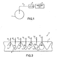
- FIG. 1 shows an "elementary comparator” which is an essential elementary component of the analog / digital converter of the invention.
- This elementary comparator comprises a superconducting loop 1, preferably of circular shape, in which is a critical current junction 2, an optical waveguide 3, and a one-bit output memory cell 4, which is sequenced at the desired acquisition rate.
- the junction 2 is a constriction of a few tens of nanometers or a "gap" practiced in the loop 1 and in which is formed a dielectric layer of a few angstroms thick.
- One of the ends of the guide 3 is arranged almost in contact with the junction 2, while its other end is connected to the memory 4.
- the connection between the guide 3 and the memory 4 is carried out, in a manner known per se, by a sensor 5.
- the memory 4 is part of a set of memory cells (together to which are connected the other loops, as described below with reference to Figure 2). This set of memory cells may be an integrated memory circuit as commonly used in microcomputers.
- the waveguide 3 Since the outputs of the converter of the invention operate at frequencies of the order of one or more terahertz (10 12 Hz), the waveguide 3 must be of a particular type to allow the corresponding optical mode of settle there, and possibly be amplified.
- this waveguide is of the type described in the article by R. K ⁇ HLER et al published in the journal NATURE, Volume 417 (6885) of May 9, 2002, 156-159.
- Loop 1 is arranged in the magnetic field of the signal to be measured. If this signal propagates in an electromagnetic waveguide, the loop is arranged inside this guide. If the signal propagates in a line (for example of the "Strip Line” type), the loop is engraved in this line.
- the Loop 1 thus makes a comparison between the magnetic flux ⁇ n that it receives from the signal to be measured and the reference value ⁇ o that it can absorb.
- This value ⁇ o is an absolute reference, fundamental quantum magnitude (the superconducting material of the loop is immersed in a fixed temperature cryogenic bath).
- the superconducting loop of rank n absorbs flux, and the loop temporarily stores a bit n of value "1".
- the storage of a bit "1" in the loop 1 causes the emission of a voltage pulse, of a duration of the order of one or more picoseconds, through the junction 2. This pulse is sensed by the guide 3 and transmitted in optical form, then converted into voltage by the device 5 and stored by the memory 4.
- the comparator of FIG. 1 makes it possible to perform the function of a 1-bit analog / digital converter.
- the signal to be measured may result either from the sampling of an incident signal by a sample-and-hold device driven by a reference clock, or from the conversion of this incident signal by frequency mixing using a stable local oscillator. oscillating at a frequency F greater than twice the maximum frequency of the incident signal. This latter solution is preferred when the incident signal is a microwave signal with a frequency of the order of 1 GHz to 100 GHz.
- the number of significant bits is determined by the accuracy of the technological realization of the loop (accuracy of the value of its inductance and its critical current), the reference clock or of the reference oscillator (in particular its spectral purity), depending on whether the processing of the incident signal is done by sampling or by frequency conversion.
- the number of comparators included in an N-bit converter may be greater than N. This makes it possible to keep only the most significant bits of the conversion. It is thus possible to change the automatic range of the converter as a function of the dynamics of the incident signal.
- the converter can be preceded by a low noise amplifier, in order to adjust its dynamics to that of the incident signal.
- the clock (or the reference oscillator) can advantageously be made by superconducting technology in order to reduce its jitter (or its phase noise).
- the signal processing chain (not shown) connected downstream of the converter may include error correction circuits (or implement error correcting codes).
- error correction circuits or implement error correcting codes.
- the reading of the digital memories of a converter is typically performed at the frequency F of the aforementioned local oscillator.
- the bits read in the successive digital memories in the order of propagation of the signal to be measured
- the digital processing performed on the bits read in the memories 4 must take into account this offset.
- the reading of these memories 4 may be accompanied by a re-phasing of all the bits of each sample of the signal to be measured. This re-phasing can be performed inside the converter by varying the lengths of the connection lines to the memories 4, in order to deliver all the bits of a sample at the same time.
- the conversion of the input signal by mixing at the frequency F performs an automatic reset of the comparators and each digital output memory 4 at each half-period of the oscillator signal.
- FIG. 2 is a simplified representation of the "pipe-line" architecture 6, which in fact comprises a large number N (N may be greater than 100) of superconducting loop comparators arranged along a microstrip line. 7. only seven of these loops, referenced 1.1 to 1.7, have been represented with their respective optical waveguides 3.1 to 3.7. The direction of propagation of the signal to be measured is from left to right in the diagram as shown in FIG. 2. The oscillation of the signal to be measured has been symbolized by a sinusoid 8. The superconducting loops are regularly spaced apart, their pitch being spacing being equal to half a wavelength of the signal to be measured.
- the inductance of successive superconducting loops follows an increasing geometric progression of reason 2: their inductances are, for loops 1.1 to 1.7, respectively equal to L, 2L, 4L, 8L, 16L, 32L, and 64L, while their critical current follows a decreasing geometric progression of reason 1 ⁇ 2: I c , I c / 2, I c / 4 ... I c / 64.
- the structure 6 is quite simple to produce, but 1.1 to 1.N loops and their critical junction must be manufactured very carefully.
- all the comparators are identical to each other, and a gain amplifier 2 is inserted at the output of each comparator (except the last).
- the main advantage of such a structure is to keep a current of the same order of magnitude all along the line (in its part along which the N comparators are arranged).
- the gain amplifiers 2 are tricky because it is necessary that this gain is very accurate, and that their speed of operation is high.
- the converter of the invention is associated with a microwave waveguide.
- the superconducting loops are then arranged inside the guide, perpendicular to the axis of the guide (direction of propagation of the signal to measure).
- the comparators may either comprise superconducting loops with increasing inductance according to a geometric progression, as in the case of FIG. 2, or comprise all identical loops, and each be connected to a gain amplifier 2.
- the first comparator encountered by the signal to be measured (1.1) provides the highest order bit of the digital signal, the subsequent comparators providing the next bits in descending order.
- superconducting drcuits allow high resolution, well above 8 bits due to the large number of loops that can be used.
- the conversion frequency may be greater than 10 GHz.
- the sensitivity of this converter is high, thanks to the intrinsic properties of the superconducting junctions.
Landscapes
- Engineering & Computer Science (AREA)
- Theoretical Computer Science (AREA)
- Analogue/Digital Conversion (AREA)
- Superconductor Devices And Manufacturing Methods Thereof (AREA)
- Networks Using Active Elements (AREA)
- Stabilization Of Oscillater, Synchronisation, Frequency Synthesizers (AREA)
- Steroid Compounds (AREA)
- Control Of Eletrric Generators (AREA)
Claims (5)
- Analog/Digital-Wandler für Hochfrequenzen mit N Komparatoren aus supraleitenden Schleifen (1.1 bis 1.N), die auf dem Weg der umzuwandelnden Welle angeordnet sind, dadurch gekennzeichnet, dass diese Schleifen einen regelmäßigen Abstand einer halben Wellenlänge zueinander aufweisen, dass jede Schleife eine Verbindungsstelle kritischen Stroms (2) aufweist, die über einen Lichtwellenleiter (3.1 bis 3.n) mit einer Ausgangs-Speicherzelle (4) verbunden ist, wobei das Produkt aus der Induktanz jeder Schleife und ihrem kritischen Strom (L*Ic) gleich einer Konstanten ist.
- Wandler nach Anspruch 1, dadurch gekennzeichnet, dass in Ausbreitungsrichtung der zu messenden Welle der Wert der Induktanz der jeweiligen Schleife einer zunehmenden geometrischen Progression mit dem Quotient 2 folgt, während der Wert ihres kritischen Stroms einer abnehmenden geometrischen Progression mit einem Quotient ½ folgt.
- Wandler nach Anspruch 1, dadurch gekennzeichnet, dass alle Schleifen einander gleich sind, wobei der Ausgang jeder Schleife mit einem Verdoppler verbunden ist.
- Wandler nach Anspruch 1, dadurch gekennzeichnet, dass die Anzahl von Komparatoren größer ist als die Anzahl von signifikanten Bits des Wandlers.
- Wandler nach einem der vorhergehenden Ansprüche, dadurch gekennzeichnet, dass er zur Phasenregelung der Bits jeder Tastprobe des zu messenden Signals Leitungen unterschiedlicher Länge aufweist, um alle Bits einer Tastprobe im gleichen Zeitpunkt zu liefern.
Applications Claiming Priority (3)
| Application Number | Priority Date | Filing Date | Title |
|---|---|---|---|
| FR0214681A FR2847747B1 (fr) | 2002-11-22 | 2002-11-22 | Convertisseur analogique/numerique pour hyperfrequences |
| FR0214681 | 2002-11-22 | ||
| PCT/EP2003/050850 WO2004049577A1 (fr) | 2002-11-22 | 2003-11-19 | Convertisseur analogique/numerique pour hyperfrequences |
Publications (2)
| Publication Number | Publication Date |
|---|---|
| EP1563607A1 EP1563607A1 (de) | 2005-08-17 |
| EP1563607B1 true EP1563607B1 (de) | 2007-04-04 |
Family
ID=32241532
Family Applications (1)
| Application Number | Title | Priority Date | Filing Date |
|---|---|---|---|
| EP03796026A Expired - Lifetime EP1563607B1 (de) | 2002-11-22 | 2003-11-19 | Analog-digital wandler für mikrowellen |
Country Status (8)
| Country | Link |
|---|---|
| US (1) | US7075467B2 (de) |
| EP (1) | EP1563607B1 (de) |
| CN (1) | CN1732625A (de) |
| AT (1) | ATE358913T1 (de) |
| AU (1) | AU2003298294A1 (de) |
| DE (1) | DE60313022T2 (de) |
| FR (1) | FR2847747B1 (de) |
| WO (1) | WO2004049577A1 (de) |
Family Cites Families (11)
| Publication number | Priority date | Publication date | Assignee | Title |
|---|---|---|---|---|
| FR2477137A1 (fr) | 1980-02-29 | 1981-09-04 | Thomson Csf | Materiau dielectrique stable en temperature utilisable en tres haute frequence, et son procede de fabrication; resonateur dielectrique, oscillateur et filtre utilisant ce materiau |
| US4315255A (en) * | 1980-10-27 | 1982-02-09 | The United States Of America As Represented By The Secretary Of The Navy | Multiple-quantum interference superconducting analog-to-digital converter |
| FR2535547B1 (fr) | 1982-10-29 | 1988-09-16 | Thomson Csf | Resonateurs bi-rubans et filtres realises a partir de ces resonateurs |
| FR2605784B1 (fr) | 1986-10-28 | 1989-04-28 | Europ Composants Electron | Procede de realisation d'un support magnetique bobine plan pour tetes magnetiques de lecture et d'enregistrement et support obtenu par ce procede |
| JPS6451681A (en) * | 1987-08-22 | 1989-02-27 | Sumitomo Electric Industries | Analog/digital converter |
| KR920003885B1 (ko) | 1987-08-25 | 1992-05-16 | 스미도모 덴기 고오교오 가부시기가이샤 | 아날로그/디지탈변환기 |
| FR2622341A1 (fr) | 1987-10-27 | 1989-04-28 | Thomson Csf | Tete magnetique d'enregistrement/lecture comportant un materiau supraconducteur |
| FR2625629B1 (fr) | 1987-12-30 | 1990-05-04 | Thomson Csf | Oscillateur a faible bruit |
| DE4030988A1 (de) * | 1990-10-01 | 1992-04-09 | Dornier Gmbh | Supraleitender a/d-wandler |
| US5400026A (en) * | 1993-08-23 | 1995-03-21 | Hypres, Inc. | Flash analog-to-digital converter employing Josephson junctions |
| US5939895A (en) * | 1997-06-13 | 1999-08-17 | Trw Inc. | Frozen wave high speed receiver |
-
2002
- 2002-11-22 FR FR0214681A patent/FR2847747B1/fr not_active Expired - Fee Related
-
2003
- 2003-11-19 US US10/535,854 patent/US7075467B2/en not_active Expired - Lifetime
- 2003-11-19 AT AT03796026T patent/ATE358913T1/de not_active IP Right Cessation
- 2003-11-19 AU AU2003298294A patent/AU2003298294A1/en not_active Abandoned
- 2003-11-19 WO PCT/EP2003/050850 patent/WO2004049577A1/fr not_active Ceased
- 2003-11-19 CN CN200380107850.1A patent/CN1732625A/zh active Pending
- 2003-11-19 DE DE60313022T patent/DE60313022T2/de not_active Expired - Lifetime
- 2003-11-19 EP EP03796026A patent/EP1563607B1/de not_active Expired - Lifetime
Also Published As
| Publication number | Publication date |
|---|---|
| DE60313022D1 (de) | 2007-05-16 |
| FR2847747A1 (fr) | 2004-05-28 |
| US7075467B2 (en) | 2006-07-11 |
| AU2003298294A1 (en) | 2004-06-18 |
| CN1732625A (zh) | 2006-02-08 |
| DE60313022T2 (de) | 2007-12-13 |
| WO2004049577A1 (fr) | 2004-06-10 |
| EP1563607A1 (de) | 2005-08-17 |
| ATE358913T1 (de) | 2007-04-15 |
| US20060012503A1 (en) | 2006-01-19 |
| FR2847747B1 (fr) | 2005-02-18 |
Similar Documents
| Publication | Publication Date | Title |
|---|---|---|
| EP0331577A1 (de) | Atomuhr | |
| CA1311820C (fr) | Source laser a semi-conducteur modulee a frequence elevee | |
| EP0165108B1 (de) | Ultraschneller zeitnumerischer Umformer | |
| WO2018065696A1 (fr) | Circuit électrique de mesure, détecteur de gaz et procède de mesure d'une concentration gazeuse | |
| EP1163494A1 (de) | Vorrichtung und verfahren zur ultraschallströmungsmessung mit einem bandpass-sigma-delta-analog-digital-wandler | |
| EP3053274B1 (de) | Zeitkontinuierliche quantisierungsvorrichtung, funkfrequenzsignalempfänger mit einer derartigen vorrichtung und zeitkontinuierliches quantisierungsverfahren | |
| EP0467818B1 (de) | Übergangsstück zwischen elektromagnetischen Hohlleitern, insbesondere zwischen einem Rundhohlleiter und einem Koaxialhohlleiter | |
| EP1565763A1 (de) | Verbesserte schaltungsanordnung für spektrometrie und spektrometrisches system, das diese anordnung verwendet | |
| FR2466899A1 (fr) | Oscillateur piezoelectrique | |
| FR3056041B1 (fr) | Circuit d’adaptation pour amplificateur bas bruit et amplificateur bas bruit comprenant un tel circuit | |
| EP3667922A1 (de) | Durch einspritzung gerasteter oszillator mit variabler lastimpedanz | |
| WO2004049577A1 (fr) | Convertisseur analogique/numerique pour hyperfrequences | |
| WO2013001242A1 (fr) | Dispositif de gestion d'impulsions en spectroscopie pompe - sonde | |
| WO1990006625A1 (fr) | Dispositif de correction de phase induite par le fonctionnement en classe c de l'amplificateur 'etat solide' et chaine radar utilisant un tel dispositif | |
| FR3032072A1 (fr) | Dispositif de synthese de frequence a boucle de retroaction | |
| WO2023084081A1 (fr) | Convertisseur temps-numérique doté d'une grande résolution rms | |
| EP2383892B1 (de) | Quantifizierungsvorrichtung, Funksignalempfänger, der eine solche Vorrichtung umfasst, und Quantifizierungsverfahren | |
| EP0016674B1 (de) | Frequenzdiskriminator und damit stabilisierter Oszillator | |
| FR2864377A1 (fr) | Boucle a asservissement de phase | |
| FR3167452A1 (fr) | Procédé de mesure de la phase d’une impédance complexe et appareil de mesure | |
| WO2025186226A1 (fr) | Dispositif de détection de photons micro-ondes uniques | |
| FR2474786A2 (fr) | Dispositif discriminateur de frequence associe a un oscillateur et oscillateur le comprenant | |
| CH638041A5 (en) | Quartz thermometer | |
| EP4567436A1 (de) | Verfahren und vorrichtung zum messen der phase einer komplexen impedanz | |
| FR2715869A1 (fr) | Installation industrielle haute-fréquence, pour le traitement de matériaux, équipée de double mélangeurs équilibrés. |
Legal Events
| Date | Code | Title | Description |
|---|---|---|---|
| PUAI | Public reference made under article 153(3) epc to a published international application that has entered the european phase |
Free format text: ORIGINAL CODE: 0009012 |
|
| 17P | Request for examination filed |
Effective date: 20050523 |
|
| AK | Designated contracting states |
Kind code of ref document: A1 Designated state(s): AT BE BG CH CY CZ DE DK EE ES FI FR GB GR HU IE IT LI LU MC NL PT RO SE SI SK TR |
|
| AX | Request for extension of the european patent |
Extension state: AL LT LV MK |
|
| DAX | Request for extension of the european patent (deleted) | ||
| GRAP | Despatch of communication of intention to grant a patent |
Free format text: ORIGINAL CODE: EPIDOSNIGR1 |
|
| RIC1 | Information provided on ipc code assigned before grant |
Ipc: H03M 1/16 20060101AFI20061004BHEP |
|
| GRAS | Grant fee paid |
Free format text: ORIGINAL CODE: EPIDOSNIGR3 |
|
| GRAA | (expected) grant |
Free format text: ORIGINAL CODE: 0009210 |
|
| AK | Designated contracting states |
Kind code of ref document: B1 Designated state(s): AT BE BG CH CY CZ DE DK EE ES FI FR GB GR HU IE IT LI LU MC NL PT RO SE SI SK TR |
|
| PG25 | Lapsed in a contracting state [announced via postgrant information from national office to epo] |
Ref country code: FI Free format text: LAPSE BECAUSE OF FAILURE TO SUBMIT A TRANSLATION OF THE DESCRIPTION OR TO PAY THE FEE WITHIN THE PRESCRIBED TIME-LIMIT Effective date: 20070404 Ref country code: SI Free format text: LAPSE BECAUSE OF FAILURE TO SUBMIT A TRANSLATION OF THE DESCRIPTION OR TO PAY THE FEE WITHIN THE PRESCRIBED TIME-LIMIT Effective date: 20070404 |
|
| REG | Reference to a national code |
Ref country code: GB Ref legal event code: FG4D Free format text: NOT ENGLISH |
|
| REG | Reference to a national code |
Ref country code: CH Ref legal event code: EP |
|
| REF | Corresponds to: |
Ref document number: 60313022 Country of ref document: DE Date of ref document: 20070516 Kind code of ref document: P |
|
| REG | Reference to a national code |
Ref country code: IE Ref legal event code: FG4D Free format text: LANGUAGE OF EP DOCUMENT: FRENCH |
|
| GBT | Gb: translation of ep patent filed (gb section 77(6)(a)/1977) |
Effective date: 20070613 |
|
| PG25 | Lapsed in a contracting state [announced via postgrant information from national office to epo] |
Ref country code: SE Free format text: LAPSE BECAUSE OF FAILURE TO SUBMIT A TRANSLATION OF THE DESCRIPTION OR TO PAY THE FEE WITHIN THE PRESCRIBED TIME-LIMIT Effective date: 20070704 |
|
| PG25 | Lapsed in a contracting state [announced via postgrant information from national office to epo] |
Ref country code: ES Free format text: LAPSE BECAUSE OF FAILURE TO SUBMIT A TRANSLATION OF THE DESCRIPTION OR TO PAY THE FEE WITHIN THE PRESCRIBED TIME-LIMIT Effective date: 20070715 |
|
| PG25 | Lapsed in a contracting state [announced via postgrant information from national office to epo] |
Ref country code: PT Free format text: LAPSE BECAUSE OF FAILURE TO SUBMIT A TRANSLATION OF THE DESCRIPTION OR TO PAY THE FEE WITHIN THE PRESCRIBED TIME-LIMIT Effective date: 20070904 |
|
| NLV1 | Nl: lapsed or annulled due to failure to fulfill the requirements of art. 29p and 29m of the patents act | ||
| PG25 | Lapsed in a contracting state [announced via postgrant information from national office to epo] |
Ref country code: AT Free format text: LAPSE BECAUSE OF FAILURE TO SUBMIT A TRANSLATION OF THE DESCRIPTION OR TO PAY THE FEE WITHIN THE PRESCRIBED TIME-LIMIT Effective date: 20070404 |
|
| REG | Reference to a national code |
Ref country code: IE Ref legal event code: FD4D |
|
| PG25 | Lapsed in a contracting state [announced via postgrant information from national office to epo] |
Ref country code: DK Free format text: LAPSE BECAUSE OF FAILURE TO SUBMIT A TRANSLATION OF THE DESCRIPTION OR TO PAY THE FEE WITHIN THE PRESCRIBED TIME-LIMIT Effective date: 20070404 Ref country code: CZ Free format text: LAPSE BECAUSE OF FAILURE TO SUBMIT A TRANSLATION OF THE DESCRIPTION OR TO PAY THE FEE WITHIN THE PRESCRIBED TIME-LIMIT Effective date: 20070404 Ref country code: BG Free format text: LAPSE BECAUSE OF FAILURE TO SUBMIT A TRANSLATION OF THE DESCRIPTION OR TO PAY THE FEE WITHIN THE PRESCRIBED TIME-LIMIT Effective date: 20070704 Ref country code: NL Free format text: LAPSE BECAUSE OF FAILURE TO SUBMIT A TRANSLATION OF THE DESCRIPTION OR TO PAY THE FEE WITHIN THE PRESCRIBED TIME-LIMIT Effective date: 20070404 Ref country code: IE Free format text: LAPSE BECAUSE OF FAILURE TO SUBMIT A TRANSLATION OF THE DESCRIPTION OR TO PAY THE FEE WITHIN THE PRESCRIBED TIME-LIMIT Effective date: 20070404 |
|
| PLBE | No opposition filed within time limit |
Free format text: ORIGINAL CODE: 0009261 |
|
| STAA | Information on the status of an ep patent application or granted ep patent |
Free format text: STATUS: NO OPPOSITION FILED WITHIN TIME LIMIT |
|
| PG25 | Lapsed in a contracting state [announced via postgrant information from national office to epo] |
Ref country code: SK Free format text: LAPSE BECAUSE OF FAILURE TO SUBMIT A TRANSLATION OF THE DESCRIPTION OR TO PAY THE FEE WITHIN THE PRESCRIBED TIME-LIMIT Effective date: 20070404 |
|
| 26N | No opposition filed |
Effective date: 20080107 |
|
| PG25 | Lapsed in a contracting state [announced via postgrant information from national office to epo] |
Ref country code: GR Free format text: LAPSE BECAUSE OF FAILURE TO SUBMIT A TRANSLATION OF THE DESCRIPTION OR TO PAY THE FEE WITHIN THE PRESCRIBED TIME-LIMIT Effective date: 20070705 |
|
| PG25 | Lapsed in a contracting state [announced via postgrant information from national office to epo] |
Ref country code: RO Free format text: LAPSE BECAUSE OF FAILURE TO SUBMIT A TRANSLATION OF THE DESCRIPTION OR TO PAY THE FEE WITHIN THE PRESCRIBED TIME-LIMIT Effective date: 20070404 |
|
| BERE | Be: lapsed |
Owner name: THALES Effective date: 20071130 |
|
| PG25 | Lapsed in a contracting state [announced via postgrant information from national office to epo] |
Ref country code: MC Free format text: LAPSE BECAUSE OF NON-PAYMENT OF DUE FEES Effective date: 20071130 |
|
| PG25 | Lapsed in a contracting state [announced via postgrant information from national office to epo] |
Ref country code: CH Free format text: LAPSE BECAUSE OF NON-PAYMENT OF DUE FEES Effective date: 20071130 Ref country code: LI Free format text: LAPSE BECAUSE OF NON-PAYMENT OF DUE FEES Effective date: 20071130 |
|
| REG | Reference to a national code |
Ref country code: CH Ref legal event code: PL |
|
| PG25 | Lapsed in a contracting state [announced via postgrant information from national office to epo] |
Ref country code: BE Free format text: LAPSE BECAUSE OF NON-PAYMENT OF DUE FEES Effective date: 20071130 |
|
| REG | Reference to a national code |
Ref country code: FR Ref legal event code: ST Effective date: 20080930 |
|
| PG25 | Lapsed in a contracting state [announced via postgrant information from national office to epo] |
Ref country code: EE Free format text: LAPSE BECAUSE OF FAILURE TO SUBMIT A TRANSLATION OF THE DESCRIPTION OR TO PAY THE FEE WITHIN THE PRESCRIBED TIME-LIMIT Effective date: 20070404 |
|
| PG25 | Lapsed in a contracting state [announced via postgrant information from national office to epo] |
Ref country code: FR Free format text: LAPSE BECAUSE OF NON-PAYMENT OF DUE FEES Effective date: 20071130 |
|
| PG25 | Lapsed in a contracting state [announced via postgrant information from national office to epo] |
Ref country code: CY Free format text: LAPSE BECAUSE OF FAILURE TO SUBMIT A TRANSLATION OF THE DESCRIPTION OR TO PAY THE FEE WITHIN THE PRESCRIBED TIME-LIMIT Effective date: 20070404 |
|
| PG25 | Lapsed in a contracting state [announced via postgrant information from national office to epo] |
Ref country code: LU Free format text: LAPSE BECAUSE OF NON-PAYMENT OF DUE FEES Effective date: 20071119 |
|
| PG25 | Lapsed in a contracting state [announced via postgrant information from national office to epo] |
Ref country code: HU Free format text: LAPSE BECAUSE OF FAILURE TO SUBMIT A TRANSLATION OF THE DESCRIPTION OR TO PAY THE FEE WITHIN THE PRESCRIBED TIME-LIMIT Effective date: 20071005 Ref country code: TR Free format text: LAPSE BECAUSE OF FAILURE TO SUBMIT A TRANSLATION OF THE DESCRIPTION OR TO PAY THE FEE WITHIN THE PRESCRIBED TIME-LIMIT Effective date: 20070404 |
|
| PGFP | Annual fee paid to national office [announced via postgrant information from national office to epo] |
Ref country code: DE Payment date: 20191105 Year of fee payment: 17 |
|
| PGFP | Annual fee paid to national office [announced via postgrant information from national office to epo] |
Ref country code: IT Payment date: 20191108 Year of fee payment: 17 |
|
| PGFP | Annual fee paid to national office [announced via postgrant information from national office to epo] |
Ref country code: GB Payment date: 20191113 Year of fee payment: 17 |
|
| REG | Reference to a national code |
Ref country code: DE Ref legal event code: R119 Ref document number: 60313022 Country of ref document: DE |
|
| GBPC | Gb: european patent ceased through non-payment of renewal fee |
Effective date: 20201119 |
|
| PG25 | Lapsed in a contracting state [announced via postgrant information from national office to epo] |
Ref country code: IT Free format text: LAPSE BECAUSE OF NON-PAYMENT OF DUE FEES Effective date: 20201119 |
|
| PG25 | Lapsed in a contracting state [announced via postgrant information from national office to epo] |
Ref country code: GB Free format text: LAPSE BECAUSE OF NON-PAYMENT OF DUE FEES Effective date: 20201119 Ref country code: DE Free format text: LAPSE BECAUSE OF NON-PAYMENT OF DUE FEES Effective date: 20210601 |