EP1562124B1 - Vorrichtung und Verfahren zum Festlegen eines Routing-Weges zwischen Routern auf einem Chip - Google Patents
Vorrichtung und Verfahren zum Festlegen eines Routing-Weges zwischen Routern auf einem Chip Download PDFInfo
- Publication number
- EP1562124B1 EP1562124B1 EP04257647A EP04257647A EP1562124B1 EP 1562124 B1 EP1562124 B1 EP 1562124B1 EP 04257647 A EP04257647 A EP 04257647A EP 04257647 A EP04257647 A EP 04257647A EP 1562124 B1 EP1562124 B1 EP 1562124B1
- Authority
- EP
- European Patent Office
- Prior art keywords
- data
- switch
- address
- intellectual property
- transferred
- Prior art date
- Legal status (The legal status is an assumption and is not a legal conclusion. Google has not performed a legal analysis and makes no representation as to the accuracy of the status listed.)
- Expired - Lifetime
Links
Images



Classifications
-
- H—ELECTRICITY
- H04—ELECTRIC COMMUNICATION TECHNIQUE
- H04L—TRANSMISSION OF DIGITAL INFORMATION, e.g. TELEGRAPHIC COMMUNICATION
- H04L12/00—Data switching networks
- H04L12/28—Data switching networks characterised by path configuration, e.g. LAN [Local Area Networks] or WAN [Wide Area Networks]
-
- G—PHYSICS
- G06—COMPUTING OR CALCULATING; COUNTING
- G06F—ELECTRIC DIGITAL DATA PROCESSING
- G06F15/00—Digital computers in general; Data processing equipment in general
- G06F15/16—Combinations of two or more digital computers each having at least an arithmetic unit, a program unit and a register, e.g. for a simultaneous processing of several programs
-
- H—ELECTRICITY
- H04—ELECTRIC COMMUNICATION TECHNIQUE
- H04L—TRANSMISSION OF DIGITAL INFORMATION, e.g. TELEGRAPHIC COMMUNICATION
- H04L45/00—Routing or path finding of packets in data switching networks
-
- H—ELECTRICITY
- H04—ELECTRIC COMMUNICATION TECHNIQUE
- H04L—TRANSMISSION OF DIGITAL INFORMATION, e.g. TELEGRAPHIC COMMUNICATION
- H04L45/00—Routing or path finding of packets in data switching networks
- H04L45/02—Topology update or discovery
- H04L45/06—Deflection routing, e.g. hot-potato routing
-
- H—ELECTRICITY
- H04—ELECTRIC COMMUNICATION TECHNIQUE
- H04L—TRANSMISSION OF DIGITAL INFORMATION, e.g. TELEGRAPHIC COMMUNICATION
- H04L49/00—Packet switching elements
- H04L49/10—Packet switching elements characterised by the switching fabric construction
- H04L49/109—Integrated on microchip, e.g. switch-on-chip
-
- H—ELECTRICITY
- H04—ELECTRIC COMMUNICATION TECHNIQUE
- H04L—TRANSMISSION OF DIGITAL INFORMATION, e.g. TELEGRAPHIC COMMUNICATION
- H04L49/00—Packet switching elements
- H04L49/15—Interconnection of switching modules
Definitions
- the present invention relates in general to a System-on-a-Chip (SoC), more particularly, to an apparatus and a method for setting a routing path between routers in a chip.
- SoC System-on-a-Chip
- SoC System-on-a-Chip
- I/O input and output
- memory memory
- IP Intellectual property
- the IP, or IP core is a design block that is specially developed as a ready-to-use application to the single chip.
- the IP is essentially a pre-designed module for performing a specific function. IPs may be used as building blocks to construct a variety of different SoCs.
- the bus architecture is not extendable but fixed, so that additional IPs of the chip cannot be connected to a bus.
- the network architecture is devised to connect IPs.
- the network architecture compared to the bus structure, consumes less power.
- the network architecture for the SoC will be called 'NoC' (Network-on-Chip).
- FIG. 1 illustrates a chip architecture using n x n net topology according to an embodiment of the present invention.
- the chip network architecture using n x n net topology will now be explained in detail with reference to FIG. 1 .
- FIG. 1 illustrates a 4 x 4 net topology.
- the NoC includes a plurality of IPs and switches S corresponding to respective IPs. In other words, there is a one-to-one correspondence between the IPs and the switches. Each switch is interconnected to adjacent switches, and receives data from those adjacent switches. If the destination address of the transferred data is identical with the address of a switch, the data is transferred to an IP connected to the switch. However, if the destination address of the transferred data is not identical with the address of the switch, the data is retransmitted back to the adjacent switch.
- a switch S5 generates data to be transferred to at least two adjacent switches at a certain point.
- the data is directly generated by the IP5 or is transferred from adjacent switches.
- the S5 determines the priority of the data to be transferred to the adjacent switches.
- a user can change the priority as desired.
- the priority levels can be designated according to data capacity.
- the switch S5 determined the priority in order of the S1, S4, S6, and S9. However, it is to be understood that other priorities are possible.
- the S5 transfers the data to the adjacent switches according to the priority. That is, the S5 transfers the data to the S1 first since it has the highest priority, and lastly to the S9 having the lowest priority. If there is data which is not transferred in real time mode (that is, low priority data), such data is stored in a buffer of the S5 to prevent the data loss.
- the network includes virtual channels for improving throughput.
- SoCIN A Parametric and Scalable Network-on-Chip
- a method of setting a routing path in System-on-a-Chip including a plurality of intellectual property cores arranged in an n x n net topology-based structure, which intellectual property cores are modules for performing specific functions each having a unique address, and a plurality of switches in one-to-one correspondence with the intellectual property cores, the method being for transmitting and receiving data between the intellectual property cores using at least one of the switches, the data including a source address of the intellectual property core where the data is generated and a destination address for the data, the method comprising: assigning an orthogonal code featuring mutual orthogonality to each of a plurality of output ports for data; obtaining a modulo value with respect to the address of the switch by using a modulo n, the dimension of the net topology, and obtaining a difference between the destination address and the address of the switch; determining the output port to which the data is to be transmitted on the basis of the modulo value
- a System-on-a-Chip including a plurality of intellectual property cores arranged in an n x n net topology-based structure, which intellectual property cores are modules for performing specific functions each having a unique address, and a plurality of switches in one-to-one correspondence with the intellectual property cores, the System-on-a-Chip being arranged for transmitting and receiving data between the intellectual property cores using at least one of the switches, the data includes a source address of one of the intellectual property cores where the data is generated and a destination address of the data, wherein the switches each comprise: output ports assigned orthogonal codes featuring mutual orthogonality; a routing path setting unit arranged to: obtain a modulo value with respect to the address of the switch by using a modulo n, the dimension of the net topology, and obtain a difference between the destination address and the address of the switch; and determine the output port to which the data is to be transmitted on the basis of the modulo value and the difference; spreaders arranged
- the present invention thus provides an apparatus and a method for transferring corresponding data to adjacent switches in real-time mode by shortening storage time of a buffer for data to be transferred.
- the present invention also provides an apparatus and a method for reducing the size of SoC by reducing the amount of data stored in the buffer.
- the present invention also provides an apparatus and a method for improving data reliability by reducing data distortion and data loss for the data to be transferred to adjacent switches.
- the present invention also provides a method for transferring corresponding data to adjacent switches by adopting code division method instead of TDM.
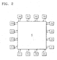
- FIG. 2 schematically illustrates transmitting and receiving data to and from adjacent IPs, based on a code division method.
- FIG. 2 shows a star topology where at least two IPs share one switch.
- 16 IPs IP1, IP2, IP3, ..., IP16 share one switch.
- Each IP is assigned to its own address.
- the assigned IP address and IP( ) will be used with the same meaning throughout the specification.
- Each IP is assigned with an orthogonal code.
- the following ⁇ Table 1> lists IPs and their assigned orthogonal codes.
- Each IP stores the data shown in ⁇ Table 1>.
- the address of an IP generating data to be transferred is called "source address,” and the address of an IP where data is eventually transmitted is called “destination address.”
- source address the address of an IP where data is eventually transmitted
- destination address the address of an IP where data is eventually transmitted.
- the IP(0) spreads the data employing an orthogonal code assigned to the IP(3).
- the IP(0) transfers the spread data to the shared switch "S”.
- the IP(6) spreads the data employing an orthogonal code assigned to the IP(9), and later transfers the spread data to the switch.
- the switch adds the transferred data, and broadcasts them to adjacent IPs. That is, the switch transfers the data being added to IP(0) to IP(15).
- the IP(0) to IP(15) despread the transferred data.
- the IP(3) receives data from the IP(0)
- the IP(9) receives data from the IP(6), respectively. Therefore, the code division method makes it possible for the switch to transmit a lot of data at the same point.
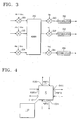
- FIG. 3 illustrates a data switching process based on the code division method.
- FIG. 3 illustrates an NoC constructed of 16 IPs. The NoC based on code division will now explained in detail with reference to FIG. 3 .
- a spreader 300 receives data and an IP for transferring the data.
- the spreader 300 also receives an orthogonal code assigned to the IP for transferring the data.
- the spreader 300 receives an orthogonal code out of w(0) to w(15), which is specially assigned to the IP for transferring the data.
- the spreader 300 spreads the data by using the orthogonal code, and transfers it to an adder 310.
- the other spreaders 302 to 304 also perform the same process as the spreader 300.
- the adder 310 adds the transferred data and transfers them to the despreaders 320 to 324.
- the despreader 320 despreads the transferred data by using its assigned orthogonal code w(0), and transfers it to an accumulator 330.
- the accumulator 330 accumulates the transferred data.
- the despreader 322 despreads the transferred data by using its assigned orthogonal code w(1), and transfers it to an accumulator 332.
- the accumulator 332 accumulates the transferred data.
- the despreader 324 despreads the transferred data by using its assigned orthogonal code w(15), and transfers it to an accumulator 334.
- the accumulator 334 accumulates the transferred data.
- the data is transmitted to the IP that uses the same orthogonal code as the one used by the spreader, and if the IP uses a different orthogonal code from the one used by the spreader, the IP cannot receive the data. This is because of the nature of the orthogonal code having no correlation between codes.
- FIG. 4 illustrates assigning an orthogonal code according to each path, according to an embodiment of the present invention.
- a switch in the net topology-based structure can set a routing path with up to four adjacent switches. Therefore, four orthogonal codes are required for the NoC having the net topology-based structure. At this time, the number of orthogonal codes is maintained constant regardless of the increase in the number of IPs.
- the following ⁇ Table 2> illustrates allocated orthogonal codes per path (direction, output port).
- ⁇ Table 2> Switching direction Allocated orthogonal code Up (North) 0000 Down (South) 0101 Left (West) 0011 Right (East) 0110
- the orthogonal code has ,a fixed length no matter how many IPs exist.
- Each switch included in the NoC stores the same data as shown in the ⁇ Table 2>. Described next is a method for transmitting data from an IP having a source address to an IP having a destination address, on the basis of the ⁇ Table 2>.
- FIG. 5 is a flowchart illustrating the operations conducted by the switch of the present invention. With concurrent reference to FIGS. 4 and 5 , there are four ports, each port with a despreader for despreading data by using its assigned orthogonal code.
- the switch performs operations as follows.
- the switch determines whether there is data to be transmitted at operation S500. If the data to be transmitted has been generated, the switch proceeds with the next operation. However, if the data to be transmitted has not been generated, the switch does not proceed with the next operation but instead repeats operation S500.
- the switch compares the destination address included in the received data with its own address. If it turns out that the destination address is in coincidence with its own address (i.e., the same), the switch proceeds with operation 504, but if the addresses are not coincident with each other, the switch proceeds with operation 506. In operation 504, the switch transfers the transmitted data to an IP connected to the switch.
- the switch calculates a value "a.”
- the "a” can be obtained from the following ⁇ Equation 1>, using source address and "n" values.
- source address the address of an IP connected to the switch conducting the procedure of FIG. 5
- original source address the address of an IP that actually generated data to be transferred
- a source address % n .
- the switch sets a routing path (port) of the data being generated at operation S508. This operation will be explained below in more detail. Then, the switch spreads the data by using an orthogonal code assigned to the port at operation S510. The spread data is transferred to four ports of the switch at operation S512. Each port despreads the transferred data by using its assigned orthogonal code at operation S514. Lastly, each port transfers the despread data to adjacent switches at operation S516.
- the switch includes one spreader and four despreaders. Data spreading is performed by the spreader built in the switch, and data despreading is respectively performed by those four ports disposed outside the switch. Therefore, the switch transmits data to only one port out of the four. That is, only the port using the same orthogonal code with the one used by the spreader transmits the data.
- the data from the port includes information about the original source address and the destination address.
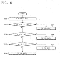
- FIG. 6 illustrates a procedure for setting a routing path of data according to an embodiment of the present invention.
- the switch determines whether a condition b ⁇ (n - a) is satisfied at operation 606. If the condition is satisfied, the switch proceeds with operation 608, but if not, the switch proceeds with operation 610. In operation 608, the switch sets the routing path of data to downward (south). In operation 610, the switch determines whether a condition -a ⁇ b ⁇ -1 is satisfied. If the condition is satisfied, the switch proceeds with operation 612, but if not, the switch proceeds with operation 614. In operation 612, the switch sets the routing path of data to the left side (west). The switch sets the routing path of data to upward (north) at operation 614.
- the switch sets the routing path of data to downward (south). Therefore, the switch spreads the data by using an orthogonal code assigned to the south, and the spread data is transferred to those four ports, respectively. Each port despreads the transmitted data. In this manner, only the port in the south can generate data and transfer the data.
- the switch performs the procedures of FIGS. 5 and 6 on each data. To this end, the switch should spread each data at the same point. This explains why the number of data packets and the number of spreaders should be same. For instance, it is assumed that the routing path of a first data is directed to the east and the routing path of a second data is directed to the south. In this case, the switch spreads the first data by using an orthogonal code assigned to the east, and spreads the second data by using an orthogonal code assigned to the south. The switch then adds the spread data and transfers them to those four ports. Each port despreads the transmitted data, respectively. Performing the despreading process, the port of the east generates the first data, and the port of the south generates the second data. Thusly generated data are transferred to adjacent switches, respectively.
- FIG. 7 illustrates the operation performed by the switch of an embodiment of the present invention.
- the IP performed the data spreading and despreading processes
- the switch performs the data spreading and despreading processes.
- Each port includes an input port and an output port.
- the data input to at least one input port is transferred to a routing path setting unit 700.
- the routing path setting unit 700 receives data from the four input ports, the number of input ports transferred to the routing path setting unit 700 can be varied, depending on the SoC.
- the routing path setting unit 700 uses the destination address included in the transferred data and its own address to determine an output port where the data needs to be transferred. If the destination address and its own address are same, the switch transfers the transferred data to the IP.
- the procedure involved in the determination of the output port by the routing path setting unit 700 is similar to the procedure described referring to FIG. 4 . If an output port 1 is chosen, the routing path setting unit 700 transfers the data to a spreader 710. In such a manner, if an output port 2 is chosen, the routing path setting unit 700 transfers the data to a spreader 712. If an output port 3 is chosen, the routing path setting unit 700 transfers the data to a spreader 714. Lastly, if an output port 4 is chosen, the routing path setting unit 700 transfers the data to a spreader 716.
- the spreader 710 spreads the transferred data by using an orthogonal code w0 and transfers it to the adder 720.
- the spreader 712 spreads the transferred data by using an orthogonal code w1, and transfers it to the adder 720.
- the spreader 714 spreads the transferred data by using an orthogonal code w2, and transfers it to the adder 720.
- spreader 716 spreads the transferred data by using an orthogonal code w3, and transfers it to the adder 720. Then, the adder 720 performs the adding process on the spread data.
- the adder 720 transfers the data to the despreaders 730 to 736, respectively.
- the despreader 730 despreads the transferred data by using the orthogonal code w0, and transfers it to an accumulator 740.
- the despreader 732 despreads the transferred data by using the orthogonal code w1, and transfers it to an accumulator 742.
- the despreader 734 despreads the transferred data by using the orthogonal code w2, and transfers it to an accumulator 744.
- the despreader 736 despreads the transferred data by using the orthogonal code w3, and transfers it to an accumulator 746. After accumulating the data, each of the accumulators 740 to 746 transfers the data to adjacent switches via a corresponding output port.
- Every output port can output data, but only the output port(s) chosen by the routing path setting unit 700 actually outputs data. For example, if the routing path setting unit 700 chooses the output port 0 and the output port 1, only the output ports 0 and 1 output data.
- the code division-based routing setting can be advantageously used for reducing the size of the buffer included in the switch. Moreover, by setting the data routing path by using the orthogonal code, it is possible to shorten transmission time. Therefore, no matter how many IPs are used for constructing the SoC, the orthogonal code can be maintained at constant length.
Landscapes
- Engineering & Computer Science (AREA)
- Computer Networks & Wireless Communication (AREA)
- Signal Processing (AREA)
- Computer Hardware Design (AREA)
- Theoretical Computer Science (AREA)
- Software Systems (AREA)
- Physics & Mathematics (AREA)
- General Engineering & Computer Science (AREA)
- General Physics & Mathematics (AREA)
- Data Exchanges In Wide-Area Networks (AREA)
Claims (4)
- Verfahren zum Einstellen eines Routing-Pfades in einem System on Chip (SoC), wobei das System on Chip mehrere Kerne geistigen Eigentums, die in einer n x n Netztopologie-basierten Struktur (IPO-IP15) angeordnet sind, welche Kerne geistigen Eigentums Module zum Durchführen spezifischer Funktionen sind, welche jeweils einmalige Adressen , aufweisen, und mehrere Schalter (S0-S15) in einer Eins-zu-Eins-Entsprechung mit den Kernen geistigen Eigentums umfasst, wobei das Verfahren zum Übertragen und Empfangen von Daten zwischen den Kernen geistigen Eigentums unter Verwendung von mindestens einem der Schalter dient, wobei die Daten eine Quelladresse des Kernes geistigen Eigentums, wo die Daten erzeugt werden, und eine Zieladresse für die Daten umfassen, dadurch gekennzeichnet, dass das Verfahren Folgendes umfasst:das Zuweisen eines orthogonalen Codes mit gegenseitiger Orthogonalität zu jedem von mehreren Ausgabeanschlüssen für Daten;das Erhalten eines Modulowertes hinsichtlich der Adresse des Schalters durch Verwendung eines Modulo n, der Dimension der Netztopologie, und das Erhalten einer Differenz zwischen der Zieladresse und der Adresse des Schalters;das Festlegen des Ausgabeanschlusses, an welchen die Daten übertragen werden sollen, auf Grundlage des Modulowertes und der Differenz;das Verbreiten der Daten unter Verwendung eines orthogonalen Codes, welcher dem festgelegten Ausgabeanschluss zugewiesen ist;das Übertragen der verbreiteten Daten an die. Ausgabeanschlüsse; unddas Vereinigen der übertragenen Daten unter Verwendung des orthogonalen Codes, welcher jedem Ausgabeanschluss zugewiesen ist.
- Verfahren nach Anspruch 1, wobei die Daten verbreitet werden, wenn die Zieladresse nicht die gleiche ist wie eine Adresse eines Schalters, welcher die Daten empfängt.
- Verfahren nach Anspruch 1, wobei mindestens zweimal Daten an einer Stelle verbreitet werden, und die verbreiteten Daten werden addiert und dann an den Ausgabenanschluss übertragen.
- System on Chip (SoC), umfassend mehrere Kerne geistigen Eigentums, die in einer n x n Netztopologie-basierten Struktur (IP0-IP15) angeordnet sind, welche Kerne geistigen Eigentums Module zum Durchführen spezifischer Funktionen sind, welche jeweils einmalige Adressen aufweisen, und mehrere Schalter (S0-S15) in einer Eins-zu-Eins-Entsprechung mit den Kernen geistigen Eigentums, wobei das System on Chip zum Übertragen und Empfangen von Daten zwischen den Kernen geistigen Eigentums unter Verwendung von mindestens einem der Schalter angeordnet ist, wobei die Daten eine Quelladresse von einem der Kerne geistigen Eigentums, wo die Daten erzeugt werden, und eine Zieladresse der Daten umfassen, dadurch gekennzeichnet, dass die Schalter jeweils Folgendes umfassen:Ausgabeanschlüsse, denen orthogonale Codes mit gegenseitiger Orthogonalität zugewiesen sind;eine Routing-Pfad-Einstelleinheit (700) angeordnet zum:Erhalten eines Modulowertes hinsichtlich der Adresse des Schalters durch Verwendung eines Modulo n, der Dimension der Netztopologie, und Erhalten einer Differenz zwischen der Zieladresse und der Adresse des Schalters; undFestlegen des Ausgabeanschlusses, an welchen die Daten übertragen werden sollen, auf Grundlage des Modulowertes und der Differenz;Verbreiter (710, 712, 714, 716), angeordnet zum Empfangen der Daten und Verbreiten der Daten unter Verwendung des orthogonalen Codes, welcher dem festgelegten Ausgabeanschluss zugewiesen ist;einen Addierer (720), angeordnet zum Addieren von Daten, die von mindestens zwei Verbreitern (710, 712, 714, 716) übertragen wurden, und zum Übertragen der Daten an die Ausgabeanschlüsse; undVereiniger (740, 742, 744, 746) in den Ausgabeanschlüssen, angeordnet zum Vereinigen der übertragenen Daten unter Verwendung der zugewiesenen orthogonalen Codes.
Priority Applications (1)
| Application Number | Priority Date | Filing Date | Title |
|---|---|---|---|
| EP06075944A EP1696336B1 (de) | 2004-02-06 | 2004-12-09 | Vorrichtung und Verfahren zur Einstellung eines Routingpfades zwischen Routern auf einem Chip |
Applications Claiming Priority (2)
| Application Number | Priority Date | Filing Date | Title |
|---|---|---|---|
| KR2004007721 | 2004-02-06 | ||
| KR1020040007721A KR100555753B1 (ko) | 2004-02-06 | 2004-02-06 | 원칩 시스템에서 라우터들간의 라우팅 경로 설정 장치 및방법 |
Related Child Applications (1)
| Application Number | Title | Priority Date | Filing Date |
|---|---|---|---|
| EP06075944A Division EP1696336B1 (de) | 2004-02-06 | 2004-12-09 | Vorrichtung und Verfahren zur Einstellung eines Routingpfades zwischen Routern auf einem Chip |
Publications (3)
| Publication Number | Publication Date |
|---|---|
| EP1562124A2 EP1562124A2 (de) | 2005-08-10 |
| EP1562124A3 EP1562124A3 (de) | 2005-09-14 |
| EP1562124B1 true EP1562124B1 (de) | 2008-02-27 |
Family
ID=34676008
Family Applications (2)
| Application Number | Title | Priority Date | Filing Date |
|---|---|---|---|
| EP04257647A Expired - Lifetime EP1562124B1 (de) | 2004-02-06 | 2004-12-09 | Vorrichtung und Verfahren zum Festlegen eines Routing-Weges zwischen Routern auf einem Chip |
| EP06075944A Expired - Lifetime EP1696336B1 (de) | 2004-02-06 | 2004-12-09 | Vorrichtung und Verfahren zur Einstellung eines Routingpfades zwischen Routern auf einem Chip |
Family Applications After (1)
| Application Number | Title | Priority Date | Filing Date |
|---|---|---|---|
| EP06075944A Expired - Lifetime EP1696336B1 (de) | 2004-02-06 | 2004-12-09 | Vorrichtung und Verfahren zur Einstellung eines Routingpfades zwischen Routern auf einem Chip |
Country Status (4)
| Country | Link |
|---|---|
| US (2) | US7539124B2 (de) |
| EP (2) | EP1562124B1 (de) |
| KR (1) | KR100555753B1 (de) |
| DE (2) | DE602004023323D1 (de) |
Families Citing this family (32)
| Publication number | Priority date | Publication date | Assignee | Title |
|---|---|---|---|---|
| US9143255B2 (en) * | 2002-10-18 | 2015-09-22 | Microsoft Technology Licensing, Llc | Orthogonal signaling for CDMA |
| KR100624641B1 (ko) * | 2004-10-07 | 2006-09-15 | 삼성전자주식회사 | 기능 블록 코어-스위치 포인트 다중 매핑 온 칩 버스 구조및 이를 이용한 반도체 장치 |
| KR100812225B1 (ko) | 2005-12-07 | 2008-03-13 | 한국전자통신연구원 | 멀티프로세서 SoC 플랫폼에 적합한 크로스바 스위치구조 |
| EP1830268B1 (de) * | 2006-03-03 | 2019-05-08 | STMicroelectronics (Research & Development) Limited | Integrierte Mehrzweckschaltung |
| KR100785472B1 (ko) * | 2006-09-19 | 2007-12-13 | 삼성전자주식회사 | 긴급 NoC 패킷 대기시간 관리 장치 및 그 방법 |
| GB0701921D0 (en) * | 2007-02-01 | 2007-03-14 | Univ Edinburgh | Encoding and decoding methods |
| US20090109996A1 (en) * | 2007-10-29 | 2009-04-30 | Hoover Russell D | Network on Chip |
| US20090125706A1 (en) * | 2007-11-08 | 2009-05-14 | Hoover Russell D | Software Pipelining on a Network on Chip |
| US20090125703A1 (en) * | 2007-11-09 | 2009-05-14 | Mejdrich Eric O | Context Switching on a Network On Chip |
| US8261025B2 (en) | 2007-11-12 | 2012-09-04 | International Business Machines Corporation | Software pipelining on a network on chip |
| US8526422B2 (en) * | 2007-11-27 | 2013-09-03 | International Business Machines Corporation | Network on chip with partitions |
| US8473667B2 (en) * | 2008-01-11 | 2013-06-25 | International Business Machines Corporation | Network on chip that maintains cache coherency with invalidation messages |
| US8490110B2 (en) * | 2008-02-15 | 2013-07-16 | International Business Machines Corporation | Network on chip with a low latency, high bandwidth application messaging interconnect |
| US20090260013A1 (en) * | 2008-04-14 | 2009-10-15 | International Business Machines Corporation | Computer Processors With Plural, Pipelined Hardware Threads Of Execution |
| US8423715B2 (en) * | 2008-05-01 | 2013-04-16 | International Business Machines Corporation | Memory management among levels of cache in a memory hierarchy |
| US20090282419A1 (en) * | 2008-05-09 | 2009-11-12 | International Business Machines Corporation | Ordered And Unordered Network-Addressed Message Control With Embedded DMA Commands For A Network On Chip |
| US8494833B2 (en) * | 2008-05-09 | 2013-07-23 | International Business Machines Corporation | Emulating a computer run time environment |
| US8214845B2 (en) * | 2008-05-09 | 2012-07-03 | International Business Machines Corporation | Context switching in a network on chip by thread saving and restoring pointers to memory arrays containing valid message data |
| US20090282211A1 (en) * | 2008-05-09 | 2009-11-12 | International Business Machines | Network On Chip With Partitions |
| US8392664B2 (en) * | 2008-05-09 | 2013-03-05 | International Business Machines Corporation | Network on chip |
| US8040799B2 (en) * | 2008-05-15 | 2011-10-18 | International Business Machines Corporation | Network on chip with minimum guaranteed bandwidth for virtual communications channels |
| US8230179B2 (en) * | 2008-05-15 | 2012-07-24 | International Business Machines Corporation | Administering non-cacheable memory load instructions |
| US8438578B2 (en) * | 2008-06-09 | 2013-05-07 | International Business Machines Corporation | Network on chip with an I/O accelerator |
| US8195884B2 (en) | 2008-09-18 | 2012-06-05 | International Business Machines Corporation | Network on chip with caching restrictions for pages of computer memory |
| US8270316B1 (en) * | 2009-01-30 | 2012-09-18 | The Regents Of The University Of California | On-chip radio frequency (RF) interconnects for network-on-chip designs |
| US8542691B2 (en) * | 2009-06-30 | 2013-09-24 | Oracle International Corporation | Classes of service for network on chips |
| US8639862B2 (en) * | 2009-07-21 | 2014-01-28 | Applied Micro Circuits Corporation | System-on-chip queue status power management |
| US8593960B2 (en) * | 2010-06-30 | 2013-11-26 | Intel Corporation | Providing a bufferless transport method for multi-dimensional mesh topology |
| TWI447728B (zh) * | 2011-03-03 | 2014-08-01 | Mstar Semiconductor Inc | 動態隨機存取記憶體之控制方法及控制器 |
| JP5997359B2 (ja) * | 2012-03-28 | 2016-09-28 | ゼットティーイー コーポレイション | マルチチャネル同期並列伝送の実現方法及びシステム |
| CN107656895B (zh) * | 2017-10-27 | 2023-07-28 | 上海力诺通信科技有限公司 | 一种1u标准高度的正交平台高密度计算架构 |
| GB2586029B (en) * | 2019-07-29 | 2022-07-27 | Siemens Ind Software Inc | Emulating broadcast in a network on chip |
Family Cites Families (14)
| Publication number | Priority date | Publication date | Assignee | Title |
|---|---|---|---|---|
| US4797882A (en) | 1985-10-02 | 1989-01-10 | American Telephone And Telegraph Company, At&T Bell Laboratories | Mesh-based switching network |
| US5896368A (en) * | 1995-05-01 | 1999-04-20 | Telefonaktiebolaget Lm Ericsson | Multi-code compressed mode DS-CDMA systems and methods |
| US6307868B1 (en) * | 1995-08-25 | 2001-10-23 | Terayon Communication Systems, Inc. | Apparatus and method for SCDMA digital data transmission using orthogonal codes and a head end modem with no tracking loops |
| JPH11150523A (ja) * | 1997-11-17 | 1999-06-02 | Oki Electric Ind Co Ltd | スペクトラム拡散送信装置、スペクトラム拡散受信装置及びスペクトラム拡散通信システム |
| US6741552B1 (en) | 1998-02-12 | 2004-05-25 | Pmc Sierra Inertnational, Inc. | Fault-tolerant, highly-scalable cell switching architecture |
| US6700881B1 (en) * | 1998-03-02 | 2004-03-02 | Samsung Electronics Co., Ltd. | Rate control device and method for CDMA communication system |
| US6377607B1 (en) * | 1999-05-13 | 2002-04-23 | Qualcomm Incorporated | System and method for performing accurate demodulation of turbo-encoded signals via pilot assisted coherent demodulation |
| US6912196B1 (en) * | 2000-05-15 | 2005-06-28 | Dunti, Llc | Communication network and protocol which can efficiently maintain transmission across a disrupted network |
| JP4187377B2 (ja) * | 2000-02-23 | 2008-11-26 | 富士通株式会社 | 無線送受信機及び電波放射方向制御方法 |
| JP5079189B2 (ja) * | 2001-04-13 | 2012-11-21 | Kddi株式会社 | 多ビームセルラ無線基地局、移動機及びスペクトラム拡散信号送信方法 |
| JP4092291B2 (ja) * | 2001-08-02 | 2008-05-28 | インフィネオン テヒノロジース アクチェンゲゼルシャフト | 構成可能なターミナル・エンジン |
| US7280752B2 (en) * | 2002-02-22 | 2007-10-09 | Intel Corporation | Network address routing using multiple routing identifiers |
| US20060095626A1 (en) * | 2004-10-28 | 2006-05-04 | Abocom Systems, Inc. | Multifunction adapter |
| KR100594943B1 (ko) * | 2004-11-30 | 2006-06-30 | 리전츠 오브 더 유니버스티 오브 미네소타 | 원칩시스템에서 데이터 변복조 방법 |
-
2004
- 2004-02-06 KR KR1020040007721A patent/KR100555753B1/ko not_active Expired - Lifetime
- 2004-11-30 US US10/998,571 patent/US7539124B2/en active Active
- 2004-12-09 EP EP04257647A patent/EP1562124B1/de not_active Expired - Lifetime
- 2004-12-09 DE DE602004023323T patent/DE602004023323D1/de not_active Expired - Lifetime
- 2004-12-09 DE DE602004012061T patent/DE602004012061T2/de not_active Expired - Lifetime
- 2004-12-09 EP EP06075944A patent/EP1696336B1/de not_active Expired - Lifetime
-
2009
- 2009-04-14 US US12/385,622 patent/US20090201925A1/en not_active Abandoned
Also Published As
| Publication number | Publication date |
|---|---|
| DE602004023323D1 (de) | 2009-11-05 |
| US20050185642A1 (en) | 2005-08-25 |
| EP1696336B1 (de) | 2009-09-23 |
| EP1696336A2 (de) | 2006-08-30 |
| KR20050079458A (ko) | 2005-08-10 |
| EP1696336A3 (de) | 2006-09-20 |
| EP1562124A3 (de) | 2005-09-14 |
| EP1562124A2 (de) | 2005-08-10 |
| US20090201925A1 (en) | 2009-08-13 |
| KR100555753B1 (ko) | 2006-03-03 |
| US7539124B2 (en) | 2009-05-26 |
| DE602004012061D1 (de) | 2008-04-10 |
| DE602004012061T2 (de) | 2008-06-12 |
Similar Documents
| Publication | Publication Date | Title |
|---|---|---|
| EP1696336B1 (de) | Vorrichtung und Verfahren zur Einstellung eines Routingpfades zwischen Routern auf einem Chip | |
| Giacopelli et al. | Sunshine: A high performance self-routing broadband packet switch architecture | |
| EP1560376B1 (de) | System-on-chip zum Pfadaufbau zwischen Routern und Verfahren dazu | |
| Moraes et al. | HERMES: an infrastructure for low area overhead packet-switching networks on chip | |
| Leroy et al. | Spatial division multiplexing: a novel approach for guaranteed throughput on NoCs | |
| EP2664108B1 (de) | Asymmetrische ringtopologie für reduzierte latenzzeit in on-chip-ringnetzwerken | |
| CN103684961A (zh) | 自动构建无死锁互连 | |
| Moraes et al. | A Low Area Overhead Packet-switched Network on Chip: Architecture and Prototyping. | |
| EP1744497B1 (de) | Verfahren zum Verwalten einer Vielzahl von virtuellen Verbindungen zur gemeinsamen Nutzung auf einer Verbindungsleitung und Netzwerk zur Implementierung dieses Verfahrens | |
| Seifi et al. | A clustered NoC in group communication | |
| KR100682060B1 (ko) | 네트워크 온칩 시스템의 스위칭 장치 및 그의 스케쥴링방법 | |
| Wu et al. | Design of a high-performance switch for circuit-switched on-chip networks | |
| Lusala et al. | A SDM-TDM based circuit-switched router for on-chip networks | |
| Ejaz et al. | Costs and benefits of flexibility in spatial division circuit switched networks-on-chip | |
| Poovendran et al. | On Chip Implementation of Packet Switched Network | |
| Lusala et al. | Combining circuit and packet switching with bus architecture in a NoC for real-time applications | |
| de Lima et al. | FlexOE: a congestion-aware routing algorithm for NoCs | |
| Khan | Performance analysis of XY routing algorithm using 2-D mesh (M x N) topology | |
| Lusala et al. | A hybrid router combining circuit switching and packet switching with bus architecture for on-chip networks | |
| Achar et al. | FPGA based Design and Simulation of basic Routing Protocols | |
| Lusala et al. | A SDM-TDM-based circuit-switched router for on-chip networks | |
| Lusala et al. | A hybrid NoC combining SDM-based circuit switching with packet switching for real-time applications | |
| Chi et al. | Efficient switches for network-on-chip based embedded systems | |
| Ayyad | The Penta-S: A Scalable Crossbar Network for Distributed Shared Memory Multiprocessor Systems | |
| Sathe et al. | Design of a guaranteed throughput router for on-chip networks |
Legal Events
| Date | Code | Title | Description |
|---|---|---|---|
| PUAI | Public reference made under article 153(3) epc to a published international application that has entered the european phase |
Free format text: ORIGINAL CODE: 0009012 |
|
| PUAL | Search report despatched |
Free format text: ORIGINAL CODE: 0009013 |
|
| AK | Designated contracting states |
Kind code of ref document: A2 Designated state(s): AT BE BG CH CY CZ DE DK EE ES FI FR GB GR HU IE IS IT LI LT LU MC NL PL PT RO SE SI SK TR |
|
| AX | Request for extension of the european patent |
Extension state: AL BA HR LV MK YU |
|
| AK | Designated contracting states |
Kind code of ref document: A3 Designated state(s): AT BE BG CH CY CZ DE DK EE ES FI FR GB GR HU IE IS IT LI LT LU MC NL PL PT RO SE SI SK TR |
|
| AX | Request for extension of the european patent |
Extension state: AL BA HR LV MK YU |
|
| 17P | Request for examination filed |
Effective date: 20060104 |
|
| AKX | Designation fees paid |
Designated state(s): DE FI FR SE |
|
| 17Q | First examination report despatched |
Effective date: 20060208 |
|
| GRAP | Despatch of communication of intention to grant a patent |
Free format text: ORIGINAL CODE: EPIDOSNIGR1 |
|
| RIN1 | Information on inventor provided before grant (corrected) |
Inventor name: LEE, BEAM-HAK Inventor name: RHIM, SANG-WOO Inventor name: KIM, EUI-SEOK,207-701, SAMSUNG APT. Inventor name: LEE, JAE-KON,108-808, DONGSUWON LG VILLAGE |
|
| GRAS | Grant fee paid |
Free format text: ORIGINAL CODE: EPIDOSNIGR3 |
|
| GRAA | (expected) grant |
Free format text: ORIGINAL CODE: 0009210 |
|
| AK | Designated contracting states |
Kind code of ref document: B1 Designated state(s): DE FI FR SE |
|
| REF | Corresponds to: |
Ref document number: 602004012061 Country of ref document: DE Date of ref document: 20080410 Kind code of ref document: P |
|
| REG | Reference to a national code |
Ref country code: SE Ref legal event code: TRGR |
|
| ET | Fr: translation filed | ||
| PLBE | No opposition filed within time limit |
Free format text: ORIGINAL CODE: 0009261 |
|
| STAA | Information on the status of an ep patent application or granted ep patent |
Free format text: STATUS: NO OPPOSITION FILED WITHIN TIME LIMIT |
|
| 26N | No opposition filed |
Effective date: 20081128 |
|
| REG | Reference to a national code |
Ref country code: FR Ref legal event code: PLFP Year of fee payment: 12 |
|
| REG | Reference to a national code |
Ref country code: FR Ref legal event code: PLFP Year of fee payment: 13 |
|
| REG | Reference to a national code |
Ref country code: FR Ref legal event code: PLFP Year of fee payment: 14 |
|
| P01 | Opt-out of the competence of the unified patent court (upc) registered |
Effective date: 20230520 |
|
| PGFP | Annual fee paid to national office [announced via postgrant information from national office to epo] |
Ref country code: SE Payment date: 20231026 Year of fee payment: 20 Ref country code: FR Payment date: 20231024 Year of fee payment: 20 Ref country code: FI Payment date: 20231218 Year of fee payment: 20 Ref country code: DE Payment date: 20231024 Year of fee payment: 20 |
|
| REG | Reference to a national code |
Ref country code: DE Ref legal event code: R071 Ref document number: 602004012061 Country of ref document: DE |
|
| REG | Reference to a national code |
Ref country code: SE Ref legal event code: EUG |