EP1561794A1 - Material for organic electroluminescent device and organic electroluminescent device using same - Google Patents
Material for organic electroluminescent device and organic electroluminescent device using same Download PDFInfo
- Publication number
- EP1561794A1 EP1561794A1 EP03754188A EP03754188A EP1561794A1 EP 1561794 A1 EP1561794 A1 EP 1561794A1 EP 03754188 A EP03754188 A EP 03754188A EP 03754188 A EP03754188 A EP 03754188A EP 1561794 A1 EP1561794 A1 EP 1561794A1
- Authority
- EP
- European Patent Office
- Prior art keywords
- electroluminescent device
- light
- organic electroluminescent
- organic
- substituted
- Prior art date
- Legal status (The legal status is an assumption and is not a legal conclusion. Google has not performed a legal analysis and makes no representation as to the accuracy of the status listed.)
- Granted
Links
Images






Classifications
-
- H—ELECTRICITY
- H05—ELECTRIC TECHNIQUES NOT OTHERWISE PROVIDED FOR
- H05B—ELECTRIC HEATING; ELECTRIC LIGHT SOURCES NOT OTHERWISE PROVIDED FOR; CIRCUIT ARRANGEMENTS FOR ELECTRIC LIGHT SOURCES, IN GENERAL
- H05B33/00—Electroluminescent light sources
- H05B33/12—Light sources with substantially two-dimensional [2D] radiating surfaces
- H05B33/14—Light sources with substantially two-dimensional [2D] radiating surfaces characterised by the chemical or physical composition or the arrangement of the electroluminescent material, or by the simultaneous addition of the electroluminescent material in or onto the light source
-
- C—CHEMISTRY; METALLURGY
- C09—DYES; PAINTS; POLISHES; NATURAL RESINS; ADHESIVES; COMPOSITIONS NOT OTHERWISE PROVIDED FOR; APPLICATIONS OF MATERIALS NOT OTHERWISE PROVIDED FOR
- C09K—MATERIALS FOR MISCELLANEOUS APPLICATIONS, NOT PROVIDED FOR ELSEWHERE
- C09K11/00—Luminescent materials, e.g. electroluminescent or chemiluminescent
- C09K11/06—Luminescent materials, e.g. electroluminescent or chemiluminescent containing organic luminescent materials
-
- H—ELECTRICITY
- H10—SEMICONDUCTOR DEVICES; ELECTRIC SOLID-STATE DEVICES NOT OTHERWISE PROVIDED FOR
- H10K—ORGANIC ELECTRIC SOLID-STATE DEVICES
- H10K85/00—Organic materials used in the body or electrodes of devices covered by this subclass
- H10K85/60—Organic compounds having low molecular weight
- H10K85/615—Polycyclic condensed aromatic hydrocarbons, e.g. anthracene
- H10K85/622—Polycyclic condensed aromatic hydrocarbons, e.g. anthracene containing four rings, e.g. pyrene
-
- H—ELECTRICITY
- H10—SEMICONDUCTOR DEVICES; ELECTRIC SOLID-STATE DEVICES NOT OTHERWISE PROVIDED FOR
- H10K—ORGANIC ELECTRIC SOLID-STATE DEVICES
- H10K85/00—Organic materials used in the body or electrodes of devices covered by this subclass
- H10K85/60—Organic compounds having low molecular weight
- H10K85/631—Amine compounds having at least two aryl rest on at least one amine-nitrogen atom, e.g. triphenylamine
- H10K85/633—Amine compounds having at least two aryl rest on at least one amine-nitrogen atom, e.g. triphenylamine comprising polycyclic condensed aromatic hydrocarbons as substituents on the nitrogen atom
-
- H—ELECTRICITY
- H10—SEMICONDUCTOR DEVICES; ELECTRIC SOLID-STATE DEVICES NOT OTHERWISE PROVIDED FOR
- H10K—ORGANIC ELECTRIC SOLID-STATE DEVICES
- H10K85/00—Organic materials used in the body or electrodes of devices covered by this subclass
- H10K85/60—Organic compounds having low molecular weight
- H10K85/649—Aromatic compounds comprising a hetero atom
- H10K85/657—Polycyclic condensed heteroaromatic hydrocarbons
-
- C—CHEMISTRY; METALLURGY
- C09—DYES; PAINTS; POLISHES; NATURAL RESINS; ADHESIVES; COMPOSITIONS NOT OTHERWISE PROVIDED FOR; APPLICATIONS OF MATERIALS NOT OTHERWISE PROVIDED FOR
- C09K—MATERIALS FOR MISCELLANEOUS APPLICATIONS, NOT PROVIDED FOR ELSEWHERE
- C09K2211/00—Chemical nature of organic luminescent or tenebrescent compounds
- C09K2211/10—Non-macromolecular compounds
- C09K2211/1003—Carbocyclic compounds
- C09K2211/1011—Condensed systems
-
- C—CHEMISTRY; METALLURGY
- C09—DYES; PAINTS; POLISHES; NATURAL RESINS; ADHESIVES; COMPOSITIONS NOT OTHERWISE PROVIDED FOR; APPLICATIONS OF MATERIALS NOT OTHERWISE PROVIDED FOR
- C09K—MATERIALS FOR MISCELLANEOUS APPLICATIONS, NOT PROVIDED FOR ELSEWHERE
- C09K2211/00—Chemical nature of organic luminescent or tenebrescent compounds
- C09K2211/10—Non-macromolecular compounds
- C09K2211/1003—Carbocyclic compounds
- C09K2211/1014—Carbocyclic compounds bridged by heteroatoms, e.g. N, P, Si or B
-
- H—ELECTRICITY
- H10—SEMICONDUCTOR DEVICES; ELECTRIC SOLID-STATE DEVICES NOT OTHERWISE PROVIDED FOR
- H10K—ORGANIC ELECTRIC SOLID-STATE DEVICES
- H10K50/00—Organic light-emitting devices
- H10K50/10—OLEDs or polymer light-emitting diodes [PLED]
- H10K50/11—OLEDs or polymer light-emitting diodes [PLED] characterised by the electroluminescent [EL] layers
-
- H—ELECTRICITY
- H10—SEMICONDUCTOR DEVICES; ELECTRIC SOLID-STATE DEVICES NOT OTHERWISE PROVIDED FOR
- H10K—ORGANIC ELECTRIC SOLID-STATE DEVICES
- H10K85/00—Organic materials used in the body or electrodes of devices covered by this subclass
- H10K85/60—Organic compounds having low molecular weight
- H10K85/615—Polycyclic condensed aromatic hydrocarbons, e.g. anthracene
- H10K85/626—Polycyclic condensed aromatic hydrocarbons, e.g. anthracene containing more than one polycyclic condensed aromatic rings, e.g. bis-anthracene
-
- Y—GENERAL TAGGING OF NEW TECHNOLOGICAL DEVELOPMENTS; GENERAL TAGGING OF CROSS-SECTIONAL TECHNOLOGIES SPANNING OVER SEVERAL SECTIONS OF THE IPC; TECHNICAL SUBJECTS COVERED BY FORMER USPC CROSS-REFERENCE ART COLLECTIONS [XRACs] AND DIGESTS
- Y10—TECHNICAL SUBJECTS COVERED BY FORMER USPC
- Y10S—TECHNICAL SUBJECTS COVERED BY FORMER USPC CROSS-REFERENCE ART COLLECTIONS [XRACs] AND DIGESTS
- Y10S428/00—Stock material or miscellaneous articles
- Y10S428/917—Electroluminescent
Definitions
- the present invention relates to a material for use in an organic electroluminescent device (hereinafter may be referred to as "organic electroluminescent device material”) which is employed as a flat light-emitting device for use in a wall-mounted, flat-panel television set or as a light source such as a backside light of a display device; which has a long service life; and which can emit blue light of high color purity at high emission efficiency.
- organic electroluminescent device material which is employed as a flat light-emitting device for use in a wall-mounted, flat-panel television set or as a light source such as a backside light of a display device; which has a long service life; and which can emit blue light of high color purity at high emission efficiency.
- organic electroluminescent device material which is employed as a flat light-emitting device for use in a wall-mounted, flat-panel television set or as a light source such as a backside light of a display device; which has a long service life; and which can emit blue
- Electroluminescent (EL) devices including an organic substance have been promising candidates for wide-area, full-color, and inexpensive display devices based on solid-state emission, and development of a variety of such devices is under way.
- an EL device is composed of a pair of electrodes, and a light-emitting layer interposed between the electrodes.
- Light emission is a phenomenon occurring through the following mechanism. When an electric field is applied between electrodes, electrons are injected from the cathode and holes are injected from the anode, both to the light-emitting layer. In the light-emitting layer, the injected electrons are recombined with holes, thereby creating an excited state. During transition from the excited state to the ground state, energy is released as light.
- organic EL devices As compared with inorganic light-emitting diodes, conventional organic EL devices are operated at higher operation voltage and exhibit lower emission luminance and emission efficiency. In addition, organic EL devices are not actually used in practice, because of considerable impairment in characteristics. Recently, organic EL devices have been improved step by step. However, further improvement in emission efficiency and service life is demanded.
- One disclosed technique is based on employment of a single monoanthracene compound serving as an organic light-emitting material (Japanese Patent Application Laid-Open ( kokai ) No. 11-3782). However, this technique is not practically employed, since luminance at a current density of 165 mA/cm 2 is as low as 1,650 cd/m 2 , and emission efficiency is as considerably low as 1 cd/A.
- Another disclosed technique is based on employment of a single bisanthracene compound serving as an organic light-emitting material (Japanese Patent Application Laid-Open ( k okai) No. 8-12600).
- emission efficiency attained by the technique is as low as about 1 to 3 cd/A, which remains to be improved before the technique is put into practice.
- a long-life organic EL device has been proposed (WO 94/06157).
- the EL device includes a distyryl compound serving as an organic light-emitting material in combination with an additive such as styrylamine.
- the proposed EL device has an insufficient half-life, which is to be further improved.
- Still another disclosed technique is based on employment of an organic light-emitting medium layer containing a mono- or a bis-anthracene compound and a distyryl compound (Japanese Patent Application Laid-Open ( kokai ) No. 2001-284050). According to the technique, a peak in an emission spectrum is red-shifted because of a conjugation structure of the styryl compound, thereby impairing color purity.
- an object of the present invention is to provide a material for use in an organic EL device material which has a long service life and which can emit blue light of high color purity at high emission efficiency.
- Another object of the invention is to provide an organic EL device including the material.
- the present inventors have carried out extensive studies with an aim toward developing a material for use in an organic EL device exhibiting the aforementioned desirable properties and an organic EL device including the material, and have found that the aforementioned objects can be attained through employment of an aromatic amine derivative in which amine moieties are linked to a chrysene moiety and which is represented by any of the following formulas (I) to (IV).
- the present invention has been accomplished on the basis of this finding.
- the present invention provides an organic EL device material comprising an aromatic amine derivative represented by any of the following formulas (I) to (IV): (wherein each of A 1 to A 12 represents a hydrogen atom, a substituted or unsubstituted alkyl group having 1 to 50 carbon atoms, a substituted or unsubstituted aryl group having 5 to 50 ring carbon atoms, a substituted or unsubstituted cycloalkyl group having 3 to 50 ring carbon atoms, a substituted or unsubstituted alkoxyl group having 1 to 50 carbon atoms, a substituted or unsubstituted aryloxy group having 5 to 50 ring carbon atoms, a substituted or unsubstituted arylamino group having 5 to 50 ring carbon atoms, a substituted or unsubstituted alkylamino group having 1 to 20 carbon atoms, or a halogen atom; m is an integer of 0
- the present invention also provides an organic EL device comprising a cathode, an anode, and one or more organic thin-film layers interposed between the cathode and the anode, the organic thin-layers including at least a light-emitting layer, wherein at least one of the organic thin-film layers contains the organic EL device material in the form of single component material or a mixture of a plurality of components.
- the present invention also provides such an organic EL device, wherein the light-emitting layer contains the organic EL device material in an amount of 0.1 to 20 wt.%.
- the organic EL device material of the present invention comprises an aromatic amine derivative represented by any of the aforementioned formulas (I) to (IV).
- each of A 1 to A 12 represents a hydrogen atom, a substituted or unsubstituted alkyl group having 1 to 50 (preferably 1 to 20) carbon atoms, a substituted or unsubstituted aryl group having 5 to 50 (preferably 5 to 20) ring carbon atoms, a substituted or unsubstituted cycloalkyl group having 3 to 50 (preferably 5 to 12) ring carbon atoms, a substituted or unsubstituted alkoxyl group having 1 to 50 (preferably 1 to 6) carbon atoms, a substituted or unsubstituted aryloxy group having 5 to 50 (preferably 5 to 18) ring carbon atoms, a substituted or unsubstituted arylamino group having 5 to 50 (preferably 5 to 18) ring carbon atoms, a substituted or unsubstituted alkylamino group having 1 to 20 carbon atoms (preferably 1 to 6), or a hal
- Examples of the substituted or unsubstituted alkyl group represented by any of A 1 to A 12 include methyl, ethyl, propyl, isopropyl, butyl, sec-butyl, tert-butyl, pentyl, hexyl, heptyl, octyl, stearyl, 2-phenylisopropyl, trichloromethyl, trifluoromethyl, benzyl, ⁇ -phenoxybenzyl, ⁇ , ⁇ -dimethylbenzyl, ⁇ , ⁇ -methylphenylbenzyl, ⁇ , ⁇ -ditrifluoromethylbenzyl, triphenylmethyl, and ⁇ -benzyloxybenzyl.
- Examples of the substituted or unsubstituted aryl group represented by any of A 1 to A 12 include phenyl, 2-methylphenyl, 3-methylphenyl, 4-methylphenyl, 4-ethylphenyl, biphenyl, 4-methylbiphenyl, 4-ethylbiphenyl, 4-cyclohexylbiphenyl, terphenyl, 3,5-dichlorophenyl, naphthyl, 5-methylnaphthyl, anthryl, and pyrenyl.
- Examples of the substituted or unsubstituted cycloalkyl group represented by any of A 1 to A 12 include cyclopropyl, cyclobutyl, cyclopentyl, and cyclohexyl.
- Examples of the substituted or unsubstituted alkoxyl group represented by any of A 1 to A 12 include methoxy, ethoxy, propoxy, isopropoxy, butoxy, isobotoxy, sec-butoxy, tert-butoxy, pentyloxy groups, and hexyloxy groups.
- Examples of the substituted or unsubstituted aryloxy group represented by any of A 1 to A 12 include phenoxy, tolyloxy, and naphthyloxy.
- Examples of the substituted or unsubstituted arylamino group represented by any of A 1 to A 12 include diphenylamino, ditolylamino, dinaphthylamino, and naphthylphenylamino.
- Examples of the substituted or unsubstituted alkylamino group represented by any of A 1 to A 12 include dimethylamino, diethylamino, and dihexylamino.
- Examples of the halogen atom represented by any of A 1 to A 12 include fluorine, chlorine, and bromine.
- At least one of A 1 to A 4 does not represent a hydrogen atom.
- at least one of A 5 to A 8 does not represent a hydrogen atom.
- at least one of A 9 and A 10 does not represent a hydrogen atom.
- at least one of A 11 and A 12 does not represent a hydrogen atom.
- the "m” is an integer of 0 to 5, preferably 0 to 2.
- groups represented by any of A 1 to A 12 may be identical to or different from one another, or may be linked together to form a saturated or unsaturated ring.
- Each pair of A 1 and A 2 , A 3 and A 4 , A 5 and A 6 , A 7 and A 8 , A 9 and A 10 , and A 11 and A 12 is such that the members thereof may be linked together to form a saturated or unsaturated ring.
- Each of R 1 to R 42 represents a hydrogen atom, a substituted or unsubstituted alkyl group having 1 to 20 ring carbon atoms, a substituted or unsubstituted aryl group having 6 to 20 ring carbon atoms, or a cyano group.
- Examples of the substituted or unsubstituted alkyl group and aryl group represented by any of R 1 to R 42 include the same groups as mentioned in relation to the A 1 to A 12 .
- Each of X 1 to X 3 represents a substituted or unsubstituted arylene group having 6 to 20 ring carbon atoms.
- Examples of the substituted or unsubstituted arylene group represented by any of X 1 to X 3 include phenyl, biphenyl, terphenyl, divalent groups derived from naphthalene, fluorene, or a similar compound, and divalent groups formed by linking a plurality of the compounds.
- aromatic amine derivative represented by any of formulas (I) to (IV) include, but are not limited to, the following.
- the symbol "Me” denotes a methyl group.
- the compound of the present invention represented by any of the formulas (I) to (IV) has a structure in which amine moieties substituted by a substituent-containing benzene ring are linked to a chrysene moiety. Therefore, association of molecules of the compound is prevented, thereby prolonging the life time.
- the compound of the present invention exhibits highly fluorescent properties in the solid state and excellent electric-field-induced emission characteristics, and attains a fluorescence quantum efficiency of 0.3 or more.
- the compound exhibits excellent hole-injectability and hole-transportability from a metallic electrode or an organic thin-film layer, as well as excellent electron-injectability and electron-transportability from a metallic electrode or an organic thin-film layer.
- the compound of the present invention is effectively used as an organic EL device material.
- the compound may be used in combination with another hole-transporting material, another electron-transporting material, or a doping material.
- the organic EL device of the present invention is composed of a cathode, an anode, and one or more organic thin films interposed between the cathode and the anode.
- a light-emitting layer is interposed between the cathode and the anode.
- the light-emitting layer contains a light-emitting material and may further contain a hole-injecting material for transporting, to the light-emitting material, holes injected from the anode, or an electron-injecting material for transporting, to the light-emitting material, electrons injected from the cathode.
- the compound represented by any of formulas (I) to (IV) can be used as a light-emitting material in the light-emitting layer.
- the light-emitting layer preferably contains the organic EL device material in an amount of 0.1 to 20 wt.%, more preferably 1 to 10 wt.%. Since the organic EL device material exhibits remarkably high fluorescence quantum efficiency and high hole- and electron-transportability and can provide uniform thin film, the light-emitting layer can be formed solely from the light-emitting material of the present invention.
- Examples of the multi-layer structure of the organic EL device include (anode/hole-injecting layer/light-emitting layer/cathode), (anode/light-emitting layer/electron-injecting layer/cathode), and (anode/hole-injecting layer/light-emitting layer/electron-injecting layer/cathode).
- the light-emitting layer may further contain, in accordance with needs, a known light-emitting material, doping material, hole-injecting material, or electron-injecting material.
- a known light-emitting material When the organic EL device has a multi-layer structure, decrease in luminance and life time due to quenching can be prevented.
- a light-emitting material can be used in combination with a doping material, a hole-injecting material, or an electron-injecting material.
- emission luminance and emission efficiency can be elevated, and red-light-emission or blue-light-emission can be attained.
- Each of the hole-injecting layer, light-emitting layer, and electron-injecting layer may be composed of two or more layers.
- a layer to which holes are injected from an electrode is referred to as "hole-injecting layer”
- a layer for receiving holes from the hole-injecting layer and transporting the holes to the light-emitting layer is referred to as "hole-transporting layer.”
- electron-injecting layer a layer to which electrons are injected from an electrode
- electron-transporting layer a layer to which electrons are injected from an electrode
- a layer for receiving electrons from the electron-injecting layer and transporting the electrons to the light-emitting layer is referred to as "electron-transporting layer.”
- These layers may be employed in accordance with energy level of the material, heat resistance, adhesion with respect to an organic layer or a metallic electrode, or other factors.
- the light-emitting material or the doping material which may be used in the light-emitting layer in combination with the compound represented by any of formulas (I) to (IV).
- Examples include anthracene, naphthalene, phenanthrene, pyrene, tetracene, coronene, chrysene, fluoresceine, perylene, phthaloperylene, naphthaloperylene, perynone, phthaloperynone, naphthaloperynone, diphenylbutadiene, tetraphenylbutadiene, coumarin, oxadiazole, aldazine, bisbenzoxazoline, bisstyryl, pyrazine, cyclopentadiene, quinoline metal complexes, aminoquinoline metal complexes, benzoquinoline metal complexes, imines, diphenylethylene, vinylanthracene, diaminocarbazole,
- the hole-injecting material is a compound which can transfer holes, which exhibits hole-injecting effect (from an anode) and excellent hole-injecting effect to a light-emitting layer or a light-emitting material, which prevents transfer of excitons generated in the light-emitting layer to an electron-injecting layer or an electron-injecting material, and which has excellent thin-film-formability.
- hole-injecting material No particular limitation is imposed on the hole-injecting material, and specific examples include phthalocyanine derivatives, naphthalocyanine derivatives, porphyrin derivatives, oxazole, oxadiazole, triazole, imidazole, imidazolone, imidazolethione, pyrazoline, pyrazolone, tetrahydroimidazole, oxazole, oxadiazole, hydrazone, acylhydrazone, polyarylalkanes, stilbene, butadiene, benzidine-type triphenylamines, styrylamine-type triphenylamines, diamine-type triphenylamines, derivatives thereof, and polymer materials such as polyvinylcarbazole, polysilane, and conductive polymers.
- an aromatic tertiary amine derivative and a phthalocyanine derivative serve as a more effective hole-injecting material.
- aromatic tertiary amine derivative No particular limitation is imposed on the type of the aromatic tertiary amine derivative, and examples include triphenylamine, tritolylamine, tolyldiphenylamine, N,N'-diphenyl-N,N'-(3-methylphenyl)-1,1'-biphenyl-4,4'-diamine, N,N,N',N'-(4-methylphenyl)-1,1'-phenyl-4,4'-diamine, N,N,N',N'-(4-methylphenyl)-1,1'-biphenyl-4,4'-diamine, N,N'-diphenyl-N,N'-dinaphthyl-1,1'-biphenyl-4,4'-diamine, N,N'-(methylphenyl)-N,N'-(4-n-butylphenyl)-phenanthrene-9,10-diamine, N,N
- phthalocyanine (Pc) derivative examples include phthalocyanine derivatives such as H 2 Pc, CuPc, CoPc, NiPc, ZnPc, PdPc, FePc, MnPc, ClAlPc, ClGaPc, ClInPc, ClSnPc, Cl 2 SiPc, (HO)AlPc, (HO)GaPc, VOPc, TiOPc, MoOPc, GaPc-O-GaPc, and naphthalocyanine derivatives.
- phthalocyanine derivatives such as H 2 Pc, CuPc, CoPc, NiPc, ZnPc, PdPc, FePc, MnPc, ClAlPc, ClGaPc, ClInPc, ClSnPc, Cl 2 SiPc, (HO)AlPc, (HO)GaPc, VOPc, TiOPc, MoOPc, GaPc-O-GaPc, and n
- the organic EL device of the present invention preferably includes, between the light-emitting layer and the anode, a layer containing any of these aromatic tertiary amine derivatives and/or phthalocyanine derivatives, for example, the aforementioned hole-transporting layer or a hole-injecting layer.
- the electron-injecting material is a compound which can transfer electrons, which exhibits electron-injecting effect (from a cathode) and excellent electron-injecting effect to a light-emitting layer or a light-emitting material, which prevents transfer of excitons generated in the light-emitting layer to a hole-injecting layer, and which has excellent thin-film-formability.
- the electron-injecting material No particular limitation is imposed on the electron-injecting material, and specific examples include fluorenone, anthraquinodimethane, diphenoquinone, thiopyrane dioxide, oxazole, oxadiazole, triazole, imidazole, perylenetetracarboxylic acid, fluorenylidenemethane, anthraquinodimethane, anthrone, and derivatives thereof.
- the hole-injecting material may be sensitized through addition of an electron-acceptor thereto, and the electron-injecting material may be sensitized through addition of an electron-donor thereto.
- a metal complex compound and a nitrogen-containing five-membered ring derivative serve as a more effective electron-injecting material.
- the nitrogen-containing five-membered-ring derivative is preferably an oxazole derivative, a thiazole derivative, an oxadiazole derivative, a thiadiazole derivative, and a triazole derivative.
- the derivative include 2,5-bis(1-phenyl)-1,3,4-oxazole, dimethyl-POPOP, 2,5-bis (1-phenyl)-1,3,4-thiazole, 2,5-bis (1-phenyl)-1,3,4-oxadiazole, 2-(4'-tert-butylphenyl)-5-(4''-biphenyl)-1,3,4-oxadiazole, 2,5-bis(1-naphthyl)-1,3,4-oxadiazole, 1,4-bis[2-(5-phenyloxadiazolyl)]benzene, 1,4-bis[2-(5-phenyloxadiazolyl)-4-tert-butylbenzene], 2-(4'-tert-
- the light-emitting layer may contain, in addition to the compound represented by any of formulas (I) to (IV), at least one species selected from among a light-emitting material, a doping material, a hole-injecting material, and an electron-injecting material.
- the surface of the device may be coated with a protective layer.
- the entirety of the device may be protected with silicone oil, resin, or a similar material.
- the anode included in the organic EL device of the present invention is preferably formed of a conductive material having a work function higher than 4 eV.
- the conductive material include carbon, aluminum, vanadium, iron, cobalt, nickel, tungsten, silver, gold, platinum, palladium, alloys thereof, metal oxides such as tin oxide and indium oxide used in an ITO substrate or an NESA substrate, and organic conductive resins such as polythiophene and polypyrrole.
- the cathode included in the organic EL device of the present invention is preferably formed of a conductive material having a work function lower than 4 eV.
- the conductive material examples include magnesium, calcium, tin, lead, titanium, yttrium, lithium, ruthenium, manganese, aluminum, lithium fluoride, and alloys thereof.
- the type of alloys and typical examples of the alloys include magnesium/silver, magnesium/indium, and lithium/aluminum.
- the alloy composition is appropriately regulated in accordance with temperature of vapor-deposition sources, atmosphere, vacuum degree, or other factors.
- each of the anode and the cathode may be composed of two or more layers.
- At least one surface of the device is preferably transparent sufficiently in a wavelength region of the emitted light.
- the substrate is also transparent.
- Such a transparent electrode is produced from the aforementioned conductive material through vapor deposition, sputtering, or a similar method, such that a predetermined transparency is ensured.
- the light-emission surface of the electrode preferably has a light-transmittance of 10% or more. No particular limitation is imposed on the material of the substrate so long as the substrate has suitable mechanical and thermal strength and transparency.
- Example of the substrate material include a glass substrate and transparent resin film.
- the transparent resin film examples include polyethylene, ethylene-vinyl acetate copolymer, ethylene-vinyl alcohol copolymer, polypropylene, polystyrene, poly(methyl methacrylate), poly(vinyl chloride), poly(vinyl alcohol), poly(vinyl butyral), nylon, polyether-ether-ketones, polysulfones, polyether sulfones, tetrafluoroethylene-perfluoroalkyl vinyl ether copolymer, poly(vinyl fluoride), tetrafluoroethylene-ethylene copolymer, tetrafluoroethylene-hexafluoropropylene copolymer, poly(chlorotrifluoroethylene), poly(vinylidene fluoride), polyesters, polycarbonates, polyurethanes, polyimides, polyether imides, polyimides, and polypropylene.
- Each component layer of the organic EL device of the present invention may be formed through any of the dry film forming methods such as vacuum vapor deposition, sputtering, and plasma-ion-plating and the wet film formation methods such as spin-coating, dipping, and flow coating.
- the film thickness must be controlled appropriately. When the thickness excessively large, a large voltage must be applied so as to gain a predetermined light output, thereby lowering efficiency, whereas when the thickness is too small, pinholes and other defects generate. In this case, sufficient emission luminance cannot be attained even though electric field is applied.
- the thickness is preferably 5 nm to 10 ⁇ m, more preferably 10 nm to 0.2 ⁇ m.
- materials for forming each layer is dissolved or dispersed in an appropriate solvent such as ethanol, chloroform, tetrahydrofuran, or dioxane, and a thin film is formed from the solution or dispersion. Any appropriate solvents may be used.
- an appropriate resin or additive may be incorporated into any of the organic thin film layers.
- Examples of employable resins include insulating resins such as polystyrene, polycarbonate, polyarylate, polyester, polyamide, polyurethane, polysulfone, poly(methyl methacrylate), poly(methyl acrylate), and cellulose; copolymers thereof; photoconducting resins such as poly-N-vinylcarbazole and polysilane; and conductive resins such as polythiophene and polypyrrole.
- Examples of the additives include an anti-oxidant, a UV-absorber, and a plasticizer.
- the produced EL device exhibits a long service life and can emit blue light of high color purity at high emission efficiency.
- the organic EL device of the present invention can be used as a flat light-emitting device for use in a flat-panel display of a wall-mounted, flat-panel television set; light sources for a copying machine, a printer, a backside light of a liquid-crystal display, indicators, etc.; display panels; signal lamps; etc., in addition to organic EL devices, the material of the present invention can be also used in an electrophotographic sensitizer, a photoelectric conversion device, a solar cell, an image sensor, etc.
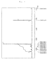
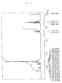
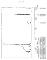
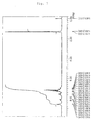
- the NMR spectrum (solvent: CDCl 3 ) was obtained by means of a Fourier-transform NMR spectrometer (R-1900 (90 MHz), product of Hitachi, Ltd.).
- An indium tin oxide transparent electrode (thickness: 120 nm) was formed on a glass substrate (25 ⁇ 75 ⁇ 1.1 mm).
- the glass substrate was cleaned through irradiation with a UV ray in an ozone atmosphere, and placed in a vacuum deposition apparatus.
- Example 1 The procedure of Example 1 was repeated, except that compound (5) was used instead of compound (2), to thereby fabricate an organic EL device.
- Example 1 The procedure of Example 1 was repeated, except that compound (11) was used instead of compound (2), to thereby fabricate an organic EL device.
- Example 1 The procedure of Example 1 was repeated, except that 6,12-bis(diphenylamino)chrysene was used instead of compound (2), to thereby fabricate an organic EL device.
- the organic EL device including the organic EL device material of the present invention serving as a light-emitting material attains emission luminance sufficient for use in practice through low applied voltage.
- the device also attains high emission efficiency and has a long service life; i.e., does not severely deteriorated during use for a long period of time.
Landscapes
- Chemical & Material Sciences (AREA)
- Engineering & Computer Science (AREA)
- Materials Engineering (AREA)
- Physics & Mathematics (AREA)
- Spectroscopy & Molecular Physics (AREA)
- Organic Chemistry (AREA)
- Electroluminescent Light Sources (AREA)
- Organic Low-Molecular-Weight Compounds And Preparation Thereof (AREA)
- Treatments For Attaching Organic Compounds To Fibrous Goods (AREA)
- Chemical Or Physical Treatment Of Fibers (AREA)
- Illuminated Signs And Luminous Advertising (AREA)
Abstract
Description
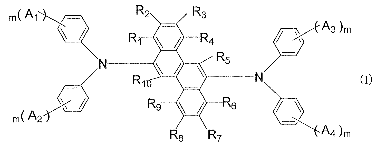

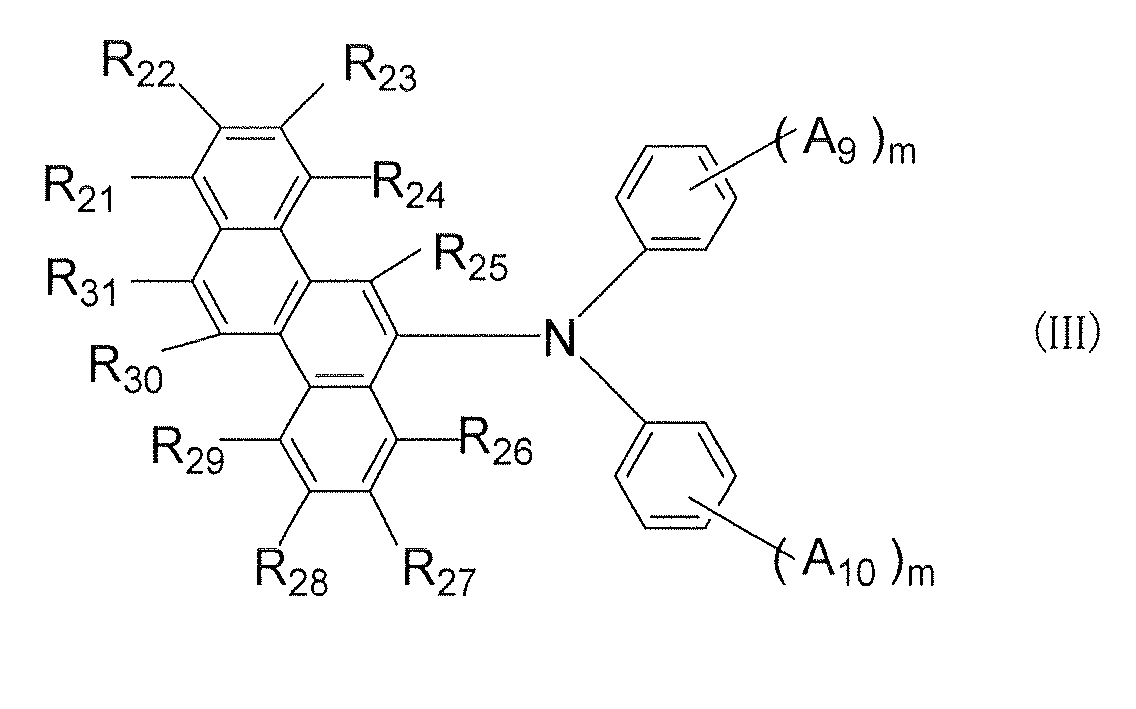

with the proviso that in formula (I), at least one of A1 to A4 does not represent a hydrogen atom, that in formula (II), at least one of A5 to A8 does not represent a hydrogen atom, that in formula (III), at least one of A9 and A10 does not represent a hydrogen atom, and that in formula (IV), at least one of A11 and A12 does not represent a hydrogen atom;
each of R1 to R42 represents a hydrogen atom, a substituted or unsubstituted alkyl group having 1 to 20 carbon atoms, a substituted or unsubstituted aryl group having 6 to 20 ring carbon atoms, or a cyano group; and
each of X1 to X3 represents a substituted or unsubstituted arylene group having 6 to 20 ring carbon atoms).


Claims (7)
- An organic electroluminescent device material comprising an aromatic amine derivative represented by any of the following formulas (I) to (IV):

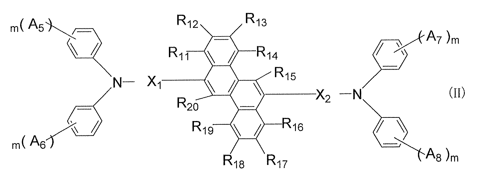
 (wherein each of A1 to A12 represents a hydrogen atom, a substituted or unsubstituted alkyl group having 1 to 50 carbon atoms, a substituted or unsubstituted aryl group having 5 to 50 ring carbon atoms, a substituted or unsubstituted cycloalkyl group having 3 to 50 ring carbon atoms, a substituted or unsubstituted alkoxyl group having 1 to 50 carbon atoms, a substituted or unsubstituted aryloxy group having 5 to 50 ring carbon atoms, a substituted or unsubstituted arylamino group having 5 to 50 ring carbon atoms, a substituted or unsubstituted alkylamino group having 1 to 20 carbon atoms, or a halogen atom; m is an integer of 0 to 5, and when m is 2 or more, groups represented by any of A1 to A12 may be identical to or different from one another, or may be linked together to form a saturated or unsaturated ring; each pair of A1 and A2, A3 and A4, A5 and A6, A7 and A8, A9 and A10, and A11 and A12 is such that the members thereof may be linked together to form a saturated or unsaturated ring;
with the proviso that in formula (I), at least one of A1 to A4 does not represent a hydrogen atom, that in formula (II), at least one of A5 to A8 does not represent a hydrogen atom; that in formula (III), at least one of A9 and A10 does not represent a hydrogen atom, and that in formula (IV), at least one of A11 and A12 does not represent a hydrogen atom;
each of R1 to R42 represents a hydrogen atom, a substituted or unsubstituted alkyl group having 1 to 20 carbon atoms, a substituted or unsubstituted aryl group having 6 to 20 ring carbon atoms, or a cyano group; and
each of X1 to X3 represents a substituted or unsubstituted arylene group having 6 to 20 ring carbon atoms). - An organic electroluminescent device material as described in claim 1, which is a light-emitting material for use in an organic electroluminescent device.
- An organic electroluminescent device comprising a cathode, an anode, and one or more organic thin-film layers interposed between the cathode and the anode, the organic thin-layers including at least a light-emitting layer, wherein at least one of the organic thin-film layers contains the organic electroluminescent device material as recited in claim 1 in the form of single component material or a mixture of a plurality of components.
- An organic electroluminescent device comprising a cathode, an anode, and one or more organic thin-film layers interposed between the cathode and the anode, the organic thin-layers including at least a light-emitting layer, wherein the light-emitting layer contains the organic electroluminescent device material as recited in claim 1 in an amount of 0.1 to 20 wt.%.
- An organic electroluminescent device as described in claim 3, which further includes a layer containing an aromatic tertiary amine derivative and/or a phthalocyanine derivative, the layer being provided between the light-emitting layer and the anode.
- An organic electroluminescent device as described in claim 4, which further includes a layer containing an aromatic tertiary amine derivative and/or a phthalocyanine derivative, the layer being provided between the light-emitting layer and the anode.
- An organic electroluminescent device as described in any of claims 3 to 6, which emits blue light.
Applications Claiming Priority (3)
| Application Number | Priority Date | Filing Date | Title |
|---|---|---|---|
| JP2002327956 | 2002-11-12 | ||
| JP2002327956 | 2002-11-12 | ||
| PCT/JP2003/013366 WO2004044088A1 (en) | 2002-11-12 | 2003-10-20 | Material for organic electroluminescent device and organic electroluminescent device using same |
Publications (3)
| Publication Number | Publication Date |
|---|---|
| EP1561794A1 true EP1561794A1 (en) | 2005-08-10 |
| EP1561794A4 EP1561794A4 (en) | 2008-08-20 |
| EP1561794B1 EP1561794B1 (en) | 2010-06-30 |
Family
ID=32310532
Family Applications (1)
| Application Number | Title | Priority Date | Filing Date |
|---|---|---|---|
| EP03754188A Expired - Lifetime EP1561794B1 (en) | 2002-11-12 | 2003-10-20 | Material for organic electroluminescent device and organic electroluminescent device using same |
Country Status (9)
| Country | Link |
|---|---|
| US (3) | US20060052641A1 (en) |
| EP (1) | EP1561794B1 (en) |
| JP (1) | JP4205059B2 (en) |
| KR (1) | KR101031719B1 (en) |
| CN (2) | CN1978586A (en) |
| AT (1) | ATE472585T1 (en) |
| DE (1) | DE60333214D1 (en) |
| TW (1) | TW200420709A (en) |
| WO (1) | WO2004044088A1 (en) |
Cited By (26)
| Publication number | Priority date | Publication date | Assignee | Title |
|---|---|---|---|---|
| EP1533290A4 (en) * | 2002-08-12 | 2007-07-04 | Idemitsu Kosan Co | OLIGOARYLENE DERIVATIVES AND ORGANIC ELECTROLUMINESCENT DEVICES MADE BY USING THESE DERIVATIVES |
| EP1792893A4 (en) * | 2004-08-31 | 2007-11-21 | Idemitsu Kosan Co | AROMATIC AMINE DERIVATIVE AND ORGANIC ELECTROLUMINESCENT DEVICE USING THE SAME |
| WO2008147721A1 (en) * | 2007-06-01 | 2008-12-04 | E. I. Du Pont De Nemours And Company | Chrysenes for blue luminescent applications |
| WO2008150872A1 (en) * | 2007-06-01 | 2008-12-11 | E.I. Du Pont De Nemours And Company | Chrysenes for deep blue luminescent applications |
| WO2008150940A1 (en) * | 2007-06-01 | 2008-12-11 | E. I. Du Pont De Nemours And Company | Chrysenes for green luminescent applications |
| US7642380B2 (en) | 2006-03-03 | 2010-01-05 | Idemitsu Kosan Co., Ltd. | Aromatic amine derivative and organic electroluminescence device using the same |
| US7737628B2 (en) | 2005-02-07 | 2010-06-15 | Idemitsu Kosan Co., Ltd. | Aromatic amine derivative and organic electroluminescence device using the same |
| US7816017B2 (en) | 2005-03-15 | 2010-10-19 | Idemitsu Kosan Co., Ltd. | Aromatic amine derivative and organic electroluminescence device using the same |
| US8115378B2 (en) | 2006-12-28 | 2012-02-14 | E. I. Du Pont De Nemours And Company | Tetra-substituted chrysenes for luminescent applications |
| US8263973B2 (en) | 2008-12-19 | 2012-09-11 | E I Du Pont De Nemours And Company | Anthracene compounds for luminescent applications |
| US8273468B2 (en) | 2007-06-01 | 2012-09-25 | E I Du Pont De Nemours And Company | Green luminescent materials |
| US8431245B2 (en) | 2009-09-29 | 2013-04-30 | E. I. Du Pont De Nemours And Company | Deuterated compounds for luminescent applications |
| US8471247B2 (en) | 2009-08-24 | 2013-06-25 | E I Du Pont De Nemours And Company | Organic light-emitting diode luminaires |
| US8476620B2 (en) | 2009-08-24 | 2013-07-02 | E I Du Pont De Nemours And Company | Organic light-emitting diode luminaires |
| US8497495B2 (en) | 2009-04-03 | 2013-07-30 | E I Du Pont De Nemours And Company | Electroactive materials |
| US8531100B2 (en) | 2008-12-22 | 2013-09-10 | E I Du Pont De Nemours And Company | Deuterated compounds for luminescent applications |
| US8546844B2 (en) | 2008-06-26 | 2013-10-01 | E I Du Pont De Nemours And Company | Process for forming an organic light-emitting diode luminaires having a single light-emitting layer with at least two light-emitting dopants |
| US8617720B2 (en) | 2009-12-21 | 2013-12-31 | E I Du Pont De Nemours And Company | Electroactive composition and electronic device made with the composition |
| US8674343B2 (en) | 2009-10-29 | 2014-03-18 | E I Du Pont De Nemours And Company | Organic light-emitting diodes having white light emission |
| US8759818B2 (en) | 2009-02-27 | 2014-06-24 | E I Du Pont De Nemours And Company | Deuterated compounds for electronic applications |
| US8932733B2 (en) | 2008-12-19 | 2015-01-13 | E I Du Pont De Nemours And Company | Chrysene derivative host materials |
| US8968883B2 (en) | 2009-08-13 | 2015-03-03 | E I Du Pont De Nemours And Company | Chrysene derivative materials |
| US9133095B2 (en) | 2009-07-01 | 2015-09-15 | E I Du Pont De Nemours And Company | Chrysene compounds for luminescent applications |
| US9260657B2 (en) | 2009-05-19 | 2016-02-16 | E I Du Pont De Nemours And Company | Chrysene compounds for luminescent applications |
| US9293716B2 (en) | 2010-12-20 | 2016-03-22 | Ei Du Pont De Nemours And Company | Compositions for electronic applications |
| US9496506B2 (en) | 2009-10-29 | 2016-11-15 | E I Du Pont De Nemours And Company | Deuterated compounds for electronic applications |
Families Citing this family (57)
| Publication number | Priority date | Publication date | Assignee | Title |
|---|---|---|---|---|
| KR100743337B1 (en) * | 1998-12-28 | 2007-07-26 | 이데미쓰 고산 가부시키가이샤 | Organic electroluminescent element |
| US7829444B2 (en) * | 2004-11-10 | 2010-11-09 | Canon Kabushiki Kaisha | Field effect transistor manufacturing method |
| JP5091854B2 (en) | 2006-04-18 | 2012-12-05 | 出光興産株式会社 | Aromatic amine derivative and organic electroluminescence device using the same |
| JP4702191B2 (en) * | 2006-06-16 | 2011-06-15 | 日本ビクター株式会社 | Reflective liquid crystal display |
| US8257836B2 (en) | 2006-12-29 | 2012-09-04 | E I Du Pont De Nemours And Company | Di-substituted pyrenes for luminescent applications |
| US8227094B2 (en) * | 2007-04-27 | 2012-07-24 | Canon Kabushiki Kaisha | Organic electroluminescent device |
| JP5292394B2 (en) * | 2007-06-01 | 2013-09-18 | イー・アイ・デュポン・ドウ・ヌムール・アンド・カンパニー | Blue light emitting material |
| WO2008149968A1 (en) * | 2007-06-07 | 2008-12-11 | Idemitsu Kosan Co., Ltd. | Aromatic amine derivative and organic electroluminescent device |
| KR20100017832A (en) * | 2007-06-18 | 2010-02-16 | 이데미쓰 고산 가부시키가이샤 | Trinaphthyl monoamine or derivative thereof, organic electroluminescent device using the same, and organic electroluminescent material-containing solution |
| JP2010245060A (en) * | 2007-07-07 | 2010-10-28 | Idemitsu Kosan Co Ltd | Organic EL device |
| EP2213693A4 (en) | 2007-11-20 | 2011-11-09 | Idemitsu Kosan Co | POLYMERIC COMPOUND AND ORGANIC ELECTROLUMINESCENT ELEMENT COMPRISING SAME |
| US20100259163A1 (en) | 2007-12-11 | 2010-10-14 | Idemitsu Kosan Co., Ltd. | Polymer compound and organic electroluminescent device using the same |
| WO2009075203A1 (en) | 2007-12-11 | 2009-06-18 | Idemitsu Kosan Co., Ltd. | Polymer compound and organic electroluminescent device using the same |
| KR20100097182A (en) * | 2007-12-28 | 2010-09-02 | 이데미쓰 고산 가부시키가이샤 | Aromatic diamine derivative and organic electroluminescent device using the same |
| US8192848B2 (en) | 2008-01-11 | 2012-06-05 | E I Du Pont De Nemours And Company | Substituted pyrenes and associated production methods for luminescent applications |
| KR101807644B1 (en) | 2008-02-27 | 2017-12-11 | 도레이 카부시키가이샤 | Luminescent element material and luminescent element |
| JP5491383B2 (en) | 2008-03-19 | 2014-05-14 | 出光興産株式会社 | Anthracene derivatives, light emitting materials, and organic electroluminescence devices |
| KR20110063747A (en) | 2008-08-29 | 2011-06-14 | 이데미쓰 고산 가부시키가이샤 | Compound for organic thin film transistor and organic thin film transistor using same |
| JP5687628B2 (en) * | 2008-11-19 | 2015-03-18 | イー・アイ・デュポン・ドウ・ヌムール・アンド・カンパニーE.I.Du Pont De Nemours And Company | Chrysene compounds for blue or green luminescence applications |
| KR101528658B1 (en) * | 2008-12-12 | 2015-06-12 | 이 아이 듀폰 디 네모아 앤드 캄파니 | Photoactive composition and electronic device made with the composition |
| US20100186806A1 (en) * | 2009-01-26 | 2010-07-29 | Mitsubishi Electric Corporation | Photovoltaic module |
| JP2012519186A (en) * | 2009-02-27 | 2012-08-23 | イー・アイ・デュポン・ドウ・ヌムール・アンド・カンパニー | Deuterium compounds for electronic applications |
| JP5676579B2 (en) * | 2009-05-19 | 2015-02-25 | イー・アイ・デュポン・ドウ・ヌムール・アンド・カンパニーE.I.Du Pont De Nemours And Company | Deuterium compounds for electronic applications |
| US20100295444A1 (en) | 2009-05-22 | 2010-11-25 | Idemitsu Kosan Co., Ltd. | Organic electroluminescence device |
| US20100295445A1 (en) | 2009-05-22 | 2010-11-25 | Idemitsu Kosan Co., Ltd. | Organic electroluminescent device |
| US20100314644A1 (en) | 2009-06-12 | 2010-12-16 | Idemitsu Kosan Co., Ltd. | Organic electroluminescent device |
| WO2011014216A1 (en) * | 2009-07-27 | 2011-02-03 | E. I. Du Pont De Nemours And Company | Process and materials for making contained layers and devices made with same |
| JP2013508380A (en) | 2009-10-19 | 2013-03-07 | イー・アイ・デュポン・ドウ・ヌムール・アンド・カンパニー | Triarylamine compounds for electronic applications |
| WO2011049904A2 (en) | 2009-10-19 | 2011-04-28 | E. I. Du Pont De Nemours And Company | Triarylamine compounds for electronic applications |
| TW201119976A (en) * | 2009-12-09 | 2011-06-16 | Du Pont | Deuterated compound as part of a combination of compounds for electronic applications |
| KR101736987B1 (en) | 2010-04-06 | 2017-05-18 | 삼성디스플레이 주식회사 | Heterocyclic compound and organic light emitting device comprising the same |
| KR101758328B1 (en) | 2010-04-06 | 2017-07-17 | 삼성디스플레이 주식회사 | Heterocyclic compound and organic light emitting device comprising the same |
| JP4579343B1 (en) * | 2010-04-23 | 2010-11-10 | 富士フイルム株式会社 | Organic electroluminescent element material and organic electroluminescent element |
| KR101810045B1 (en) | 2010-10-25 | 2017-12-19 | 삼성디스플레이 주식회사 | Heterocyclic compound and Organic light emitting device containing same |
| US8455867B2 (en) | 2010-10-26 | 2013-06-04 | Samsung Display Co., Ltd. | Organic light-emitting device |
| CN102668160B (en) | 2010-11-22 | 2016-06-22 | 出光兴产株式会社 | Organic electroluminescent device |
| TWI518078B (en) * | 2010-12-28 | 2016-01-21 | 半導體能源研究所股份有限公司 | Benzo[b]naphtho[1,2-d]furan compound serving as a light-emitting element material |
| KR101894024B1 (en) | 2011-04-22 | 2018-09-03 | 삼성디스플레이 주식회사 | Heterocyclic compound and Organic light emitting device comprising the same |
| KR101873447B1 (en) * | 2011-06-22 | 2018-07-03 | 삼성디스플레이 주식회사 | Novel compound and organic light emitting device containing same |
| CN103380508B (en) | 2011-11-22 | 2017-09-08 | 出光兴产株式会社 | Aromatic heterocyclic derivative, material for organic electroluminescent element, and organic electroluminescent element |
| JP2015051925A (en) * | 2011-11-25 | 2015-03-19 | 出光興産株式会社 | Aromatic amine derivative and organic electroluminescent element using the same |
| CN103840089B (en) | 2012-11-20 | 2016-12-21 | 群康科技(深圳)有限公司 | Oled device and display floater thereof |
| KR102050484B1 (en) | 2013-03-04 | 2019-12-02 | 삼성디스플레이 주식회사 | Anthracene derivatives and organic light emitting diodes comprising the derivatives |
| KR102107106B1 (en) | 2013-05-09 | 2020-05-07 | 삼성디스플레이 주식회사 | Styryl-based compound and organic light emitting diode comprising the same |
| KR102269131B1 (en) | 2013-07-01 | 2021-06-25 | 삼성디스플레이 주식회사 | Compound and organic light emitting device comprising same |
| US10062850B2 (en) | 2013-12-12 | 2018-08-28 | Samsung Display Co., Ltd. | Amine-based compounds and organic light-emitting devices comprising the same |
| KR20150132795A (en) | 2014-05-16 | 2015-11-26 | 삼성디스플레이 주식회사 | Organic light emitting device |
| KR102327086B1 (en) | 2014-06-11 | 2021-11-17 | 삼성디스플레이 주식회사 | Organic light-emitting devices |
| KR102322013B1 (en) | 2014-12-12 | 2021-11-05 | 삼성디스플레이 주식회사 | Condensed-cyclic compound and organic light emitting device comprising the same |
| KR102343145B1 (en) | 2015-01-12 | 2021-12-27 | 삼성디스플레이 주식회사 | Condensed compound and organic light-emitting device comprising the same |
| US9887372B2 (en) | 2015-06-11 | 2018-02-06 | Samsung Display Co., Ltd. | Amine-based compound and organic light-emitting device including the same |
| US9954187B2 (en) | 2016-04-08 | 2018-04-24 | Idemitsu Kosan Co., Ltd. | Compound, organic electroluminescence device and electronic device |
| JP2021177443A (en) | 2018-05-28 | 2021-11-11 | 出光興産株式会社 | Organic electroluminescent element, display device and electronic apparatus |
| US12583814B2 (en) | 2021-02-16 | 2026-03-24 | Lg Chem, Ltd. | Compound and organic light emitting device comprising the same |
| CN116438154B (en) * | 2021-02-16 | 2026-01-02 | 株式会社Lg化学 | New compounds and organic light-emitting devices containing them |
| TWI816307B (en) * | 2021-02-19 | 2023-09-21 | 南韓商Lg化學股份有限公司 | Organic light emitting device |
| EP4369902A4 (en) | 2021-07-07 | 2024-12-04 | LG Chem, Ltd. | COMPOUND AND ORGANIC LIGHT-EMITTING DEVICE THEREOF |
Family Cites Families (21)
| Publication number | Priority date | Publication date | Assignee | Title |
|---|---|---|---|---|
| US5219692A (en) * | 1989-03-29 | 1993-06-15 | Ricoh Company, Ltd. | Electrophotographic photoconductors and tertiary amine compounds having condensed polycyclic group for use in the same |
| JP3035622B2 (en) * | 1989-03-29 | 2000-04-24 | 株式会社リコー | Tertiary amine compounds having fused polycyclic groups |
| US5153072A (en) * | 1989-08-31 | 1992-10-06 | The Board Of Regents Of The University Of Washington | Method of controlling the chemical structure of polymeric films by plasma deposition and films produced thereby |
| US5081569A (en) * | 1989-09-05 | 1992-01-14 | Spaulding Lighting, Inc. | Luminaire with changeable accent lighting |
| JPH04175395A (en) * | 1990-07-06 | 1992-06-23 | Ricoh Co Ltd | Electroluminescent |
| US5061569A (en) * | 1990-07-26 | 1991-10-29 | Eastman Kodak Company | Electroluminescent device with organic electroluminescent medium |
| US5536949A (en) * | 1992-08-28 | 1996-07-16 | Idemistu Kosan Co., Ltd. | Charge injection auxiliary material and organic electroluminescence device containing the same |
| JPH06240245A (en) * | 1993-02-17 | 1994-08-30 | Ricoh Co Ltd | Electroluminescent device |
| JP3712760B2 (en) * | 1995-05-17 | 2005-11-02 | Tdk株式会社 | Organic EL device |
| JP3503403B2 (en) * | 1997-03-17 | 2004-03-08 | 東洋インキ製造株式会社 | Light emitting material for organic electroluminescent device and organic electroluminescent device using the same |
| DE19738697C1 (en) | 1997-08-29 | 1998-11-26 | Siemens Ag | High voltage load switch with driven counter contact piece |
| JP4117093B2 (en) * | 1998-12-28 | 2008-07-09 | 出光興産株式会社 | Material for organic electroluminescence device and organic electroluminescence device using the same |
| KR100743337B1 (en) * | 1998-12-28 | 2007-07-26 | 이데미쓰 고산 가부시키가이샤 | Organic electroluminescent element |
| JP4220669B2 (en) * | 2000-12-26 | 2009-02-04 | 出光興産株式会社 | Organic electroluminescence device |
| KR100577179B1 (en) * | 2001-10-30 | 2006-05-10 | 엘지전자 주식회사 | Organic electroluminescent element |
| EP1541657B2 (en) * | 2002-07-19 | 2014-03-05 | Idemitsu Kosan Co., Ltd. | Organic electroluminescent devices and organic luminescent medium |
| EP1792893A4 (en) * | 2004-08-31 | 2007-11-21 | Idemitsu Kosan Co | AROMATIC AMINE DERIVATIVE AND ORGANIC ELECTROLUMINESCENT DEVICE USING THE SAME |
| KR101267124B1 (en) * | 2005-02-07 | 2013-05-23 | 이데미쓰 고산 가부시키가이샤 | Aromatic amine derivative and organic electroluminescent device using same |
| JP4263700B2 (en) * | 2005-03-15 | 2009-05-13 | 出光興産株式会社 | Aromatic amine derivative and organic electroluminescence device using the same |
| JP2007137837A (en) * | 2005-11-21 | 2007-06-07 | Idemitsu Kosan Co Ltd | Aromatic amine derivative and organic electroluminescence device using the same |
| JP2007230960A (en) * | 2006-03-03 | 2007-09-13 | Idemitsu Kosan Co Ltd | Aromatic amine derivative and organic electroluminescence device using the same |
-
2003
- 2003-10-20 CN CNA2006101436831A patent/CN1978586A/en active Pending
- 2003-10-20 JP JP2004551191A patent/JP4205059B2/en not_active Expired - Fee Related
- 2003-10-20 CN CNB2003801031007A patent/CN100343359C/en not_active Expired - Fee Related
- 2003-10-20 US US10/532,794 patent/US20060052641A1/en not_active Abandoned
- 2003-10-20 WO PCT/JP2003/013366 patent/WO2004044088A1/en not_active Ceased
- 2003-10-20 KR KR1020057008392A patent/KR101031719B1/en not_active Expired - Fee Related
- 2003-10-20 AT AT03754188T patent/ATE472585T1/en not_active IP Right Cessation
- 2003-10-20 DE DE60333214T patent/DE60333214D1/en not_active Expired - Lifetime
- 2003-10-20 EP EP03754188A patent/EP1561794B1/en not_active Expired - Lifetime
- 2003-10-23 TW TW092129473A patent/TW200420709A/en not_active IP Right Cessation
-
2007
- 2007-02-28 US US11/711,655 patent/US20070155991A1/en not_active Abandoned
-
2009
- 2009-01-09 US US12/318,859 patent/US8178218B2/en not_active Expired - Fee Related
Cited By (33)
| Publication number | Priority date | Publication date | Assignee | Title |
|---|---|---|---|---|
| EP1533290A4 (en) * | 2002-08-12 | 2007-07-04 | Idemitsu Kosan Co | OLIGOARYLENE DERIVATIVES AND ORGANIC ELECTROLUMINESCENT DEVICES MADE BY USING THESE DERIVATIVES |
| EP1792893A4 (en) * | 2004-08-31 | 2007-11-21 | Idemitsu Kosan Co | AROMATIC AMINE DERIVATIVE AND ORGANIC ELECTROLUMINESCENT DEVICE USING THE SAME |
| US7425653B2 (en) | 2004-08-31 | 2008-09-16 | Idemitsu Kosan Co., Ltd. | Aromatic amine derivative and organic electroluminescence device employing the same |
| US7524568B2 (en) | 2004-08-31 | 2009-04-28 | Idemitsu Kosan Co., Ltd. | Aromatic amine derivative and organic electroluminescence device employing the same |
| US7737628B2 (en) | 2005-02-07 | 2010-06-15 | Idemitsu Kosan Co., Ltd. | Aromatic amine derivative and organic electroluminescence device using the same |
| US7816017B2 (en) | 2005-03-15 | 2010-10-19 | Idemitsu Kosan Co., Ltd. | Aromatic amine derivative and organic electroluminescence device using the same |
| US8058478B2 (en) | 2005-03-15 | 2011-11-15 | Idemitsu Kosan Co., Ltd. | Aromatic amine derivative and organic electroluminescence device using the same |
| US7642380B2 (en) | 2006-03-03 | 2010-01-05 | Idemitsu Kosan Co., Ltd. | Aromatic amine derivative and organic electroluminescence device using the same |
| US8115378B2 (en) | 2006-12-28 | 2012-02-14 | E. I. Du Pont De Nemours And Company | Tetra-substituted chrysenes for luminescent applications |
| WO2008150872A1 (en) * | 2007-06-01 | 2008-12-11 | E.I. Du Pont De Nemours And Company | Chrysenes for deep blue luminescent applications |
| WO2008150940A1 (en) * | 2007-06-01 | 2008-12-11 | E. I. Du Pont De Nemours And Company | Chrysenes for green luminescent applications |
| US8158831B2 (en) | 2007-06-01 | 2012-04-17 | E I Du Pont De Nemours And Company | Chrysene compounds for deep blue luminescent applications |
| US8273468B2 (en) | 2007-06-01 | 2012-09-25 | E I Du Pont De Nemours And Company | Green luminescent materials |
| WO2008147721A1 (en) * | 2007-06-01 | 2008-12-04 | E. I. Du Pont De Nemours And Company | Chrysenes for blue luminescent applications |
| US8604247B2 (en) | 2007-06-01 | 2013-12-10 | E I Du Pont De Nemours And Company | Chrysenes for deep blue luminescent applications |
| US8546844B2 (en) | 2008-06-26 | 2013-10-01 | E I Du Pont De Nemours And Company | Process for forming an organic light-emitting diode luminaires having a single light-emitting layer with at least two light-emitting dopants |
| US8263973B2 (en) | 2008-12-19 | 2012-09-11 | E I Du Pont De Nemours And Company | Anthracene compounds for luminescent applications |
| US8932733B2 (en) | 2008-12-19 | 2015-01-13 | E I Du Pont De Nemours And Company | Chrysene derivative host materials |
| US8531100B2 (en) | 2008-12-22 | 2013-09-10 | E I Du Pont De Nemours And Company | Deuterated compounds for luminescent applications |
| US8759818B2 (en) | 2009-02-27 | 2014-06-24 | E I Du Pont De Nemours And Company | Deuterated compounds for electronic applications |
| US8890131B2 (en) | 2009-02-27 | 2014-11-18 | E I Du Pont De Nemours And Company | Deuterated compounds for electronic applications |
| US8497495B2 (en) | 2009-04-03 | 2013-07-30 | E I Du Pont De Nemours And Company | Electroactive materials |
| US9260657B2 (en) | 2009-05-19 | 2016-02-16 | E I Du Pont De Nemours And Company | Chrysene compounds for luminescent applications |
| US9133095B2 (en) | 2009-07-01 | 2015-09-15 | E I Du Pont De Nemours And Company | Chrysene compounds for luminescent applications |
| US8968883B2 (en) | 2009-08-13 | 2015-03-03 | E I Du Pont De Nemours And Company | Chrysene derivative materials |
| US8471247B2 (en) | 2009-08-24 | 2013-06-25 | E I Du Pont De Nemours And Company | Organic light-emitting diode luminaires |
| US8772767B2 (en) | 2009-08-24 | 2014-07-08 | E I Du Pont De Nemours And Company | Organic light-emitting diode luminaires |
| US8476620B2 (en) | 2009-08-24 | 2013-07-02 | E I Du Pont De Nemours And Company | Organic light-emitting diode luminaires |
| US8431245B2 (en) | 2009-09-29 | 2013-04-30 | E. I. Du Pont De Nemours And Company | Deuterated compounds for luminescent applications |
| US8674343B2 (en) | 2009-10-29 | 2014-03-18 | E I Du Pont De Nemours And Company | Organic light-emitting diodes having white light emission |
| US9496506B2 (en) | 2009-10-29 | 2016-11-15 | E I Du Pont De Nemours And Company | Deuterated compounds for electronic applications |
| US8617720B2 (en) | 2009-12-21 | 2013-12-31 | E I Du Pont De Nemours And Company | Electroactive composition and electronic device made with the composition |
| US9293716B2 (en) | 2010-12-20 | 2016-03-22 | Ei Du Pont De Nemours And Company | Compositions for electronic applications |
Also Published As
| Publication number | Publication date |
|---|---|
| ATE472585T1 (en) | 2010-07-15 |
| EP1561794B1 (en) | 2010-06-30 |
| EP1561794A4 (en) | 2008-08-20 |
| WO2004044088A1 (en) | 2004-05-27 |
| CN100343359C (en) | 2007-10-17 |
| TW200420709A (en) | 2004-10-16 |
| US20070155991A1 (en) | 2007-07-05 |
| JP4205059B2 (en) | 2009-01-07 |
| US8178218B2 (en) | 2012-05-15 |
| US20060052641A1 (en) | 2006-03-09 |
| CN1978586A (en) | 2007-06-13 |
| TWI327159B (en) | 2010-07-11 |
| JPWO2004044088A1 (en) | 2006-03-09 |
| KR101031719B1 (en) | 2011-04-29 |
| DE60333214D1 (en) | 2010-08-12 |
| US20090195149A1 (en) | 2009-08-06 |
| KR20050086518A (en) | 2005-08-30 |
| CN1711334A (en) | 2005-12-21 |
Similar Documents
| Publication | Publication Date | Title |
|---|---|---|
| EP1561794B1 (en) | Material for organic electroluminescent device and organic electroluminescent device using same | |
| EP0866110B1 (en) | Light-emitting material for organo-electroluminescence device and organic electroluminescence device | |
| JP4188369B2 (en) | Aromatic amine derivatives | |
| EP0786926B1 (en) | Light-emitting material for organo-electroluminescence device and organo-electroluminescence devive for which the light-emitting material is adapted | |
| EP0765106B1 (en) | Light-emitting material for organic electroluminescence device, and organic electroluminescence device for which the light-emitting material is adapted | |
| JP4267623B2 (en) | Aromatic amine derivative and organic electroluminescence device using the same | |
| JP4464070B2 (en) | Arylamine compound and organic electroluminescence device using the same | |
| KR100868144B1 (en) | Novel styryl compounds and organic electroluminescent devices | |
| JP3498533B2 (en) | Light emitting material for organic electroluminescent device and organic electroluminescent device using the same | |
| JP3666086B2 (en) | Luminescent material for organic electroluminescence device and organic electroluminescence device using the same | |
| JPH09268283A (en) | Light emitting material for organic electroluminescence device and organic electroluminescence device using the same | |
| EP1138744A1 (en) | Organic electroluminescent element | |
| JPWO2002020459A1 (en) | Novel styryl compounds and organic electroluminescent devices | |
| JP3924943B2 (en) | Organic electroluminescent device material and organic electroluminescent device using the same | |
| JP3994573B2 (en) | Material for organic electroluminescence device and organic electroluminescence device using the same | |
| JP2924809B2 (en) | Light-emitting materials for organic electroluminescence devices | |
| JPH1072581A (en) | Light emitting material for organic electroluminescent device and organic electroluminescent device using the same | |
| JP2000053956A (en) | Light emitting material for organic electroluminescent device and organic electroluminescent device using the same | |
| JP3985895B2 (en) | Material for organic electroluminescence device and organic electroluminescence device using the same | |
| JPH09165573A (en) | Light emitting material for organic electroluminescence device and organic electroluminescence device using the same | |
| JP2007284684A (en) | Material for organic electroluminescence device and organic electroluminescence device using the same |
Legal Events
| Date | Code | Title | Description |
|---|---|---|---|
| PUAI | Public reference made under article 153(3) epc to a published international application that has entered the european phase |
Free format text: ORIGINAL CODE: 0009012 |
|
| 17P | Request for examination filed |
Effective date: 20050419 |
|
| AK | Designated contracting states |
Kind code of ref document: A1 Designated state(s): AT BE BG CH CY CZ DE DK EE ES FI FR GB GR HU IE IT LI LU MC NL PT RO SE SI SK TR |
|
| A4 | Supplementary search report drawn up and despatched |
Effective date: 20080723 |
|
| 17Q | First examination report despatched |
Effective date: 20081002 |
|
| GRAC | Information related to communication of intention to grant a patent modified |
Free format text: ORIGINAL CODE: EPIDOSCIGR1 |
|
| GRAP | Despatch of communication of intention to grant a patent |
Free format text: ORIGINAL CODE: EPIDOSNIGR1 |
|
| GRAS | Grant fee paid |
Free format text: ORIGINAL CODE: EPIDOSNIGR3 |
|
| GRAA | (expected) grant |
Free format text: ORIGINAL CODE: 0009210 |
|
| AK | Designated contracting states |
Kind code of ref document: B1 Designated state(s): AT BE BG CH CY CZ DE DK EE ES FI FR GB GR HU IE IT LI LU MC NL PT RO SE SI SK TR |
|
| REG | Reference to a national code |
Ref country code: CH Ref legal event code: EP Ref country code: GB Ref legal event code: FG4D |
|
| REG | Reference to a national code |
Ref country code: IE Ref legal event code: FG4D |
|
| REF | Corresponds to: |
Ref document number: 60333214 Country of ref document: DE Date of ref document: 20100812 Kind code of ref document: P |
|
| REG | Reference to a national code |
Ref country code: NL Ref legal event code: VDEP Effective date: 20100630 |
|
| PG25 | Lapsed in a contracting state [announced via postgrant information from national office to epo] |
Ref country code: SE Free format text: LAPSE BECAUSE OF FAILURE TO SUBMIT A TRANSLATION OF THE DESCRIPTION OR TO PAY THE FEE WITHIN THE PRESCRIBED TIME-LIMIT Effective date: 20100630 |
|
| PG25 | Lapsed in a contracting state [announced via postgrant information from national office to epo] |
Ref country code: SI Free format text: LAPSE BECAUSE OF FAILURE TO SUBMIT A TRANSLATION OF THE DESCRIPTION OR TO PAY THE FEE WITHIN THE PRESCRIBED TIME-LIMIT Effective date: 20100630 Ref country code: FI Free format text: LAPSE BECAUSE OF FAILURE TO SUBMIT A TRANSLATION OF THE DESCRIPTION OR TO PAY THE FEE WITHIN THE PRESCRIBED TIME-LIMIT Effective date: 20100630 Ref country code: AT Free format text: LAPSE BECAUSE OF FAILURE TO SUBMIT A TRANSLATION OF THE DESCRIPTION OR TO PAY THE FEE WITHIN THE PRESCRIBED TIME-LIMIT Effective date: 20100630 |
|
| PG25 | Lapsed in a contracting state [announced via postgrant information from national office to epo] |
Ref country code: GR Free format text: LAPSE BECAUSE OF FAILURE TO SUBMIT A TRANSLATION OF THE DESCRIPTION OR TO PAY THE FEE WITHIN THE PRESCRIBED TIME-LIMIT Effective date: 20101001 |
|
| PG25 | Lapsed in a contracting state [announced via postgrant information from national office to epo] |
Ref country code: EE Free format text: LAPSE BECAUSE OF FAILURE TO SUBMIT A TRANSLATION OF THE DESCRIPTION OR TO PAY THE FEE WITHIN THE PRESCRIBED TIME-LIMIT Effective date: 20100630 Ref country code: NL Free format text: LAPSE BECAUSE OF FAILURE TO SUBMIT A TRANSLATION OF THE DESCRIPTION OR TO PAY THE FEE WITHIN THE PRESCRIBED TIME-LIMIT Effective date: 20100630 |
|
| PG25 | Lapsed in a contracting state [announced via postgrant information from national office to epo] |
Ref country code: SK Free format text: LAPSE BECAUSE OF FAILURE TO SUBMIT A TRANSLATION OF THE DESCRIPTION OR TO PAY THE FEE WITHIN THE PRESCRIBED TIME-LIMIT Effective date: 20100630 Ref country code: PT Free format text: LAPSE BECAUSE OF FAILURE TO SUBMIT A TRANSLATION OF THE DESCRIPTION OR TO PAY THE FEE WITHIN THE PRESCRIBED TIME-LIMIT Effective date: 20101102 Ref country code: RO Free format text: LAPSE BECAUSE OF FAILURE TO SUBMIT A TRANSLATION OF THE DESCRIPTION OR TO PAY THE FEE WITHIN THE PRESCRIBED TIME-LIMIT Effective date: 20100630 Ref country code: CZ Free format text: LAPSE BECAUSE OF FAILURE TO SUBMIT A TRANSLATION OF THE DESCRIPTION OR TO PAY THE FEE WITHIN THE PRESCRIBED TIME-LIMIT Effective date: 20100630 Ref country code: CY Free format text: LAPSE BECAUSE OF FAILURE TO SUBMIT A TRANSLATION OF THE DESCRIPTION OR TO PAY THE FEE WITHIN THE PRESCRIBED TIME-LIMIT Effective date: 20100630 Ref country code: BE Free format text: LAPSE BECAUSE OF FAILURE TO SUBMIT A TRANSLATION OF THE DESCRIPTION OR TO PAY THE FEE WITHIN THE PRESCRIBED TIME-LIMIT Effective date: 20100630 |
|
| PG25 | Lapsed in a contracting state [announced via postgrant information from national office to epo] |
Ref country code: IT Free format text: LAPSE BECAUSE OF FAILURE TO SUBMIT A TRANSLATION OF THE DESCRIPTION OR TO PAY THE FEE WITHIN THE PRESCRIBED TIME-LIMIT Effective date: 20100630 |
|
| PG25 | Lapsed in a contracting state [announced via postgrant information from national office to epo] |
Ref country code: DK Free format text: LAPSE BECAUSE OF FAILURE TO SUBMIT A TRANSLATION OF THE DESCRIPTION OR TO PAY THE FEE WITHIN THE PRESCRIBED TIME-LIMIT Effective date: 20100630 |
|
| PLBE | No opposition filed within time limit |
Free format text: ORIGINAL CODE: 0009261 |
|
| STAA | Information on the status of an ep patent application or granted ep patent |
Free format text: STATUS: NO OPPOSITION FILED WITHIN TIME LIMIT |
|
| PG25 | Lapsed in a contracting state [announced via postgrant information from national office to epo] |
Ref country code: MC Free format text: LAPSE BECAUSE OF NON-PAYMENT OF DUE FEES Effective date: 20101031 |
|
| REG | Reference to a national code |
Ref country code: CH Ref legal event code: PL |
|
| 26N | No opposition filed |
Effective date: 20110331 |
|
| PG25 | Lapsed in a contracting state [announced via postgrant information from national office to epo] |
Ref country code: ES Free format text: LAPSE BECAUSE OF FAILURE TO SUBMIT A TRANSLATION OF THE DESCRIPTION OR TO PAY THE FEE WITHIN THE PRESCRIBED TIME-LIMIT Effective date: 20101011 |
|
| REG | Reference to a national code |
Ref country code: DE Ref legal event code: R097 Ref document number: 60333214 Country of ref document: DE Effective date: 20110330 |
|
| PG25 | Lapsed in a contracting state [announced via postgrant information from national office to epo] |
Ref country code: LI Free format text: LAPSE BECAUSE OF NON-PAYMENT OF DUE FEES Effective date: 20101031 Ref country code: CH Free format text: LAPSE BECAUSE OF NON-PAYMENT OF DUE FEES Effective date: 20101031 |
|
| PG25 | Lapsed in a contracting state [announced via postgrant information from national office to epo] |
Ref country code: IE Free format text: LAPSE BECAUSE OF NON-PAYMENT OF DUE FEES Effective date: 20101020 |
|
| PG25 | Lapsed in a contracting state [announced via postgrant information from national office to epo] |
Ref country code: BG Free format text: LAPSE BECAUSE OF FAILURE TO SUBMIT A TRANSLATION OF THE DESCRIPTION OR TO PAY THE FEE WITHIN THE PRESCRIBED TIME-LIMIT Effective date: 20100630 Ref country code: LU Free format text: LAPSE BECAUSE OF NON-PAYMENT OF DUE FEES Effective date: 20101020 Ref country code: HU Free format text: LAPSE BECAUSE OF FAILURE TO SUBMIT A TRANSLATION OF THE DESCRIPTION OR TO PAY THE FEE WITHIN THE PRESCRIBED TIME-LIMIT Effective date: 20110101 |
|
| PG25 | Lapsed in a contracting state [announced via postgrant information from national office to epo] |
Ref country code: TR Free format text: LAPSE BECAUSE OF FAILURE TO SUBMIT A TRANSLATION OF THE DESCRIPTION OR TO PAY THE FEE WITHIN THE PRESCRIBED TIME-LIMIT Effective date: 20100630 |
|
| PG25 | Lapsed in a contracting state [announced via postgrant information from national office to epo] |
Ref country code: BG Free format text: LAPSE BECAUSE OF FAILURE TO SUBMIT A TRANSLATION OF THE DESCRIPTION OR TO PAY THE FEE WITHIN THE PRESCRIBED TIME-LIMIT Effective date: 20100930 |
|
| REG | Reference to a national code |
Ref country code: FR Ref legal event code: PLFP Year of fee payment: 14 |
|
| REG | Reference to a national code |
Ref country code: FR Ref legal event code: PLFP Year of fee payment: 15 |
|
| REG | Reference to a national code |
Ref country code: FR Ref legal event code: PLFP Year of fee payment: 16 |
|
| PGFP | Annual fee paid to national office [announced via postgrant information from national office to epo] |
Ref country code: FR Payment date: 20210913 Year of fee payment: 19 |
|
| PGFP | Annual fee paid to national office [announced via postgrant information from national office to epo] |
Ref country code: GB Payment date: 20210907 Year of fee payment: 19 |
|
| PGFP | Annual fee paid to national office [announced via postgrant information from national office to epo] |
Ref country code: DE Payment date: 20210908 Year of fee payment: 19 |
|
| REG | Reference to a national code |
Ref country code: DE Ref legal event code: R119 Ref document number: 60333214 Country of ref document: DE |
|
| GBPC | Gb: european patent ceased through non-payment of renewal fee |
Effective date: 20221020 |
|
| PG25 | Lapsed in a contracting state [announced via postgrant information from national office to epo] |
Ref country code: FR Free format text: LAPSE BECAUSE OF NON-PAYMENT OF DUE FEES Effective date: 20221031 Ref country code: DE Free format text: LAPSE BECAUSE OF NON-PAYMENT OF DUE FEES Effective date: 20230503 |
|
| PG25 | Lapsed in a contracting state [announced via postgrant information from national office to epo] |
Ref country code: GB Free format text: LAPSE BECAUSE OF NON-PAYMENT OF DUE FEES Effective date: 20221020 |