EP1138744A1 - Organic electroluminescent element - Google Patents
Organic electroluminescent element Download PDFInfo
- Publication number
- EP1138744A1 EP1138744A1 EP00962881A EP00962881A EP1138744A1 EP 1138744 A1 EP1138744 A1 EP 1138744A1 EP 00962881 A EP00962881 A EP 00962881A EP 00962881 A EP00962881 A EP 00962881A EP 1138744 A1 EP1138744 A1 EP 1138744A1
- Authority
- EP
- European Patent Office
- Prior art keywords
- carbon atoms
- group
- organic
- light emitting
- general formula
- Prior art date
- Legal status (The legal status is an assumption and is not a legal conclusion. Google has not performed a legal analysis and makes no representation as to the accuracy of the status listed.)
- Withdrawn
Links
Classifications
-
- C—CHEMISTRY; METALLURGY
- C09—DYES; PAINTS; POLISHES; NATURAL RESINS; ADHESIVES; COMPOSITIONS NOT OTHERWISE PROVIDED FOR; APPLICATIONS OF MATERIALS NOT OTHERWISE PROVIDED FOR
- C09K—MATERIALS FOR MISCELLANEOUS APPLICATIONS, NOT PROVIDED FOR ELSEWHERE
- C09K11/00—Luminescent, e.g. electroluminescent, chemiluminescent materials
- C09K11/06—Luminescent, e.g. electroluminescent, chemiluminescent materials containing organic luminescent materials
-
- C—CHEMISTRY; METALLURGY
- C07—ORGANIC CHEMISTRY
- C07C—ACYCLIC OR CARBOCYCLIC COMPOUNDS
- C07C211/00—Compounds containing amino groups bound to a carbon skeleton
- C07C211/43—Compounds containing amino groups bound to a carbon skeleton having amino groups bound to carbon atoms of six-membered aromatic rings of the carbon skeleton
- C07C211/54—Compounds containing amino groups bound to a carbon skeleton having amino groups bound to carbon atoms of six-membered aromatic rings of the carbon skeleton having amino groups bound to two or three six-membered aromatic rings
- C07C211/56—Compounds containing amino groups bound to a carbon skeleton having amino groups bound to carbon atoms of six-membered aromatic rings of the carbon skeleton having amino groups bound to two or three six-membered aromatic rings the carbon skeleton being further substituted by halogen atoms or by nitro or nitroso groups
-
- C—CHEMISTRY; METALLURGY
- C07—ORGANIC CHEMISTRY
- C07C—ACYCLIC OR CARBOCYCLIC COMPOUNDS
- C07C211/00—Compounds containing amino groups bound to a carbon skeleton
- C07C211/43—Compounds containing amino groups bound to a carbon skeleton having amino groups bound to carbon atoms of six-membered aromatic rings of the carbon skeleton
- C07C211/57—Compounds containing amino groups bound to a carbon skeleton having amino groups bound to carbon atoms of six-membered aromatic rings of the carbon skeleton having amino groups bound to carbon atoms of six-membered aromatic rings being part of condensed ring systems of the carbon skeleton
- C07C211/58—Naphthylamines; N-substituted derivatives thereof
-
- C—CHEMISTRY; METALLURGY
- C07—ORGANIC CHEMISTRY
- C07D—HETEROCYCLIC COMPOUNDS
- C07D209/00—Heterocyclic compounds containing five-membered rings, condensed with other rings, with one nitrogen atom as the only ring hetero atom
- C07D209/56—Ring systems containing three or more rings
- C07D209/80—[b, c]- or [b, d]-condensed
- C07D209/82—Carbazoles; Hydrogenated carbazoles
- C07D209/86—Carbazoles; Hydrogenated carbazoles with only hydrogen atoms, hydrocarbon or substituted hydrocarbon radicals, directly attached to carbon atoms of the ring system
-
- C—CHEMISTRY; METALLURGY
- C07—ORGANIC CHEMISTRY
- C07D—HETEROCYCLIC COMPOUNDS
- C07D333/00—Heterocyclic compounds containing five-membered rings having one sulfur atom as the only ring hetero atom
- C07D333/02—Heterocyclic compounds containing five-membered rings having one sulfur atom as the only ring hetero atom not condensed with other rings
- C07D333/04—Heterocyclic compounds containing five-membered rings having one sulfur atom as the only ring hetero atom not condensed with other rings not substituted on the ring sulphur atom
- C07D333/06—Heterocyclic compounds containing five-membered rings having one sulfur atom as the only ring hetero atom not condensed with other rings not substituted on the ring sulphur atom with only hydrogen atoms, hydrocarbon or substituted hydrocarbon radicals, directly attached to the ring carbon atoms
- C07D333/08—Hydrogen atoms or radicals containing only hydrogen and carbon atoms
-
- H—ELECTRICITY
- H05—ELECTRIC TECHNIQUES NOT OTHERWISE PROVIDED FOR
- H05B—ELECTRIC HEATING; ELECTRIC LIGHT SOURCES NOT OTHERWISE PROVIDED FOR; CIRCUIT ARRANGEMENTS FOR ELECTRIC LIGHT SOURCES, IN GENERAL
- H05B33/00—Electroluminescent light sources
- H05B33/12—Light sources with substantially two-dimensional radiating surfaces
- H05B33/14—Light sources with substantially two-dimensional radiating surfaces characterised by the chemical or physical composition or the arrangement of the electroluminescent material, or by the simultaneous addition of the electroluminescent material in or onto the light source
-
- H—ELECTRICITY
- H10—SEMICONDUCTOR DEVICES; ELECTRIC SOLID-STATE DEVICES NOT OTHERWISE PROVIDED FOR
- H10K—ORGANIC ELECTRIC SOLID-STATE DEVICES
- H10K85/00—Organic materials used in the body or electrodes of devices covered by this subclass
- H10K85/60—Organic compounds having low molecular weight
- H10K85/615—Polycyclic condensed aromatic hydrocarbons, e.g. anthracene
- H10K85/623—Polycyclic condensed aromatic hydrocarbons, e.g. anthracene containing five rings, e.g. pentacene
-
- H—ELECTRICITY
- H10—SEMICONDUCTOR DEVICES; ELECTRIC SOLID-STATE DEVICES NOT OTHERWISE PROVIDED FOR
- H10K—ORGANIC ELECTRIC SOLID-STATE DEVICES
- H10K85/00—Organic materials used in the body or electrodes of devices covered by this subclass
- H10K85/60—Organic compounds having low molecular weight
- H10K85/615—Polycyclic condensed aromatic hydrocarbons, e.g. anthracene
- H10K85/624—Polycyclic condensed aromatic hydrocarbons, e.g. anthracene containing six or more rings
-
- C—CHEMISTRY; METALLURGY
- C07—ORGANIC CHEMISTRY
- C07C—ACYCLIC OR CARBOCYCLIC COMPOUNDS
- C07C15/00—Cyclic hydrocarbons containing only six-membered aromatic rings as cyclic parts
- C07C15/20—Polycyclic condensed hydrocarbons
-
- C—CHEMISTRY; METALLURGY
- C07—ORGANIC CHEMISTRY
- C07C—ACYCLIC OR CARBOCYCLIC COMPOUNDS
- C07C2603/00—Systems containing at least three condensed rings
- C07C2603/02—Ortho- or ortho- and peri-condensed systems
- C07C2603/54—Ortho- or ortho- and peri-condensed systems containing more than five condensed rings
-
- C—CHEMISTRY; METALLURGY
- C09—DYES; PAINTS; POLISHES; NATURAL RESINS; ADHESIVES; COMPOSITIONS NOT OTHERWISE PROVIDED FOR; APPLICATIONS OF MATERIALS NOT OTHERWISE PROVIDED FOR
- C09K—MATERIALS FOR MISCELLANEOUS APPLICATIONS, NOT PROVIDED FOR ELSEWHERE
- C09K2211/00—Chemical nature of organic luminescent or tenebrescent compounds
- C09K2211/10—Non-macromolecular compounds
- C09K2211/1003—Carbocyclic compounds
- C09K2211/1011—Condensed systems
-
- C—CHEMISTRY; METALLURGY
- C09—DYES; PAINTS; POLISHES; NATURAL RESINS; ADHESIVES; COMPOSITIONS NOT OTHERWISE PROVIDED FOR; APPLICATIONS OF MATERIALS NOT OTHERWISE PROVIDED FOR
- C09K—MATERIALS FOR MISCELLANEOUS APPLICATIONS, NOT PROVIDED FOR ELSEWHERE
- C09K2211/00—Chemical nature of organic luminescent or tenebrescent compounds
- C09K2211/10—Non-macromolecular compounds
- C09K2211/1003—Carbocyclic compounds
- C09K2211/1014—Carbocyclic compounds bridged by heteroatoms, e.g. N, P, Si or B
-
- H—ELECTRICITY
- H10—SEMICONDUCTOR DEVICES; ELECTRIC SOLID-STATE DEVICES NOT OTHERWISE PROVIDED FOR
- H10K—ORGANIC ELECTRIC SOLID-STATE DEVICES
- H10K2102/00—Constructional details relating to the organic devices covered by this subclass
- H10K2102/10—Transparent electrodes, e.g. using graphene
- H10K2102/101—Transparent electrodes, e.g. using graphene comprising transparent conductive oxides [TCO]
- H10K2102/103—Transparent electrodes, e.g. using graphene comprising transparent conductive oxides [TCO] comprising indium oxides, e.g. ITO
-
- H—ELECTRICITY
- H10—SEMICONDUCTOR DEVICES; ELECTRIC SOLID-STATE DEVICES NOT OTHERWISE PROVIDED FOR
- H10K—ORGANIC ELECTRIC SOLID-STATE DEVICES
- H10K50/00—Organic light-emitting devices
- H10K50/10—OLEDs or polymer light-emitting diodes [PLED]
- H10K50/11—OLEDs or polymer light-emitting diodes [PLED] characterised by the electroluminescent [EL] layers
-
- H—ELECTRICITY
- H10—SEMICONDUCTOR DEVICES; ELECTRIC SOLID-STATE DEVICES NOT OTHERWISE PROVIDED FOR
- H10K—ORGANIC ELECTRIC SOLID-STATE DEVICES
- H10K85/00—Organic materials used in the body or electrodes of devices covered by this subclass
- H10K85/30—Coordination compounds
- H10K85/321—Metal complexes comprising a group IIIA element, e.g. Tris (8-hydroxyquinoline) gallium [Gaq3]
- H10K85/324—Metal complexes comprising a group IIIA element, e.g. Tris (8-hydroxyquinoline) gallium [Gaq3] comprising aluminium, e.g. Alq3
-
- H—ELECTRICITY
- H10—SEMICONDUCTOR DEVICES; ELECTRIC SOLID-STATE DEVICES NOT OTHERWISE PROVIDED FOR
- H10K—ORGANIC ELECTRIC SOLID-STATE DEVICES
- H10K85/00—Organic materials used in the body or electrodes of devices covered by this subclass
- H10K85/60—Organic compounds having low molecular weight
- H10K85/615—Polycyclic condensed aromatic hydrocarbons, e.g. anthracene
- H10K85/626—Polycyclic condensed aromatic hydrocarbons, e.g. anthracene containing more than one polycyclic condensed aromatic rings, e.g. bis-anthracene
-
- H—ELECTRICITY
- H10—SEMICONDUCTOR DEVICES; ELECTRIC SOLID-STATE DEVICES NOT OTHERWISE PROVIDED FOR
- H10K—ORGANIC ELECTRIC SOLID-STATE DEVICES
- H10K85/00—Organic materials used in the body or electrodes of devices covered by this subclass
- H10K85/60—Organic compounds having low molecular weight
- H10K85/631—Amine compounds having at least two aryl rest on at least one amine-nitrogen atom, e.g. triphenylamine
-
- H—ELECTRICITY
- H10—SEMICONDUCTOR DEVICES; ELECTRIC SOLID-STATE DEVICES NOT OTHERWISE PROVIDED FOR
- H10K—ORGANIC ELECTRIC SOLID-STATE DEVICES
- H10K85/00—Organic materials used in the body or electrodes of devices covered by this subclass
- H10K85/60—Organic compounds having low molecular weight
- H10K85/649—Aromatic compounds comprising a hetero atom
- H10K85/655—Aromatic compounds comprising a hetero atom comprising only sulfur as heteroatom
-
- Y—GENERAL TAGGING OF NEW TECHNOLOGICAL DEVELOPMENTS; GENERAL TAGGING OF CROSS-SECTIONAL TECHNOLOGIES SPANNING OVER SEVERAL SECTIONS OF THE IPC; TECHNICAL SUBJECTS COVERED BY FORMER USPC CROSS-REFERENCE ART COLLECTIONS [XRACs] AND DIGESTS
- Y10—TECHNICAL SUBJECTS COVERED BY FORMER USPC
- Y10S—TECHNICAL SUBJECTS COVERED BY FORMER USPC CROSS-REFERENCE ART COLLECTIONS [XRACs] AND DIGESTS
- Y10S428/00—Stock material or miscellaneous articles
- Y10S428/917—Electroluminescent
Definitions
- the present invention relates to an organic electroluminescence device which is used as a light source such as a planar light emitting member of televisions and a back light of displays, exhibits an excellent purity of color and a high efficiency of light emission, has a long life and emits reddish light and to a novel compound having these characteristics.
- Electroluminescence (referred to as EL, hereinafter) devices using organic compounds are expected to be used for inexpensive full color display devices of the solid light emission type which can display a large area and development thereof has been actively conducted.
- an EL device is constituted with a light emitting layer and a pair of electrodes faced to each other at both sides of the light emitting layer.
- a voltage is applied between the electrodes, electrons are injected at the side of the cathode and holes are injected at the side of the anode.
- the electrons are combined with the holes in the light emitting layer and an excited state is formed.
- the excited state returns to the ground state, the energy is emitted as light.
- a device emitting red light in which a derivative of naphthacene or pentacene is added to a light emitting layer is disclosed in Japanese Patent Application Laid-Open No. Heisei 8(1996)-311442. Although this device exhibits an excellent purity of red light, the device exhibits an efficiency of light emission as low as 0.7 lm/W and has an insufficient average life which is shorter than 150 hours. An average life of at least several thousand hours is necessary for practical applications.
- a device in which a compound derived from dicyanomethylene (DCM) is added to a light emitting layer is disclosed in Japanese Patent Application Laid-Open No. Heisei 3(1991)-162481. However, this device exhibits an insufficient purity of red light.
- DCM dicyanomethylene
- the present invention has been made to overcome the above problems and has an object of providing an organic EL device which exhibits an excellent purity of color and a high efficiency of light emission, has a long life and emits reddish light and a novel compound having these characteristics.
- the organic EL device of the present invention comprises an organic layer disposed between at least one pair of electrodes, wherein the organic layer comprises a compound represented by general formula [1]: wherein R 1 to R 14 each independently represent hydrogen atom, an alkyl group having 1 to 10 carbon atoms, an aryloxy group having 6 to 20 carbon atoms, an arylalkyl group having 6 to 20 carbon atoms, an aryl group having 6 to 30 carbon atoms, an arylamino group having 6 to 30 carbon atoms, an alkylamino group having 2 to 20 carbon atoms or an arylalkylamino group having 6 to 30 carbon atoms, the groups being substituted or unsubstituted; and at least one pair of R among R 1 to R 14 which are adjacent to each other do not represent hydrogen atom but represent groups which form a cyclic structure in combination.
- R 1 to R 14 each independently represent hydrogen atom, an alkyl group having 1 to 10 carbon atoms, an aryloxy group having 6
- the organic EL device of the present invention may also comprise an organic layer disposed between at least one pair of electrodes, wherein the organic layer comprises a compound represented by general formula [2]: wherein R 15 to R 26 each independently represent hydrogen atom, an alkyl group having 1 to 10 carbon atoms, an aryloxy group having 6 to 20 carbon atoms, an arylalkyl group having 6 to 20 carbon atoms, an aryl group having 6 to 30 carbon atoms, an arylamino group having 6 to 30 carbon atoms, an alkylamino group having 2 to 20 carbon atoms or an arylalkylamino group having 6 to 30 carbon atoms, the groups being substituted or unsubstituted; at least one pair of R among R 15 to R 26 which are adjacent to each other do not represent hydrogen atom but represent groups which form a cyclic structure in combination; and Ar 1 and Ar 2 represent a substituted or unsubstituted aryl group having 6 to 30 carbon atoms or a substituted
- novel organic compound emitting red light which is useful for the organic EL device of the present invention is represented by general formula [2']: wherein R 15 to R 26 and Ar 1 and Ar 2 are as defined above in general formula [2], excluding the case in which Ar 1 and Ar 2 both represent phenyl group.
- an organic layer is disposed between at least one pair of electrodes and the organic layer comprises at least one of the compounds represented by general formula [1] and general formula [2] shown above.
- R 1 to R 14 in general formula [1] shown above each independently represent hydrogen atom, an alkyl group having 1 to 10 carbon atoms, an aryloxy group having 6 to 20 carbon atoms, an arylalkyl group having 6 to 20 carbon atoms, an aryl group having 6 to 30 carbon atoms, an arylamino group having 6 to 30 carbon atoms, an alkylamino group having 2 to 20 carbon atoms or an arylalkylamino group having 6 to 30 carbon atoms. These groups may be substituted. At least one pair of R among R 1 to R 14 which are adjacent to each other do not represent hydrogen atom but represent groups which form a cyclic structure in combination.
- R 1 to R 14 except the pair of R which are adjacent to each other and represent groups forming a cyclic structure in combination, represent an alkyl group, an aryloxy group, an arylalkyl group, an aryl group, an arylamino group, an alkylamino group or an arylalkylamino group having 6 to 30 carbon atoms.
- R 15 to R 26 in general formula [2] shown above each independently represent hydrogen atom, an alkyl group having 1 to 10 carbon atoms, an aryloxy group having 6 to 20 carbon atoms, an arylalkyl group having 6 to 20 carbon atoms, an aryl group having 6 to 30 carbon atoms, an arylamino group having 6 to 30 carbon atoms, an alkylamino group having 2 to 20 carbon atoms or an arylalkylamino group having 6 to 30 carbon atoms. These groups may be substituted. At least one pair of R among R 15 to R 26 which are adjacent to each other do not represent hydrogen atom but represent groups which form a cyclic structure in combination.
- Ar 1 and Ar 2 represent a substituted or unsubstituted aryl group having 6 to 30 carbon atoms or a substituted or unsubstituted heterocyclic group having 5 to 30 carbon atoms.
- novel organic compound emitting red light which is useful for the organic EL device of the present invention is represented by general formula [2'] shown above.
- R 15 to R 26 , Ar 1 and Ar 2 are as defined above in general formula [2], excluding the case in which Ar 1 and Ar 2 both represent phenyl group.
- the above organic layer comprises a light emitting layer which comprises at least one of the compounds represented by general formula [1] and general formula [2] shown above.
- the light emitting layer comprises 0.1 to 20% by mole and more preferably 1 to 5% by mole of at least one of the compounds represented by general formula [1] and general formula [2].
- the light emitting layer may be a light emitting layer having an electron transporting property.
- a layer of an inorganic compound may be disposed between the organic layer and the electrode.
- the organic EL device of the present invention emits reddish light.
- Examples of the compounds represented by general formula [1], general formula [2] and general formula [2'] of the present invention include (A-1) to (A-26) which are shown in the following. However, the present invention is not limited to these compounds shown as the examples. In the formulae shown in the following, Me means methyl group.
- At least one pair of R among R 1 to R 14 which are adjacent to each other do not represent hydrogen atom but represent groups which form a cyclic structure in combination as described above. It is preferable that an unsaturated ring structure is formed in addition to the pentacene structure. Due to this structure, the organic EL device using this compound exhibits a more excellent efficiency of light emission and has a longer life than conventional devices do.
- the organic EL device of the present invention is a device in which one or a plurality of organic thin films are disposed between an anode and a cathode.
- a light emitting layer is disposed between an anode and a cathode.
- the light emitting layer contains a light emitting material and may also contain a hole injecting material to transport holes injected at the anode to the light emitting material or an electron injecting material to transport electrons injected at the cathode to the light emitting material. It is preferable that the light emitting layer is formed with a light emitting material having a very high quantum efficiency of fluorescence emission and excellent ability to transfer holes and electrons and a uniform thin film is formed.
- the organic EL device having a multi-layer structure has a laminate structure such as: (an anode / a hole injecting layer / a light emitting layer / a cathode), (an anode / a light emitting layer / an electron injecting layer / a cathode) and (an anode / a hole injecting layer / a light emitting layer / an electron injecting layer / a cathode).
- conventional light emitting materials, doping materials, hole injecting materials and electron injecting materials may be used in addition to the compound represented by general formula [1], [2] or [2'] used in the present invention. Deterioration in the luminance and the life caused by quenching can be prevented by the multi-layer structure of the organic EL.
- light emitting materials, other doping materials, hole injecting materials and electron injecting materials may be used in combination. By using other doping materials, the luminance and the efficiency of light emission can be improved and red light and white light can be emitted.
- the hole injecting layer, the light emitting layer and the electron injecting layer may each have a multi-layer structure having two or more layers.
- the layer into which holes are injected from the electrode is referred to as the hole injecting layer and the layer which receives holes from the hole injecting layer and transports holes from the hole injecting layer to the light emitting layer is referred to as the hole transporting layer.
- the layer into which electrons are injected from the electrode is referred to as the electron injecting layer and the layer which receives electrons from the electron injecting layer and transports electrons from the electron injecting layer to the light emitting layer is referred to as the electron transporting layer.
- These layers are each selected and used in accordance with factors such as the energy level, heat resistance and adhesion with the organic layers or the metal electrodes of the material.
- Examples of the material which can be used in the organic layer as the light emitting material or the host material in combination with the compound represented by general formula [1], [2] or [2'] include anthracene, naphthalene, phenanthrene, pyrene, tetracene, coronene, chrysene, fluoresceine, perylene, phthaloperylene, naphthaloperylene, perynone, phthaloperynone, naphthaloperynone, diphenylbutadiene, tetraphenylbutadiene, coumarine, oxadiazole, aldazine, bisbenzoxazoline, bisstyryl, pyrazine, cyclopentadiene, metal complexes of quinoline, metal complexes of aminoquinoline, metal complexes of benzoquinoline, imines, diphenylethylene, vinylanthracene, diaminocarbazole, pyran
- the hole injecting material a compound which has the ability to transfer holes, exhibits an excellent effect of hole injection from the anode and an excellent effect of hole injection to the light emitting layer or the light emitting material, prevents transfer of excited components formed in the light emitting layer into the electron injecting layer or the electron injecting material and has excellent ability to form a thin film is preferable.
- Examples of the above compound include phthalocyanine derivatives, naphthalocyanine derivatives, porphyrin derivatives, oxazole, oxadiazole, triazole, imidazole, imidazolone, imdazolethione, pyrazoline, pyrazolone, tetrahydroimidazole, oxazole, oxadiazole, hydrazone, acylhydrazone, polyarylalkanes, stilbene, butadiene, triphenylamines of the benzidine-type, triphenylamines of the styrylamine type, triphenylamines of the diamine type, derivatives of these compounds and macromolecular compounds such as polyvinylcarbazole, polysilane and conductive macromolecules.
- the above compound is not limited to the compounds described above as the examples.
- aromatic tertiary amine derivatives and phthalocyanine derivatives are more effective.
- aromatic tertiary amine derivative examples include triphenylamine, tritolylamine, tolyldiphenylamine, N,N'-diphenyl-N,N'-(3-methylphenyl)-1,1'-biphenyl-4,4'-diamine, N,N,N',N'-(4-methylphenyl)-1,1'-phenyl-4,4'-diamine, N,N,N',N'-(4-methylphenyl)-1,1'-biphenyl-4,4'-diamine, N,N'-diphenyl-N,N'-dinaphthyl-1,1'-biphenyl-4,4'-diamine, N,N'-(methylphenyl)-N,N'-(4-n-butylphenyl)phenanthrene-9,10-diamine, N,N-bis(4-di-4-tolylaminophenyl)-4-phenyl
- phthalocyanine (Pc) derivative examples include H 2 Pc, CuPc, CoPc, NiPc, ZnPc, PdPc, FePc, MnPc, ClAlPc, ClGaPc, ClInPc, ClSnPc, Cl 2 SiPc, (HO)AlPc, (HO)GaPc, VOPc, TiOPc, MoOPc, GaPc-O-GaPc and corresponding derivatives of naphthalocyanine.
- the derivatives of phthalocyanine and naphthalocyanine are not limited to the compounds described above as the examples.
- the electron injecting material a compound which has the ability to transport electrons, exhibits an excellent effect of electron injection from the cathode and an excellent effect of electron injection to the light emitting layer or the light emitting material, prevents transfer of excited components formed in the light emitting layer into the hole injecting layer and has excellent ability to form a thin film is preferable.
- the above compound include fluorenone, anthraquinodimethane, diphenoquinone, thiopyrane dioxide, oxazole, oxadiazole, triazole, imidazole, peryleneteteracarboxylic acid, fluorenylidenemethane, anthraquinodimethane, anthrone and derivatives of these compounds.
- the above compound is not limited to the compounds described above as the examples.
- the charge injecting property can be improved by adding an electron accepting material to the hole injecting material or by adding an electron donating material to the electron injecting material.
- more effective electron injecting materials are metal complex compounds and five-membered derivatives containing nitrogen.
- Examples of the metal complex compound include 8-hydroxyquinolinatolithium, bis(8-hydroxyquinolinato)zinc, bis(8-hydroxyquinolinato)copper, bis(8-hydroxyquinolinato)manganese, tris(8-hydroxyquinolinato)aluminum, tris(2-methyl-8-hydroxyquinolinato)-aluminum, tris(8-hydroxyquinilinato)gallium, bis(10-hydroxybenzo-[h]quinolinato)beryllium, bis(10-hydroxybenzo[h]quinolinato)zinc, bis(2-methyl-8-quinolinato)chlorogallium, bis(2-methyl-8-quinolinato)(o-cresolato)gallium, bis(2-methyl-8-quinolinato)(1-naphtholato)aluminum and bis(2-methyl-8-quinolinato)(2-naphtholato)gallium.
- the metal complex compound is not limited to the compounds described above as the examples.
- the five-membered derivative containing nitrogen include derivatives of oxazoles, thiazoles, thiadiazoles and triazoles. Specific examples include 2,5-bis(1-phenyl)-1,3,4-oxazole, dimethylPOPOP, 2,5-bis(1-phenyl)-1,3,4-thiazole, 2,5-bis(1-phenyl)-1,3,4-oxadiazole, 2-(4'-tert-butylphenyl)-5-(4"-biphenyl)-1,3,4-oxadiazole, 2,5-bis(1-naphthyl)-1,3,4-oxadiazole, 1,4-bis[2-(5-phenyloxadiazolyl)]benzene, 1,4-bis[2-(5-phenyloxadiazolyl)-4-tert-butylbenzene], 2-(4'-tert-butylphenyl)-5-(4"-biphenyl)-1,
- the organic layer may contain at least one of light emitting materials, doping materials, hole injecting materials and electron injecting materials in the same layer in addition to the compound represented by general formula [1], [2] or [2'].
- a protecting layer may be formed on the surface of the device or the entire device may be protected with silicon oil or a resin.
- a material having a work function of 4 eV or greater is suitable.
- examples of such a material include carbon, aluminum, vanadium, iron, cobalt, nickel, tungsten, silver, gold, platinum, palladium, alloys of these metals, metal oxides used for ITO substrates and NESA substrates such as tin oxide and indium oxide and organic conductive resins such as polythiophene and polypyrrol.
- a material having a work function smaller than 4 eV is suitable.
- Examples of such a material include magnesium, calcium, tin, lead, titanium, yttrium, lithium, ruthenium, manganese, aluminum and alloys of these metals.
- the materials used for the anode and the cathode are not limited to the materials described above as the examples.
- Typical examples of the alloy include alloys of magnesium and silver, alloys of magnesium and indium and alloys of lithium and aluminum.
- the alloy is not limited to these alloys described as the examples.
- the composition of the alloy is controlled by the temperature of the source of vapor deposition, the atmosphere and the degree of vacuum and can be adjusted suitably.
- the anode and the cathode may have a multi-layer structure having two or more layers, where necessary.
- the organic EL device to achieve efficient light emission, it is preferable that at least one face of the device is sufficiently transparent in the wave length region of the emitted light. It is preferable that the substrate is also transparent.
- the transparent electrode is disposed in accordance with vapor deposition or sputtering using the above conductive material in a manner such that the prescribed transparency is surly obtained. It is preferable that the electrode disposed on the light emitting face has a transmittance of light of 10% or greater.
- the substrate is not particularly limited as long as the substrate has sufficient mechanical strength and strength at high temperatures and is transparent. Glass substrates or transparent films of resins may be used.
- Example of the transparent films of resins include films of polyethylene, ethylene-vinyl acetate copolymers, ethylene-vinyl alcohol copolymers, polypropylene, polystyrene, polymethyl methacrylate, polyvinyl chloride, polyvinyl alcohol, polyvinyl butyral, nylon, polyether ether ketones, polsulfones, polyether sulfones, tetrafluoroethylene-perfluoroalkyl vinyl ether copolymers, polyvinyl fluoride, tetrafluoroethylene-ethylene copolymers, tetrafluoroethylene-hexafluoropropylene copolymers, polychlorotrifluoroethylene, polyvinylidene fluoride, polyesters, polycarbonates, polyurethanes, polyether imides, polyimides and polypropylene.
- Each layer of the organic EL device of the present invention can be formed suitably in accordance with a dry process of film formation such as vacuum vapor deposition, sputtering, plasma plating and ion plating or a wet process of film formation such as spin coating, dipping and flow coating.
- the thickness of the film is not particularly limited. However, it is necessary that the thickness be set at a suitable value. When the thickness is greater than the suitable value, a high voltage must be applied to obtain a prescribed output of light and the efficiency decreases. When the thickness is smaller than the suitable value, pin holes are formed and a sufficient luminance cannot be obtained even when the electric field is applied.
- the suitable range of the thickness is 5 nm to 10 ⁇ m. A thickness in the range of 10 nm to 0.2 ⁇ m is preferable.
- materials forming each layer are dissolved or dispersed in a suitable solvent such as ethanol, chloroform, tetrahydrofuran and dioxane and a film is formed from the solution or the suspension.
- a suitable solvent such as ethanol, chloroform, tetrahydrofuran and dioxane
- the solvent is not particularly limited.
- suitable resins and additives may be used to improve the property to form a film and to prevent formation of pin holes.
- the resin which can be used examples include insulating resins such as polystyrene, polycarbonates, polyarylates, polyesters, polyamides, polyurethanes, polysulfones, polymethyl methacrylate, polymethyl acrylate and cellulose, copolymers derived from these resins, photoconductive resins such as poly-N-vinylcarbazole and polysilane and conductive resins such as polythiophene and polypyrrol.
- the additive include antioxidants, ultraviolet light absorbents and plasticizers.
- the organic EL device exhibiting an excellent purity of color and a high efficiency of light emission, having a long life and emitting red light can be obtained.
- the organic EL device of the present invention can be used for a planar light emitting member such as a flat panel display of wall televisions, a back light for copiers, printers and liquid crystal displays, a light source of instruments, display panels and a marker light.
- a planar light emitting member such as a flat panel display of wall televisions, a back light for copiers, printers and liquid crystal displays, a light source of instruments, display panels and a marker light.
- the organic layer was washed twice with water and once with a saturated aqueous solution of sodium chloride and dried with dry magnesium sulfate. Then, the solvents were removed and an oily product was obtained.
- the formed precipitates were separated by filtration and washed once with ion-exchanged water, once with a saturated aqueous solution of sodium disulfite and then three times with ion-exchanged water.
- the washed precipitates were dried under heating at a reduced pressure and 0.84 g (the yield: 51%) of a light purple solid of 8,15-bis(p-biphenylyl)benzo[a]pentacene was obtained.
- the obtained product was purified by sublimation at 320°C under 4.0 ⁇ 10 -6 Torr for 2 hours and 450 mg of a deep purple amorphous solid was obtained.
- the FD-MS of the product was obtained and the product was identified to be the object compound.
- the FD-MS of the product was obtained and the product was identified to be the object compound.
- the FD-MS of the product was obtained and the product was identified to be the object compound.
- the FD-MS of the product was obtained and the product was identified to be the object compound.
- the following compound (H232) as the hole injecting material was vapor deposited so that a film having a thickness of 60 nm was formed.
- the following compound (NPD) as the hole transporting material was vapor deposited so that a film having a thickness of 20 nm was formed.
- Alq 8-hydroxyquinoline
- Compound A-1 8,15-bis(p-biphenylyl)benzo[a]pentacene
- the structure of Alq is shown in the following: An electron injecting layer was formed by vapor deposition of Alq alone so that the formed film had a thickness of 10 nm. A layer of an inorganic compound was formed on the electron injecting layer by vapor deposition of LiF so that the formed film had a thickness of 0.2 nm.
- the light emitting property of this device was as follows: the luminance under application of a direct current 7 V: 101 cd/m 2 ; and the efficiency of light emission: 2.64 cd/A.
- the emitted light was highly pure red light having chromaticity coordinates of (0.63, 0.37).
- the half-life was as long as 1200 hours.
- An organic EL device was obtained in accordance with the same procedures as those conducted in Example 1 except that the compound shown below (Compound of Comparative Example 1) was vapor deposited in place of Compound A-1 so that the concentration of Compound of Comparative Example 1 was 2.0% by mole.
- the light emitting property of this device was as follows: the luminance under application of a direct current 11 V: 100 cd/m 2 ; and the efficiency of light emission: 0.3 cd/A.
- the voltage was higher by 4 V and the efficiency of light emission was lower than those of the device in Example 1.
- the emitted light was highly pure red light having chromaticity coordinates of (0.67, 0.32)
- the half-life was as short as 270 hours when the device was driven under a constant current at an initial luminance of 500 cd/m 2 .
- An organic EL device was obtained in accordance with the same procedures as those conducted in Example 1 except that the compound shown below (DCJTB) which is a derivative of DCM was vapor deposited in place of Compound A-1 so that the concentration of DCJTB was 2.0% by mole.
- DCJTB compound shown below
- the light emitting property of this device was as follows: the luminance under application of a direct current 9 V: 91 cd/m 2 ; and the efficiency of light emission: 1.53 cd/A.
- the voltage was higher by 2 V and the efficiency of light emission was lower than those of the device in Example 1.
- the emitted light was highly pure red light having chromaticity coordinates of (0.65, 0.35)
- the half-life was as short as 120 hours when the device was driven under a constant current at an initial luminance of 500 cd/m 2 .
- An organic EL device was obtained in accordance with the same procedures as those conducted in Example 1 except that Compound A-3 was vapor deposited in place of Compound A-1 so that the concentration of Compound A-3 was 2.0% by mole.
- the light emitting property of this device was as follows: the luminance under application of a direct current 7 V: 120 cd/m 2 ; and the efficiency of light emission: 3.26 cd/A.
- the emitted light was red light having chromaticity coordinates of (0.59, 0.39).
- the half-life was as long as 1000 hours when the device was driven under a constant current at an initial luminance of 500 cd/m 2 .
- An organic EL device was obtained in accordance with the same procedures as those conducted in Example 1 except that Compound A-22 was vapor deposited in place of Compound A-1 so that the concentration of Compound A-22 was 1.9% by mole.
- the light emitting property of this device was as follows: the luminance under application of a direct current 7 V: 110 cd/m 2 ; and the efficiency of light emission: 2.5 cd/A.
- the emitted light was highly pure red light having chromaticity coordinates of (0.64, 0.33).
- the half-life was as long as 1600 hours when the device was driven under a constant current at an initial luminance of 500 cd/m 2 .
- the organic electroluminescence device of the present invention which utilizes the compound represented by general formula [1], [2] or [2'] emits reddish light, exhibits an excellent purity of color and a high efficiency of light emission and has a long life.
- the organic electroluminescence device of the present invention is advantageously used as a light source such as a planar light emitting member of televisions and a back light of displays.
Abstract

Description
- The present invention relates to an organic electroluminescence device which is used as a light source such as a planar light emitting member of televisions and a back light of displays, exhibits an excellent purity of color and a high efficiency of light emission, has a long life and emits reddish light and to a novel compound having these characteristics.
- Electroluminescence (referred to as EL, hereinafter) devices using organic compounds are expected to be used for inexpensive full color display devices of the solid light emission type which can display a large area and development thereof has been actively conducted. In general, an EL device is constituted with a light emitting layer and a pair of electrodes faced to each other at both sides of the light emitting layer. When a voltage is applied between the electrodes, electrons are injected at the side of the cathode and holes are injected at the side of the anode. The electrons are combined with the holes in the light emitting layer and an excited state is formed. When the excited state returns to the ground state, the energy is emitted as light.
- Although the practical application of organic EL devices has started recently, devices for full color displays are still under development. In particular, a material for organic EL devices which exhibits an excellent purity of color and a high efficiency of light emission, has a long life and emits reddish light has been desired.
- In an attempt to satisfy the above desire, a device emitting red light in which a derivative of naphthacene or pentacene is added to a light emitting layer is disclosed in Japanese Patent Application Laid-Open No. Heisei 8(1996)-311442. Although this device exhibits an excellent purity of red light, the device exhibits an efficiency of light emission as low as 0.7 lm/W and has an insufficient average life which is shorter than 150 hours. An average life of at least several thousand hours is necessary for practical applications. A device in which a compound derived from dicyanomethylene (DCM) is added to a light emitting layer is disclosed in Japanese Patent Application Laid-Open No. Heisei 3(1991)-162481. However, this device exhibits an insufficient purity of red light.
- The present invention has been made to overcome the above problems and has an object of providing an organic EL device which exhibits an excellent purity of color and a high efficiency of light emission, has a long life and emits reddish light and a novel compound having these characteristics.
- As the result of extensive studies by the present inventors to develop the organic EL device having the above advantageous properties, it was found that the object can be achieved by using a compound represented by the following general formula [1], [2] or [2'] as the light emitting material.
- The organic EL device of the present invention comprises an organic layer disposed between at least one pair of electrodes, wherein the organic layer comprises a compound represented by general formula [1]:wherein R1 to R14 each independently represent hydrogen atom, an alkyl group having 1 to 10 carbon atoms, an aryloxy group having 6 to 20 carbon atoms, an arylalkyl group having 6 to 20 carbon atoms, an aryl group having 6 to 30 carbon atoms, an arylamino group having 6 to 30 carbon atoms, an alkylamino group having 2 to 20 carbon atoms or an arylalkylamino group having 6 to 30 carbon atoms, the groups being substituted or unsubstituted; and at least one pair of R among R1 to R14 which are adjacent to each other do not represent hydrogen atom but represent groups which form a cyclic structure in combination.

- The organic EL device of the present invention may also comprise an organic layer disposed between at least one pair of electrodes, wherein the organic layer comprises a compound represented by general formula [2]:wherein R15 to R26 each independently represent hydrogen atom, an alkyl group having 1 to 10 carbon atoms, an aryloxy group having 6 to 20 carbon atoms, an arylalkyl group having 6 to 20 carbon atoms, an aryl group having 6 to 30 carbon atoms, an arylamino group having 6 to 30 carbon atoms, an alkylamino group having 2 to 20 carbon atoms or an arylalkylamino group having 6 to 30 carbon atoms, the groups being substituted or unsubstituted; at least one pair of R among R15 to R26 which are adjacent to each other do not represent hydrogen atom but represent groups which form a cyclic structure in combination; and Ar1 and Ar2 represent a substituted or unsubstituted aryl group having 6 to 30 carbon atoms or a substituted or unsubstituted heterocyclic group having 5 to 30 carbon atoms.

- The novel organic compound emitting red light which is useful for the organic EL device of the present invention is represented by general formula [2']:wherein R15 to R26 and Ar1 and Ar2 are as defined above in general formula [2], excluding the case in which Ar1 and Ar2 both represent phenyl group.

- In the organic EL device of the present invention, an organic layer is disposed between at least one pair of electrodes and the organic layer comprises at least one of the compounds represented by general formula [1] and general formula [2] shown above.
- R1 to R14 in general formula [1] shown above each independently represent hydrogen atom, an alkyl group having 1 to 10 carbon atoms, an aryloxy group having 6 to 20 carbon atoms, an arylalkyl group having 6 to 20 carbon atoms, an aryl group having 6 to 30 carbon atoms, an arylamino group having 6 to 30 carbon atoms, an alkylamino group having 2 to 20 carbon atoms or an arylalkylamino group having 6 to 30 carbon atoms. These groups may be substituted. At least one pair of R among R1 to R14 which are adjacent to each other do not represent hydrogen atom but represent groups which form a cyclic structure in combination.
- It is preferable that R1 to R14, except the pair of R which are adjacent to each other and represent groups forming a cyclic structure in combination, represent an alkyl group, an aryloxy group, an arylalkyl group, an aryl group, an arylamino group, an alkylamino group or an arylalkylamino group having 6 to 30 carbon atoms.
- R15 to R26 in general formula [2] shown above each independently represent hydrogen atom, an alkyl group having 1 to 10 carbon atoms, an aryloxy group having 6 to 20 carbon atoms, an arylalkyl group having 6 to 20 carbon atoms, an aryl group having 6 to 30 carbon atoms, an arylamino group having 6 to 30 carbon atoms, an alkylamino group having 2 to 20 carbon atoms or an arylalkylamino group having 6 to 30 carbon atoms. These groups may be substituted. At least one pair of R among R15 to R26 which are adjacent to each other do not represent hydrogen atom but represent groups which form a cyclic structure in combination. Ar1 and Ar2 represent a substituted or unsubstituted aryl group having 6 to 30 carbon atoms or a substituted or unsubstituted heterocyclic group having 5 to 30 carbon atoms.
- The novel organic compound emitting red light which is useful for the organic EL device of the present invention is represented by general formula [2'] shown above.
- In general formula [2'], R15 to R26, Ar1 and Ar2 are as defined above in general formula [2], excluding the case in which Ar1 and Ar2 both represent phenyl group.
- The above organic layer comprises a light emitting layer which comprises at least one of the compounds represented by general formula [1] and general formula [2] shown above.
- It is preferable that the light emitting layer comprises 0.1 to 20% by mole and more preferably 1 to 5% by mole of at least one of the compounds represented by general formula [1] and general formula [2].
- The light emitting layer may be a light emitting layer having an electron transporting property. A layer of an inorganic compound may be disposed between the organic layer and the electrode.
- The organic EL device of the present invention emits reddish light.
- Examples of the compounds represented by general formula [1], general formula [2] and general formula [2'] of the present invention include (A-1) to (A-26) which are shown in the following. However, the present invention is not limited to these compounds shown as the examples. In the formulae shown in the following, Me means methyl group.


- In the compound used in the organic EL device of the present invention, at least one pair of R among R1 to R14 which are adjacent to each other do not represent hydrogen atom but represent groups which form a cyclic structure in combination as described above. It is preferable that an unsaturated ring structure is formed in addition to the pentacene structure. Due to this structure, the organic EL device using this compound exhibits a more excellent efficiency of light emission and has a longer life than conventional devices do.
- The organic EL device of the present invention is a device in which one or a plurality of organic thin films are disposed between an anode and a cathode. When the device has a single organic layer, a light emitting layer is disposed between an anode and a cathode. The light emitting layer contains a light emitting material and may also contain a hole injecting material to transport holes injected at the anode to the light emitting material or an electron injecting material to transport electrons injected at the cathode to the light emitting material. It is preferable that the light emitting layer is formed with a light emitting material having a very high quantum efficiency of fluorescence emission and excellent ability to transfer holes and electrons and a uniform thin film is formed. The organic EL device having a multi-layer structure has a laminate structure such as: (an anode / a hole injecting layer / a light emitting layer / a cathode), (an anode / a light emitting layer / an electron injecting layer / a cathode) and (an anode / a hole injecting layer / a light emitting layer / an electron injecting layer / a cathode).
- In the light emitting layer, where necessary, conventional light emitting materials, doping materials, hole injecting materials and electron injecting materials may be used in addition to the compound represented by general formula [1], [2] or [2'] used in the present invention. Deterioration in the luminance and the life caused by quenching can be prevented by the multi-layer structure of the organic EL. Where necessary, light emitting materials, other doping materials, hole injecting materials and electron injecting materials may be used in combination. By using other doping materials, the luminance and the efficiency of light emission can be improved and red light and white light can be emitted. The hole injecting layer, the light emitting layer and the electron injecting layer may each have a multi-layer structure having two or more layers. When the hole injecting layer has a multi-layer structure, the layer into which holes are injected from the electrode is referred to as the hole injecting layer and the layer which receives holes from the hole injecting layer and transports holes from the hole injecting layer to the light emitting layer is referred to as the hole transporting layer. When the electron injecting layer has a multi-layer structure, the layer into which electrons are injected from the electrode is referred to as the electron injecting layer and the layer which receives electrons from the electron injecting layer and transports electrons from the electron injecting layer to the light emitting layer is referred to as the electron transporting layer. These layers are each selected and used in accordance with factors such as the energy level, heat resistance and adhesion with the organic layers or the metal electrodes of the material.
- Examples of the material which can be used in the organic layer as the light emitting material or the host material in combination with the compound represented by general formula [1], [2] or [2'] include anthracene, naphthalene, phenanthrene, pyrene, tetracene, coronene, chrysene, fluoresceine, perylene, phthaloperylene, naphthaloperylene, perynone, phthaloperynone, naphthaloperynone, diphenylbutadiene, tetraphenylbutadiene, coumarine, oxadiazole, aldazine, bisbenzoxazoline, bisstyryl, pyrazine, cyclopentadiene, metal complexes of quinoline, metal complexes of aminoquinoline, metal complexes of benzoquinoline, imines, diphenylethylene, vinylanthracene, diaminocarbazole, pyrane, thiopyrane, polymethine, merocyanine, chelates of oxinoid compounds with imidazoles, quinacridone, rubrene, stilbene derivatives and fluorescent pigments. However, the above material is not limited to the compounds described above as the examples.
- As the hole injecting material, a compound which has the ability to transfer holes, exhibits an excellent effect of hole injection from the anode and an excellent effect of hole injection to the light emitting layer or the light emitting material, prevents transfer of excited components formed in the light emitting layer into the electron injecting layer or the electron injecting material and has excellent ability to form a thin film is preferable. Examples of the above compound include phthalocyanine derivatives, naphthalocyanine derivatives, porphyrin derivatives, oxazole, oxadiazole, triazole, imidazole, imidazolone, imdazolethione, pyrazoline, pyrazolone, tetrahydroimidazole, oxazole, oxadiazole, hydrazone, acylhydrazone, polyarylalkanes, stilbene, butadiene, triphenylamines of the benzidine-type, triphenylamines of the styrylamine type, triphenylamines of the diamine type, derivatives of these compounds and macromolecular compounds such as polyvinylcarbazole, polysilane and conductive macromolecules. However, the above compound is not limited to the compounds described above as the examples.
- Among the hole injection materials which can be used in the organic EL device of the present invention, aromatic tertiary amine derivatives and phthalocyanine derivatives are more effective.
- Examples of the aromatic tertiary amine derivative include triphenylamine, tritolylamine, tolyldiphenylamine, N,N'-diphenyl-N,N'-(3-methylphenyl)-1,1'-biphenyl-4,4'-diamine, N,N,N',N'-(4-methylphenyl)-1,1'-phenyl-4,4'-diamine, N,N,N',N'-(4-methylphenyl)-1,1'-biphenyl-4,4'-diamine, N,N'-diphenyl-N,N'-dinaphthyl-1,1'-biphenyl-4,4'-diamine, N,N'-(methylphenyl)-N,N'-(4-n-butylphenyl)phenanthrene-9,10-diamine, N,N-bis(4-di-4-tolylaminophenyl)-4-phenylcyclohexane and oligomers and polymers having a skeleton structure of these aromatic tertiary amines. However, the aromatic tertiary amine derivative is not limited to the compounds described above as the examples.
- Examples of the phthalocyanine (Pc) derivative include H2Pc, CuPc, CoPc, NiPc, ZnPc, PdPc, FePc, MnPc, ClAlPc, ClGaPc, ClInPc, ClSnPc, Cl2SiPc, (HO)AlPc, (HO)GaPc, VOPc, TiOPc, MoOPc, GaPc-O-GaPc and corresponding derivatives of naphthalocyanine. However, the derivatives of phthalocyanine and naphthalocyanine are not limited to the compounds described above as the examples.
- As the electron injecting material, a compound which has the ability to transport electrons, exhibits an excellent effect of electron injection from the cathode and an excellent effect of electron injection to the light emitting layer or the light emitting material, prevents transfer of excited components formed in the light emitting layer into the hole injecting layer and has excellent ability to form a thin film is preferable. Examples of the above compound include fluorenone, anthraquinodimethane, diphenoquinone, thiopyrane dioxide, oxazole, oxadiazole, triazole, imidazole, peryleneteteracarboxylic acid, fluorenylidenemethane, anthraquinodimethane, anthrone and derivatives of these compounds. However, the above compound is not limited to the compounds described above as the examples. The charge injecting property can be improved by adding an electron accepting material to the hole injecting material or by adding an electron donating material to the electron injecting material.
- In the organic EL device of the present invention, more effective electron injecting materials are metal complex compounds and five-membered derivatives containing nitrogen.
- Examples of the metal complex compound include 8-hydroxyquinolinatolithium, bis(8-hydroxyquinolinato)zinc, bis(8-hydroxyquinolinato)copper, bis(8-hydroxyquinolinato)manganese, tris(8-hydroxyquinolinato)aluminum, tris(2-methyl-8-hydroxyquinolinato)-aluminum, tris(8-hydroxyquinilinato)gallium, bis(10-hydroxybenzo-[h]quinolinato)beryllium, bis(10-hydroxybenzo[h]quinolinato)zinc, bis(2-methyl-8-quinolinato)chlorogallium, bis(2-methyl-8-quinolinato)(o-cresolato)gallium, bis(2-methyl-8-quinolinato)(1-naphtholato)aluminum and bis(2-methyl-8-quinolinato)(2-naphtholato)gallium. However, the metal complex compound is not limited to the compounds described above as the examples.
- Preferable examples of the five-membered derivative containing nitrogen include derivatives of oxazoles, thiazoles, thiadiazoles and triazoles. Specific examples include 2,5-bis(1-phenyl)-1,3,4-oxazole, dimethylPOPOP, 2,5-bis(1-phenyl)-1,3,4-thiazole, 2,5-bis(1-phenyl)-1,3,4-oxadiazole, 2-(4'-tert-butylphenyl)-5-(4"-biphenyl)-1,3,4-oxadiazole, 2,5-bis(1-naphthyl)-1,3,4-oxadiazole, 1,4-bis[2-(5-phenyloxadiazolyl)]benzene, 1,4-bis[2-(5-phenyloxadiazolyl)-4-tert-butylbenzene], 2-(4'-tert-butylphenyl)-5-(4"-biphenyl)-1,3,4-thiadiazole, 2,5-bis(1-naphthyl)-1,3,4-thiadiazole, 1,4-bis[2-(5-phenylthiadiazolyl)]benzene, 2-(4'tert-butylphenyl)-5-(4"-biphenyl)-1,3,4-triazole, 2,5-bis(1-naphthyl)-1,3,4-triazole and 1,4-bis[2-(5-phenyltriazolyl)]benzene. However, the five-membered derivative containing nitrogen is not limited to the compounds described above as the examples.
- In the organic EL device of the present invention, the organic layer may contain at least one of light emitting materials, doping materials, hole injecting materials and electron injecting materials in the same layer in addition to the compound represented by general formula [1], [2] or [2']. In order to improve stability of the organic EL device of the present invention with respect to temperature, humidity and oxygen, a protecting layer may be formed on the surface of the device or the entire device may be protected with silicon oil or a resin.
- As the conductive material used for the anode of the organic EL device, a material having a work function of 4 eV or greater is suitable. Examples of such a material include carbon, aluminum, vanadium, iron, cobalt, nickel, tungsten, silver, gold, platinum, palladium, alloys of these metals, metal oxides used for ITO substrates and NESA substrates such as tin oxide and indium oxide and organic conductive resins such as polythiophene and polypyrrol. As the conductive material used for the cathode, a material having a work function smaller than 4 eV is suitable. Examples of such a material include magnesium, calcium, tin, lead, titanium, yttrium, lithium, ruthenium, manganese, aluminum and alloys of these metals. However, the materials used for the anode and the cathode are not limited to the materials described above as the examples. Typical examples of the alloy include alloys of magnesium and silver, alloys of magnesium and indium and alloys of lithium and aluminum. However, the alloy is not limited to these alloys described as the examples. The composition of the alloy is controlled by the temperature of the source of vapor deposition, the atmosphere and the degree of vacuum and can be adjusted suitably. The anode and the cathode may have a multi-layer structure having two or more layers, where necessary.
- In the organic EL device, to achieve efficient light emission, it is preferable that at least one face of the device is sufficiently transparent in the wave length region of the emitted light. It is preferable that the substrate is also transparent. The transparent electrode is disposed in accordance with vapor deposition or sputtering using the above conductive material in a manner such that the prescribed transparency is surly obtained. It is preferable that the electrode disposed on the light emitting face has a transmittance of light of 10% or greater. The substrate is not particularly limited as long as the substrate has sufficient mechanical strength and strength at high temperatures and is transparent. Glass substrates or transparent films of resins may be used. Example of the transparent films of resins include films of polyethylene, ethylene-vinyl acetate copolymers, ethylene-vinyl alcohol copolymers, polypropylene, polystyrene, polymethyl methacrylate, polyvinyl chloride, polyvinyl alcohol, polyvinyl butyral, nylon, polyether ether ketones, polsulfones, polyether sulfones, tetrafluoroethylene-perfluoroalkyl vinyl ether copolymers, polyvinyl fluoride, tetrafluoroethylene-ethylene copolymers, tetrafluoroethylene-hexafluoropropylene copolymers, polychlorotrifluoroethylene, polyvinylidene fluoride, polyesters, polycarbonates, polyurethanes, polyether imides, polyimides and polypropylene.
- Each layer of the organic EL device of the present invention can be formed suitably in accordance with a dry process of film formation such as vacuum vapor deposition, sputtering, plasma plating and ion plating or a wet process of film formation such as spin coating, dipping and flow coating. The thickness of the film is not particularly limited. However, it is necessary that the thickness be set at a suitable value. When the thickness is greater than the suitable value, a high voltage must be applied to obtain a prescribed output of light and the efficiency decreases. When the thickness is smaller than the suitable value, pin holes are formed and a sufficient luminance cannot be obtained even when the electric field is applied. In general, the suitable range of the thickness is 5 nm to 10 µm. A thickness in the range of 10 nm to 0.2 µm is preferable.
- When the device is produced in accordance with a wet process, materials forming each layer are dissolved or dispersed in a suitable solvent such as ethanol, chloroform, tetrahydrofuran and dioxane and a film is formed from the solution or the suspension. The solvent is not particularly limited. In any organic thin layer, suitable resins and additives may be used to improve the property to form a film and to prevent formation of pin holes. Examples of the resin which can be used include insulating resins such as polystyrene, polycarbonates, polyarylates, polyesters, polyamides, polyurethanes, polysulfones, polymethyl methacrylate, polymethyl acrylate and cellulose, copolymers derived from these resins, photoconductive resins such as poly-N-vinylcarbazole and polysilane and conductive resins such as polythiophene and polypyrrol. Examples of the additive include antioxidants, ultraviolet light absorbents and plasticizers.
- As described above, when the compound of the present invention is used for the organic layer of the organic EL device, the organic EL device exhibiting an excellent purity of color and a high efficiency of light emission, having a long life and emitting red light can be obtained.
- The organic EL device of the present invention can be used for a planar light emitting member such as a flat panel display of wall televisions, a back light for copiers, printers and liquid crystal displays, a light source of instruments, display panels and a marker light.
- The present invention will be described more specifically with reference to Synthesis Examples and Examples in the following.
- In 300 ml of carbon tetrachloride, 10 g (64 mmole) of 1,2-dimethylnaphthalene and 46 g (260 mmole) of N-bromosuccinimide were suspended. To the obtained suspension, 1.7 g (260 mmole) of 2,2'-azobis(isobutyronitrile) was added and the mixture was vigorously stirred at 10°C for 2 hours. After the reaction was completed, the reaction mixture was filtered and the residue was washed with 150 ml of dichloromethane. The filtrate and the washing were combined. The combined solution was treated by the column chromatography (silica gel / dichloromethane) without additional treatments and a white solid of 1,2-bis(bromomethyl)naphthalene was obtained in the quantitative amount.
- The 1H-NMR spectrum of the product was obtained and the result was as follows:
1H-NMR (CDCl3, TMS) δ: 4.74 (2H, s), 4.98 (2H, s), 7.3-8.1 (6H, m) - In 150 ml of carbon tetrachloride, 20 g (64 mmole) of 1,2-bis(bromomethyl)naphthalene and 23 g (130 mmole) of N-bromosuccinimide were suspended. To the obtained suspension, 1.1 g (6.7 mmole) of 2,2'-azobis(isobutyronitrile) was added and the mixture was vigorously stirred at 100°C for 2 hours. After the reaction was completed, the reaction mixture was filtered and the residue was washed with 150 ml of dichloromethane. The filtrate and the washing were combined. The combined solution was treated by the column chromatography (silica gel / dichloromethane) without additional treatments and 16 g (the yield: 64%) of a white solid of 1-(bromomethyl)-2-(dibromomethyl)naphthalene was obtained.
- The 1H-NMR spectrum of the product was obtained and the result was as follows:
1H-NMR (CDCl3, TMS) δ: 4.98 (2H, s), 7.27 (1H, s), 7.6-8.1 (6H, m) - In an atmosphere of argon, 60 g (550 mmole) of 1,4-benzoquinone, 100 g (240 mmole) of 1,2-bis(dibromomethyl)benzene and 235 g (1.6 mole) of sodium iodide were dissolved into 850 ml of dry dimethylformamide. After the exothermic reaction was completed, the reaction solution was heated to 70°C and stirred for 8 hours. After the reaction was completed, the formed crystals were separated by filtration and washed with methanol and water and 23 g (the yield: 47%) of light yellow needle crystals of 1,4-anthraquinone were obtained.
- The 1H-NMR spectrum of the product was obtained and the result was as follows:
1H-NMR (CDCl3, TMS) δ: 7.07 (2H, s), 7.6-8.1 (6H, m), 8.66 (2H, s) - In an atmosphere of argon, 6.9 g (33 mmole) of 1,4-anthraquinone, 9.8 g (25 mmole) of 1-(bromomethyl)-2-(dibromomethyl)naphthalene and 25 g (660 mmole) of sodium iodide were dissolved into 85 ml of dry dimethylformamide. After the exothermic reaction was completed, the reaction solution was heated to 70°C and stirred for 8 hours. After the reaction was completed, the formed crystals were separated by filtration and washed with methanol and water and light yellow needle crystals of 8,15-benzo[a]pentacenequinone were obtained in the quantitative amount.
- The FD-MS (the field desorption mass spectrum) of the product was obtained and the result was as follows:
FD-MS: 358 (M+) - In an argon atmosphere, 8.4 g (36 mmole) of 4-bromobiphenyl was dissolved into 100 ml of dry toluene and 50 ml of dry tetrahydrofuran and the obtained solution was cooled to -5°C. To the cooled solution, 24 ml of a n-hexane solution (1.52 mole/liter) of n-butyllithium was added dropwise and the solution was stirred for 1 hour. To the obtained reaction solution, 2.2 g (6.0 mmole) of 8,15-benzo[a]pentacenequinone in the solid form was added and the reaction mixture was stirred at the room temperature for 7 hours. After the reaction was completed, water was added to the reaction mixture. The organic layer was washed twice with water and once with a saturated aqueous solution of sodium chloride and dried with dry magnesium sulfate. Then, the solvents were removed and an oily product was obtained. The oily product was treated by the column chromatography (silica gel / hexane:dichloromethane=2:8 to 0:10) and 2.0 g (the yield: 51%) of a light yellow amorphous solid of 8,15-bis(p-biphenylyl)-8,15-dihydro-8,15-dihydroxybenzo[a]pentacene was obtained.
- The 1H-NMR spectrum of the product was obtained and the result was as follows:
1H-NMR (CDCl3, TMS) δ: 6.73 (8H, dd), 6.9-8.1 (19H, m) 8.44 (2H, m), 8.70 (1H, m), 9.23 (1H, s) - In 150 ml of isopropyl ether and 75 ml of dichloromethane, 1.5 g (2.3 mmole) of 8,15-bis(p-biphenylyl)-8,15-dihydro-8,15-dihydroxybenzo[a]-pentacene was suspended. To the obtained suspension, 40 ml of a 57% aqueous solution of hydrogen iodide was added under the refluxing condition and the obtained mixture was stirred for 5 minutes. After the reaction was completed, the reaction solution was added to 500 ml of a saturated aqueous solution of sodium hydrogencarbonate and the obtained mixture was stirred for 10 minutes. The formed precipitates were separated by filtration and washed once with ion-exchanged water, once with a saturated aqueous solution of sodium disulfite and then three times with ion-exchanged water. The washed precipitates were dried under heating at a reduced pressure and 0.84 g (the yield: 51%) of a light purple solid of 8,15-bis(p-biphenylyl)benzo[a]pentacene was obtained. The obtained product was purified by sublimation at 320°C under 4.0×10⁻⁶ Torr for 2 hours and 450 mg of a deep purple amorphous solid was obtained.
- The FD-MS of the product was obtained and the result was as follows:
FD-MS: 664 (MO2 +, 38), 634 (M+ +1, 100) - The reaction to obtain Compound A-1 is shown in the following.

- In accordance with the same procedures as those conducted in Synthesis Example 1 (5) except that bromobenzene was used in place of 4-bromobiphenyl, a light yellow amorphous solid of 8,15-diphenyl-8,15-dihydro-8,15-dihydroxybenzo[a]pentacene was obtained.
- The 1H-NMR spectrum of the product was obtained and the result was as follows:
1H-NMR (CDCl3, TMS) δ: 6.7-8.1 (19H, m), 8.44 (2H, m) 8.70 (1H, m), 9.23 (1H, s) - In accordance with the same procedures as those conducted in Synthesis Example 1 (6) except that 8,15-diphenyl-8,15-dihydro-8,15-dihydroxybenzo[a]pentacene was used in place of 8,15-bis(p-biphenylyl)-8,15-dihydro-8,15-dihydroxybenzo[a]pentacene, a deep purple amorphous solid of 8,15-diphenylbenzo[a]pentacene was obtained.
- The FD-MS of the product was obtained and the product was identified to be the object compound.
- In accordance with the same procedures as those conducted in Synthesis Example 1 (5) except that 3-bromobiphenyl was used in place of 4-bromobiphenyl, a light yellow amorphous solid of 8,15-bis(m-biphenylyl)-8,15-dihydro-8,15-dihydroxybenzo[a]pentacene was obtained.
- In accordance with the same procedures as those conducted in Synthesis Example 1 (6) except that 8,15-bis(m-biphenylyl)-8,15-dihydro-8,15-dihydroxybenzo[a]pentacene was used in place of 8,15-bis(p-biphenylyl)-8,15-dihydro-8,15-dihydroxybenzo[a]pentacene, a deep purple amorphous solid of 8,15-bis(m-biphenylyl)benzo[a]pentacene was obtained.
- The FD-MS of the product was obtained and the product was identified to be the object compound.
- In accordance with the same procedures as those conducted in Synthesis Example 1 (5) except that 2-bromobiphenyl was used in place of 4-bromobiphenyl, a light yellow amorphous solid of 8,15-bis(o-biphenylyl)-8,15-dihydro-8,15-dihydroxybenzo[a]pentacene was obtained.
- In accordance with the same procedures as those conducted in Synthesis Example 1 (6) except that 8,15-bis(o-biphenylyl)-8,15-dihydro-8,15-dihydroxybenzo[a]pentacene was used in place of 8,15-bis(p-biphenylyl)-8,15-dihydro-8,15-dihydroxybenzo[a]pentacene, a deep purple amorphous solid of 8,15-bis(o-biphenylyl)benzo[a]pentacene was obtained.
- The FD-MS of the product was obtained and the product was identified to be the object compound.
- Into 500 ml of dry dimethylformamide, 50 g (200 mmole) of triphenylamine was dissolved. To the obtained solution, a solution prepared by dissolving 36 g (200 mmole) of N-bromosuccinimide into 100 ml of dry dimethylformamide was added and the obtained solution was stirred at the room temperature for 6 hours. After the reaction was completed, 1 liter of water was added to the reaction mixture and the formed precipitates were separated by filtration. The obtained light yellow solid was washed with water, dried at a reduced pressure and recrystallized from hexane and 38 g (the yield: 59%) of white needle crystals of the subject compound was obtained.
- The 1H-NMR spectrum of the product was obtained and the result was as follows:
1H-NMR (CDCl3, TMS) δ: 6.9-7.4 (m) - In accordance with the same procedures as those conducted in Synthesis Example 1 (5) except that (p-bromophenyl)diphenylamine was used in place of 4-bromobiphenyl, a light yellow amorphous solid of 8,15-bis(p-diphenylaminophenyl)-8,15-dihydro-8,15-dihydroxybenzo[a]pentacene was obtained.
- In accordance with the same procedures as those conducted in Synthesis Example 1 (6) except that 8,15-bis(p-diphenylaminophenyl)-8,15-dihydro-8,15-dihydroxybenzo[a]pentacene was used in place of 8,15-bis(p-biphenylyl)-8,15-dihydro-8,15-dihydroxybenzo[a]pentacene, a purple amorphous solid of 8,15-bis(p-diphenylaminophenyl)benzo[a]pentacene was obtained. The FD-MS of the product was obtained and the product was identified to be the object compound.
- In accordance with the same procedures as those conducted in Synthesis Example 1 (1) except that 2,3-dimethylnaphthalene was used in place of 1,2-dimethylnaphthalene, a white solid of 2,3-bis(bromomethyl)-naphthalene was obtained in the quantitative amount.
- In accordance with the same procedures as those conducted in Synthesis Example 1 (2) except that 2,3-bis(bromomethyl)naphthalene was used in place of 1,2-bis(bromomethyl)naphthalene, a white solid of 2-(bromomethyl)-3-(dibromomethyl)naphthalene was obtained.
- In accordance with the same procedures as those conducted in Synthesis Example 1 (3) except that 2,3-bis(bromomethyl)naphthalene was used in place of 1,2-bis(dibromomethyl)benzene, a yellow solid of 1,4-tetracenequinone was obtained.
- In accordance with the same procedures as those conducted in Synthesis Example 1 (4) except that 2,3-bis(bromomethyl)naphthalene was used in place of 1,4-anthraquinone, a yellow solid of 8,17-benzo[a]-hexacenequinone was obtained.
- In accordance with the same procedures as those conducted in Synthesis Example 1 (5) except that bromobenzene was used in place of 4-bromobiphenyl and 8,17-benzo[a]hexacenequinone was used in place of 8,15-benzo[a]pentacenequinone, a light yellow solid of 8,17-diphenyl-8,17-dihydro-8,17-dihydroxybenzo[a]hexanone was obtained.
- In accordance with the same procedures as those conducted in Synthesis Example 1 (6) except that 8,17-diphenyl-8,17-dihydro-8,17-dihydroxybenzo[a]hexanone was used in place of 8,15-bis(p-biphenylyl)-8,15-dihydro-8,15-dihydroxybenzo[a]pentacene, a black solid of 8,17-diphenylbenzo[a]pentacene was obtained.
- The FD-MS of the product was obtained and the product was identified to be the object compound.
- On a cleaned glass plate having an ITO electrode, the following compound (H232) as the hole injecting material was vapor deposited so that a film having a thickness of 60 nm was formed.Then, the following compound (NPD) as the hole transporting material was vapor deposited so that a film having a thickness of 20 nm was formed.


- Subsequently, an aluminum complex of 8-hydroxyquinoline (Alq) and 8,15-bis(p-biphenylyl)benzo[a]pentacene (Compound A-1) as the materials for the light emitting layer were vapor deposited so that a film containing 1.8% by mole of Compound A-1 and having a thickness of 50 nm was formed. The structure of Alq is shown in the following:An electron injecting layer was formed by vapor deposition of Alq alone so that the formed film had a thickness of 10 nm. A layer of an inorganic compound was formed on the electron injecting layer by vapor deposition of LiF so that the formed film had a thickness of 0.2 nm. On the thus formed layer, aluminum was vapor deposited so that an electrode having a thickness of 170 nm was formed and an organic EL device was obtained. The vapor depositions for forming the above layers were conducted under 10-6 Torr while the substrate was kept at the room temperature.

- The light emitting property of this device was as follows: the luminance under application of a direct current 7 V: 101 cd/m2; and the efficiency of light emission: 2.64 cd/A. The emitted light was highly pure red light having chromaticity coordinates of (0.63, 0.37). When the device was driven under a constant current at an initial luminance of 500 cd/m2, the half-life was as long as 1200 hours.
- An organic EL device was obtained in accordance with the same procedures as those conducted in Example 1 except that the compound shown below (Compound of Comparative Example 1) was vapor deposited in place of Compound A-1 so that the concentration of Compound of Comparative Example 1 was 2.0% by mole.

- The light emitting property of this device was as follows: the luminance under application of a direct current 11 V: 100 cd/m2; and the efficiency of light emission: 0.3 cd/A. The voltage was higher by 4 V and the efficiency of light emission was lower than those of the device in Example 1. Although the emitted light was highly pure red light having chromaticity coordinates of (0.67, 0.32), the half-life was as short as 270 hours when the device was driven under a constant current at an initial luminance of 500 cd/m2.
- An organic EL device was obtained in accordance with the same procedures as those conducted in Example 1 except that the compound shown below (DCJTB) which is a derivative of DCM was vapor deposited in place of Compound A-1 so that the concentration of DCJTB was 2.0% by mole.

- The light emitting property of this device was as follows: the luminance under application of a direct current 9 V: 91 cd/m2; and the efficiency of light emission: 1.53 cd/A. The voltage was higher by 2 V and the efficiency of light emission was lower than those of the device in Example 1. Although the emitted light was highly pure red light having chromaticity coordinates of (0.65, 0.35), the half-life was as short as 120 hours when the device was driven under a constant current at an initial luminance of 500 cd/m2.
- An organic EL device was obtained in accordance with the same procedures as those conducted in Example 1 except that Compound A-3 was vapor deposited in place of Compound A-1 so that the concentration of Compound A-3 was 2.0% by mole.
- The light emitting property of this device was as follows: the luminance under application of a direct current 7 V: 120 cd/m2; and the efficiency of light emission: 3.26 cd/A. The emitted light was red light having chromaticity coordinates of (0.59, 0.39). The half-life was as long as 1000 hours when the device was driven under a constant current at an initial luminance of 500 cd/m2.
- An organic EL device was obtained in accordance with the same procedures as those conducted in Example 1 except that Compound A-22 was vapor deposited in place of Compound A-1 so that the concentration of Compound A-22 was 1.9% by mole.
- The light emitting property of this device was as follows: the luminance under application of a direct current 7 V: 110 cd/m2; and the efficiency of light emission: 2.5 cd/A. The emitted light was highly pure red light having chromaticity coordinates of (0.64, 0.33). The half-life was as long as 1600 hours when the device was driven under a constant current at an initial luminance of 500 cd/m2.
- As described above in detail, the organic electroluminescence device of the present invention which utilizes the compound represented by general formula [1], [2] or [2'] emits reddish light, exhibits an excellent purity of color and a high efficiency of light emission and has a long life.
- Therefore, the organic electroluminescence device of the present invention is advantageously used as a light source such as a planar light emitting member of televisions and a back light of displays.
Claims (10)
- An organic electroluminescence device which comprises an organic layer disposed between at least one pair of electrodes, wherein the organic layer comprises a compound represented by general formula [1]:wherein R1 to R14 each independently represent hydrogen atom, an alkyl group having 1 to 10 carbon atoms, an aryloxy group having 6 to 20 carbon atoms, an arylalkyl group having 6 to 20 carbon atoms, an aryl group having 6 to 30 carbon atoms, an arylamino group having 6 to 30 carbon atoms, an alkylamino group having 2 to 20 carbon atoms or an arylalkylamino group having 6 to 30 carbon atoms, the groups being substituted or unsubstituted; and at least one pair of R among R1 to R14 which are adjacent to each other do not represent hydrogen atom but represent groups which form a cyclic structure in combination.

- An organic electroluminescence device which comprises an organic layer disposed between at least one pair of electrodes, wherein the organic layer comprises a compound represented by general formula [2]:wherein R15 to R26 each independently represent hydrogen atom, an alkyl group having 1 to 10 carbon atoms, an aryloxy group having 6 to 20 carbon atoms, an arylalkyl group having 6 to 20 carbon atoms, an aryl group having 6 to 30 carbon atoms, an arylamino group having 6 to 30 carbon atoms, an alkylamino group having 2 to 20 carbon atoms or an arylalkylamino group having 6 to 30 carbon atoms, the groups being substituted or unsubstituted; at least one pair of R among R15 to R26 which are adjacent to each other do not represent hydrogen atom but represent groups which form a cyclic structure in combination; and Ar1 and Ar2 represent a substituted or unsubstituted aryl group having 6 to 30 carbon atoms or a substituted or unsubstituted heterocyclic group having 5 to 30 carbon atoms.

- A novel compound represented by general formula [2']:wherein R15 to R26 each independently represent hydrogen atom, an alkyl group having 1 to 10 carbon atoms, an aryloxy group having 6 to 20 carbon atoms, an arylalkyl group having 6 to 20 carbon atoms, an aryl group having 6 to 30 carbon atoms, an arylamino group having 6 to 30 carbon atoms, an alkylamino group having 2 to 20 carbon atoms or an arylalkylamino group having 6 to 30 carbon atoms, the groups being substituted or unsubstituted; at least one pair of R among R15 to R26 which are adjacent to each other do not represent hydrogen atom but represent groups which form a cyclic structure in combination; and Ar1 and Ar2 represent a substituted or unsubstituted aryl group having 6 to 30 carbon atoms or a substituted or unsubstituted heterocyclic group having 5 to 30 carbon atoms, excluding a case in which Ar1 and Ar2 both represent phenyl group.
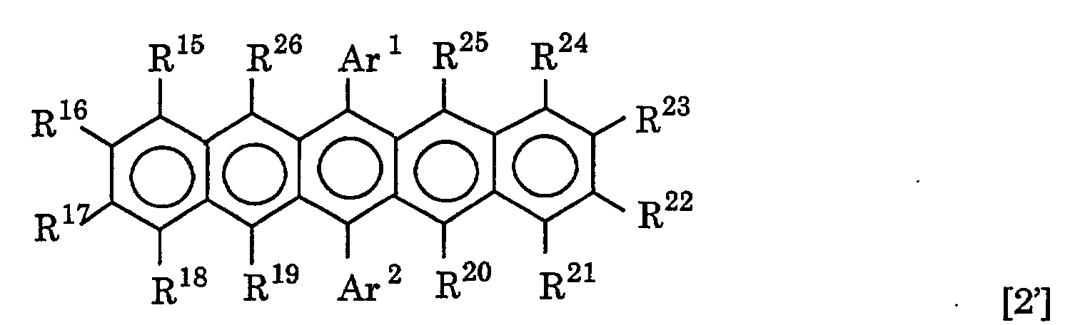
- An organic electroluminescence device according to Claim 1, wherein the organic layer comprises a light emitting layer which comprises the compound represented by general formula [1].
- An organic electroluminescence device according to Claim 2, wherein the organic layer comprises a light emitting layer which comprises the compound represented by general formula [2].
- An organic electroluminescence device according to Claim 4, wherein the light emitting layer comprises 0.1 to 20% by mole of the compound represented by general formula [1].
- An organic electroluminescence device according to Claim 5, wherein the light emitting layer comprises 0.1 to 20% by mole of the compound represented by general formula [2].
- An organic electroluminescence device according to any of Claims 4 to 7, wherein the light emitting layer has an electron transporting property.
- An organic electroluminescence device according to any of Claims 1, 2 and 4 to 8, wherein a layer of an inorganic compound is disposed between the organic layer and the electrode.
- An organic electroluminescence device according to any of Claims 1, 2 and 4 to 8, which emits reddish light.
Applications Claiming Priority (3)
| Application Number | Priority Date | Filing Date | Title |
|---|---|---|---|
| JP27946399A JP2001102172A (en) | 1999-09-30 | 1999-09-30 | Organic electroluminescent device |
| JP27946399 | 1999-09-30 | ||
| PCT/JP2000/006657 WO2001023496A1 (en) | 1999-09-30 | 2000-09-27 | Organic electroluminescent element |
Publications (2)
| Publication Number | Publication Date |
|---|---|
| EP1138744A1 true EP1138744A1 (en) | 2001-10-04 |
| EP1138744A4 EP1138744A4 (en) | 2006-06-28 |
Family
ID=17611426
Family Applications (1)
| Application Number | Title | Priority Date | Filing Date |
|---|---|---|---|
| EP00962881A Withdrawn EP1138744A4 (en) | 1999-09-30 | 2000-09-27 | Organic electroluminescent element |
Country Status (7)
| Country | Link |
|---|---|
| US (1) | US6489046B1 (en) |
| EP (1) | EP1138744A4 (en) |
| JP (1) | JP2001102172A (en) |
| KR (1) | KR20010093121A (en) |
| CN (1) | CN1174078C (en) |
| TW (1) | TW504942B (en) |
| WO (1) | WO2001023496A1 (en) |
Families Citing this family (32)
| Publication number | Priority date | Publication date | Assignee | Title |
|---|---|---|---|---|
| US7901594B2 (en) * | 2000-02-29 | 2011-03-08 | Japan Science And Technology Corporation | Polyacene derivatives and production thereof |
| JP4036682B2 (en) * | 2001-06-06 | 2008-01-23 | 三洋電機株式会社 | Organic electroluminescence device and light emitting material |
| JP4024526B2 (en) | 2001-08-29 | 2007-12-19 | 富士フイルム株式会社 | Fused octacyclic aromatic compound and organic EL device and organic EL display using the same |
| JP3804858B2 (en) | 2001-08-31 | 2006-08-02 | ソニー株式会社 | Organic electroluminescent device and manufacturing method thereof |
| US20030097010A1 (en) * | 2001-09-27 | 2003-05-22 | Vogel Dennis E. | Process for preparing pentacene derivatives |
| KR20040044998A (en) * | 2001-09-27 | 2004-05-31 | 쓰리엠 이노베이티브 프로퍼티즈 컴파니 | Substituted Pentacene Semiconductors |
| JP3953781B2 (en) | 2001-11-08 | 2007-08-08 | 富士フイルム株式会社 | Dinaphthopyrene compound and organic EL device and organic EL display using the same |
| US20030103022A1 (en) * | 2001-11-09 | 2003-06-05 | Yukihiro Noguchi | Display apparatus with function for initializing luminance data of optical element |
| JP2003186437A (en) * | 2001-12-18 | 2003-07-04 | Sanyo Electric Co Ltd | Display device |
| JP2003255899A (en) * | 2001-12-28 | 2003-09-10 | Sanyo Electric Co Ltd | Display device |
| JP3953330B2 (en) * | 2002-01-25 | 2007-08-08 | 三洋電機株式会社 | Display device |
| JP3723507B2 (en) * | 2002-01-29 | 2005-12-07 | 三洋電機株式会社 | Driving circuit |
| JP2003295825A (en) * | 2002-02-04 | 2003-10-15 | Sanyo Electric Co Ltd | Display device |
| JP3841695B2 (en) | 2002-02-06 | 2006-11-01 | 富士写真フイルム株式会社 | Organic EL element and organic EL display |
| JP2003308030A (en) * | 2002-02-18 | 2003-10-31 | Sanyo Electric Co Ltd | Display device |
| JP2003332058A (en) * | 2002-03-05 | 2003-11-21 | Sanyo Electric Co Ltd | Electroluminescence panel and its manufacturing method |
| JP2003258094A (en) * | 2002-03-05 | 2003-09-12 | Sanyo Electric Co Ltd | Wiring method, method forming the same, and display device |
| JP2003257645A (en) * | 2002-03-05 | 2003-09-12 | Sanyo Electric Co Ltd | Light emitting device and method of manufacturing the same |
| CN100517422C (en) * | 2002-03-07 | 2009-07-22 | 三洋电机株式会社 | Distributing structure, its manufacturing method and optical equipment |
| JP3671012B2 (en) * | 2002-03-07 | 2005-07-13 | 三洋電機株式会社 | Display device |
| JP3837344B2 (en) * | 2002-03-11 | 2006-10-25 | 三洋電機株式会社 | Optical element and manufacturing method thereof |
| JP3825344B2 (en) | 2002-03-15 | 2006-09-27 | 富士写真フイルム株式会社 | Organic EL element and organic EL display |
| JP4274374B2 (en) | 2003-01-30 | 2009-06-03 | 富士フイルム株式会社 | Hole injection layer material, organic EL element and organic EL display |
| US8030124B2 (en) * | 2004-11-05 | 2011-10-04 | Creator Technology B.V. | Method for patterning an organic material to concurrently form an insulator and a semiconductor and device formed thereby |
| JP2007013097A (en) * | 2005-06-01 | 2007-01-18 | Sony Corp | Organic semiconductor material, organic semiconductor thin film, and organic semiconductor element |
| CN100425599C (en) * | 2005-12-31 | 2008-10-15 | 清华大学 | Organic electroluminescent material and its application |
| JP5101055B2 (en) * | 2006-07-06 | 2012-12-19 | 双葉電子工業株式会社 | COMPOUND FOR ORGANIC EL ELEMENT AND ORGANIC EL ELEMENT |
| JP5478819B2 (en) * | 2007-11-02 | 2014-04-23 | キヤノン株式会社 | Fused polycyclic compound and organic light emitting device using the same |
| KR20090118324A (en) * | 2008-05-13 | 2009-11-18 | 주식회사 동진쎄미켐 | Method for preparing an intermediate of a blue light-emitting material using anthrone |
| KR20140089233A (en) | 2013-01-04 | 2014-07-14 | 삼성디스플레이 주식회사 | Fabricating method for the organic light emitting diode |
| PL3426232T3 (en) | 2016-03-09 | 2022-01-10 | Nls Pharmaceutics Ag | A mazindol ir/sr multilayer tablet and its use for the treatment of attention deficit/hyperactivity disorder (adhd) |
| CN106866348B (en) * | 2017-01-18 | 2018-12-18 | 中国科学院上海有机化学研究所 | A kind of polycyclic aromatic hydrocarbon compounds, synthetic method and purposes |
Citations (3)
| Publication number | Priority date | Publication date | Assignee | Title |
|---|---|---|---|---|
| EP0525739A1 (en) * | 1991-08-01 | 1993-02-03 | Eastman Kodak Company | Improved blue emitting internal junction organic electroluminescent device (I) |
| JPH08311442A (en) * | 1995-05-17 | 1996-11-26 | Tdk Corp | Organic el element |
| WO1998042655A1 (en) * | 1997-03-20 | 1998-10-01 | Aventis Research & Technologies Gmbh & Co Kg | Spiro compounds and the use thereof |
Family Cites Families (5)
| Publication number | Priority date | Publication date | Assignee | Title |
|---|---|---|---|---|
| JP3069139B2 (en) * | 1990-03-16 | 2000-07-24 | 旭化成工業株式会社 | Dispersion type electroluminescent device |
| JPH05214334A (en) * | 1992-02-05 | 1993-08-24 | Konica Corp | Organic thin-film electroluminescent element |
| JP3693128B2 (en) * | 1996-03-08 | 2005-09-07 | 出光興産株式会社 | Organic electroluminescence device |
| JP4278186B2 (en) * | 1997-05-15 | 2009-06-10 | 三洋電機株式会社 | Organic electroluminescence device |
| US6391482B1 (en) * | 1999-02-04 | 2002-05-21 | Matsushita Electric Industrial Co., Ltd. | Organic material for electroluminescent device and electroluminescent device using the same |
-
1999
- 1999-09-30 JP JP27946399A patent/JP2001102172A/en not_active Withdrawn
-
2000
- 2000-09-27 EP EP00962881A patent/EP1138744A4/en not_active Withdrawn
- 2000-09-27 WO PCT/JP2000/006657 patent/WO2001023496A1/en not_active Application Discontinuation
- 2000-09-27 CN CNB008021252A patent/CN1174078C/en not_active Expired - Fee Related
- 2000-09-27 KR KR1020017006680A patent/KR20010093121A/en not_active Application Discontinuation
- 2000-09-29 TW TW089120299A patent/TW504942B/en not_active IP Right Cessation
- 2000-09-29 US US09/675,200 patent/US6489046B1/en not_active Expired - Fee Related
Patent Citations (3)
| Publication number | Priority date | Publication date | Assignee | Title |
|---|---|---|---|---|
| EP0525739A1 (en) * | 1991-08-01 | 1993-02-03 | Eastman Kodak Company | Improved blue emitting internal junction organic electroluminescent device (I) |
| JPH08311442A (en) * | 1995-05-17 | 1996-11-26 | Tdk Corp | Organic el element |
| WO1998042655A1 (en) * | 1997-03-20 | 1998-10-01 | Aventis Research & Technologies Gmbh & Co Kg | Spiro compounds and the use thereof |
Non-Patent Citations (2)
| Title |
|---|
| PATENT ABSTRACTS OF JAPAN vol. 1997, no. 03, 31 March 1997 (1997-03-31) -& JP 08 311442 A (TDK CORP), 26 November 1996 (1996-11-26) -& US 6 203 933 B1 (NAKAYA KENJI ET AL) 20 March 2001 (2001-03-20) * |
| See also references of WO0123496A1 * |
Also Published As
| Publication number | Publication date |
|---|---|
| TW504942B (en) | 2002-10-01 |
| WO2001023496A1 (en) | 2001-04-05 |
| JP2001102172A (en) | 2001-04-13 |
| CN1327469A (en) | 2001-12-19 |
| KR20010093121A (en) | 2001-10-27 |
| EP1138744A4 (en) | 2006-06-28 |
| CN1174078C (en) | 2004-11-03 |
| US6489046B1 (en) | 2002-12-03 |
Similar Documents
| Publication | Publication Date | Title |
|---|---|---|
| US6489046B1 (en) | Organic electroluminescence device | |
| US7053255B2 (en) | Substituted diphenylanthracene compounds for organic electroluminescence devices | |
| US8178218B2 (en) | Material for organic electroluminescent device and organic electroluminescent device using same | |
| EP1138745B1 (en) | Organic electroluminescent element | |
| US6515182B2 (en) | Arylamine compound and organic electroluminescence device | |
| EP0786926B1 (en) | Light-emitting material for organo-electroluminescence device and organo-electroluminescence devive for which the light-emitting material is adapted | |
| EP0934992B1 (en) | Light-emitting material for organo-electroluminescence device and organic electroluminescence device | |
| JP4562884B2 (en) | Organic electroluminescence device | |
| KR100868144B1 (en) | Novel styryl compounds and organic electroluminescent devices | |
| JP3666086B2 (en) | Luminescent material for organic electroluminescence device and organic electroluminescence device using the same | |
| JP3924943B2 (en) | Organic electroluminescent device material and organic electroluminescent device using the same | |
| JP4521105B2 (en) | Novel hydrocarbon compounds and organic electroluminescence devices |
Legal Events
| Date | Code | Title | Description |
|---|---|---|---|
| PUAI | Public reference made under article 153(3) epc to a published international application that has entered the european phase |
Free format text: ORIGINAL CODE: 0009012 |
|
| 17P | Request for examination filed |
Effective date: 20010514 |
|
| AK | Designated contracting states |
Kind code of ref document: A1 Designated state(s): AT BE CH CY DE DK ES FI FR GB GR IE IT LI LU MC NL PT SE |
|
| RIN1 | Information on inventor provided before grant (corrected) |
Inventor name: KOGA, HIDETOSHI Inventor name: IKEDA, HIDETSUGU Inventor name: TAGAMI, SANAE Inventor name: YANAGISAWA, YOSHINORI |
|
| A4 | Supplementary search report drawn up and despatched |
Effective date: 20060531 |
|
| 17Q | First examination report despatched |
Effective date: 20060828 |
|
| STAA | Information on the status of an ep patent application or granted ep patent |
Free format text: STATUS: THE APPLICATION IS DEEMED TO BE WITHDRAWN |
|
| 18D | Application deemed to be withdrawn |
Effective date: 20070108 |