EP1560308B1 - Semiconductor laser and method of manufacturing the same - Google Patents
Semiconductor laser and method of manufacturing the same Download PDFInfo
- Publication number
- EP1560308B1 EP1560308B1 EP05008897A EP05008897A EP1560308B1 EP 1560308 B1 EP1560308 B1 EP 1560308B1 EP 05008897 A EP05008897 A EP 05008897A EP 05008897 A EP05008897 A EP 05008897A EP 1560308 B1 EP1560308 B1 EP 1560308B1
- Authority
- EP
- European Patent Office
- Prior art keywords
- layer
- optical waveguide
- semiconductor laser
- cladding layer
- thickness
- Prior art date
- Legal status (The legal status is an assumption and is not a legal conclusion. Google has not performed a legal analysis and makes no representation as to the accuracy of the status listed.)
- Expired - Lifetime
Links
Images


Classifications
-
- B—PERFORMING OPERATIONS; TRANSPORTING
- B82—NANOTECHNOLOGY
- B82Y—SPECIFIC USES OR APPLICATIONS OF NANOSTRUCTURES; MEASUREMENT OR ANALYSIS OF NANOSTRUCTURES; MANUFACTURE OR TREATMENT OF NANOSTRUCTURES
- B82Y20/00—Nanooptics, e.g. quantum optics or photonic crystals
-
- H—ELECTRICITY
- H01—ELECTRIC ELEMENTS
- H01S—DEVICES USING THE PROCESS OF LIGHT AMPLIFICATION BY STIMULATED EMISSION OF RADIATION [LASER] TO AMPLIFY OR GENERATE LIGHT; DEVICES USING STIMULATED EMISSION OF ELECTROMAGNETIC RADIATION IN WAVE RANGES OTHER THAN OPTICAL
- H01S5/00—Semiconductor lasers
- H01S5/20—Structure or shape of the semiconductor body to guide the optical wave ; Confining structures perpendicular to the optical axis, e.g. index or gain guiding, stripe geometry, broad area lasers, gain tailoring, transverse or lateral reflectors, special cladding structures, MQW barrier reflection layers
- H01S5/22—Structure or shape of the semiconductor body to guide the optical wave ; Confining structures perpendicular to the optical axis, e.g. index or gain guiding, stripe geometry, broad area lasers, gain tailoring, transverse or lateral reflectors, special cladding structures, MQW barrier reflection layers having a ridge or stripe structure
- H01S5/223—Buried stripe structure
- H01S5/2231—Buried stripe structure with inner confining structure only between the active layer and the upper electrode
-
- H—ELECTRICITY
- H01—ELECTRIC ELEMENTS
- H01S—DEVICES USING THE PROCESS OF LIGHT AMPLIFICATION BY STIMULATED EMISSION OF RADIATION [LASER] TO AMPLIFY OR GENERATE LIGHT; DEVICES USING STIMULATED EMISSION OF ELECTROMAGNETIC RADIATION IN WAVE RANGES OTHER THAN OPTICAL
- H01S5/00—Semiconductor lasers
- H01S5/30—Structure or shape of the active region; Materials used for the active region
- H01S5/34—Structure or shape of the active region; Materials used for the active region comprising quantum well or superlattice structures, e.g. single quantum well [SQW] lasers, multiple quantum well [MQW] lasers or graded index separate confinement heterostructure [GRINSCH] lasers
- H01S5/343—Structure or shape of the active region; Materials used for the active region comprising quantum well or superlattice structures, e.g. single quantum well [SQW] lasers, multiple quantum well [MQW] lasers or graded index separate confinement heterostructure [GRINSCH] lasers in AIIIBV compounds, e.g. AlGaAs-laser, InP-based laser
- H01S5/3434—Structure or shape of the active region; Materials used for the active region comprising quantum well or superlattice structures, e.g. single quantum well [SQW] lasers, multiple quantum well [MQW] lasers or graded index separate confinement heterostructure [GRINSCH] lasers in AIIIBV compounds, e.g. AlGaAs-laser, InP-based laser with a well layer comprising at least both As and P as V-compounds
-
- H—ELECTRICITY
- H01—ELECTRIC ELEMENTS
- H01S—DEVICES USING THE PROCESS OF LIGHT AMPLIFICATION BY STIMULATED EMISSION OF RADIATION [LASER] TO AMPLIFY OR GENERATE LIGHT; DEVICES USING STIMULATED EMISSION OF ELECTROMAGNETIC RADIATION IN WAVE RANGES OTHER THAN OPTICAL
- H01S5/00—Semiconductor lasers
- H01S5/20—Structure or shape of the semiconductor body to guide the optical wave ; Confining structures perpendicular to the optical axis, e.g. index or gain guiding, stripe geometry, broad area lasers, gain tailoring, transverse or lateral reflectors, special cladding structures, MQW barrier reflection layers
- H01S5/2004—Confining in the direction perpendicular to the layer structure
-
- H—ELECTRICITY
- H01—ELECTRIC ELEMENTS
- H01S—DEVICES USING THE PROCESS OF LIGHT AMPLIFICATION BY STIMULATED EMISSION OF RADIATION [LASER] TO AMPLIFY OR GENERATE LIGHT; DEVICES USING STIMULATED EMISSION OF ELECTROMAGNETIC RADIATION IN WAVE RANGES OTHER THAN OPTICAL
- H01S5/00—Semiconductor lasers
- H01S5/20—Structure or shape of the semiconductor body to guide the optical wave ; Confining structures perpendicular to the optical axis, e.g. index or gain guiding, stripe geometry, broad area lasers, gain tailoring, transverse or lateral reflectors, special cladding structures, MQW barrier reflection layers
- H01S5/22—Structure or shape of the semiconductor body to guide the optical wave ; Confining structures perpendicular to the optical axis, e.g. index or gain guiding, stripe geometry, broad area lasers, gain tailoring, transverse or lateral reflectors, special cladding structures, MQW barrier reflection layers having a ridge or stripe structure
- H01S5/2205—Structure or shape of the semiconductor body to guide the optical wave ; Confining structures perpendicular to the optical axis, e.g. index or gain guiding, stripe geometry, broad area lasers, gain tailoring, transverse or lateral reflectors, special cladding structures, MQW barrier reflection layers having a ridge or stripe structure comprising special burying or current confinement layers
- H01S5/2214—Structure or shape of the semiconductor body to guide the optical wave ; Confining structures perpendicular to the optical axis, e.g. index or gain guiding, stripe geometry, broad area lasers, gain tailoring, transverse or lateral reflectors, special cladding structures, MQW barrier reflection layers having a ridge or stripe structure comprising special burying or current confinement layers based on oxides or nitrides
-
- H—ELECTRICITY
- H01—ELECTRIC ELEMENTS
- H01S—DEVICES USING THE PROCESS OF LIGHT AMPLIFICATION BY STIMULATED EMISSION OF RADIATION [LASER] TO AMPLIFY OR GENERATE LIGHT; DEVICES USING STIMULATED EMISSION OF ELECTROMAGNETIC RADIATION IN WAVE RANGES OTHER THAN OPTICAL
- H01S5/00—Semiconductor lasers
- H01S5/30—Structure or shape of the active region; Materials used for the active region
- H01S5/32—Structure or shape of the active region; Materials used for the active region comprising PN junctions, e.g. hetero- or double- heterostructures
- H01S5/3211—Structure or shape of the active region; Materials used for the active region comprising PN junctions, e.g. hetero- or double- heterostructures characterised by special cladding layers, e.g. details on band-discontinuities
- H01S5/3213—Structure or shape of the active region; Materials used for the active region comprising PN junctions, e.g. hetero- or double- heterostructures characterised by special cladding layers, e.g. details on band-discontinuities asymmetric clading layers
-
- H—ELECTRICITY
- H01—ELECTRIC ELEMENTS
- H01S—DEVICES USING THE PROCESS OF LIGHT AMPLIFICATION BY STIMULATED EMISSION OF RADIATION [LASER] TO AMPLIFY OR GENERATE LIGHT; DEVICES USING STIMULATED EMISSION OF ELECTROMAGNETIC RADIATION IN WAVE RANGES OTHER THAN OPTICAL
- H01S5/00—Semiconductor lasers
- H01S5/30—Structure or shape of the active region; Materials used for the active region
- H01S5/32—Structure or shape of the active region; Materials used for the active region comprising PN junctions, e.g. hetero- or double- heterostructures
- H01S5/323—Structure or shape of the active region; Materials used for the active region comprising PN junctions, e.g. hetero- or double- heterostructures in AIIIBV compounds, e.g. AlGaAs-laser, InP-based laser
- H01S5/32308—Structure or shape of the active region; Materials used for the active region comprising PN junctions, e.g. hetero- or double- heterostructures in AIIIBV compounds, e.g. AlGaAs-laser, InP-based laser emitting light at a wavelength less than 900 nm
- H01S5/32333—Structure or shape of the active region; Materials used for the active region comprising PN junctions, e.g. hetero- or double- heterostructures in AIIIBV compounds, e.g. AlGaAs-laser, InP-based laser emitting light at a wavelength less than 900 nm based on InGaAsP
-
- H—ELECTRICITY
- H01—ELECTRIC ELEMENTS
- H01S—DEVICES USING THE PROCESS OF LIGHT AMPLIFICATION BY STIMULATED EMISSION OF RADIATION [LASER] TO AMPLIFY OR GENERATE LIGHT; DEVICES USING STIMULATED EMISSION OF ELECTROMAGNETIC RADIATION IN WAVE RANGES OTHER THAN OPTICAL
- H01S5/00—Semiconductor lasers
- H01S5/30—Structure or shape of the active region; Materials used for the active region
- H01S5/34—Structure or shape of the active region; Materials used for the active region comprising quantum well or superlattice structures, e.g. single quantum well [SQW] lasers, multiple quantum well [MQW] lasers or graded index separate confinement heterostructure [GRINSCH] lasers
- H01S5/3407—Structure or shape of the active region; Materials used for the active region comprising quantum well or superlattice structures, e.g. single quantum well [SQW] lasers, multiple quantum well [MQW] lasers or graded index separate confinement heterostructure [GRINSCH] lasers characterised by special barrier layers
-
- H—ELECTRICITY
- H01—ELECTRIC ELEMENTS
- H01S—DEVICES USING THE PROCESS OF LIGHT AMPLIFICATION BY STIMULATED EMISSION OF RADIATION [LASER] TO AMPLIFY OR GENERATE LIGHT; DEVICES USING STIMULATED EMISSION OF ELECTROMAGNETIC RADIATION IN WAVE RANGES OTHER THAN OPTICAL
- H01S5/00—Semiconductor lasers
- H01S5/30—Structure or shape of the active region; Materials used for the active region
- H01S5/34—Structure or shape of the active region; Materials used for the active region comprising quantum well or superlattice structures, e.g. single quantum well [SQW] lasers, multiple quantum well [MQW] lasers or graded index separate confinement heterostructure [GRINSCH] lasers
- H01S5/343—Structure or shape of the active region; Materials used for the active region comprising quantum well or superlattice structures, e.g. single quantum well [SQW] lasers, multiple quantum well [MQW] lasers or graded index separate confinement heterostructure [GRINSCH] lasers in AIIIBV compounds, e.g. AlGaAs-laser, InP-based laser
- H01S5/34346—Structure or shape of the active region; Materials used for the active region comprising quantum well or superlattice structures, e.g. single quantum well [SQW] lasers, multiple quantum well [MQW] lasers or graded index separate confinement heterostructure [GRINSCH] lasers in AIIIBV compounds, e.g. AlGaAs-laser, InP-based laser characterised by the materials of the barrier layers
- H01S5/3436—Structure or shape of the active region; Materials used for the active region comprising quantum well or superlattice structures, e.g. single quantum well [SQW] lasers, multiple quantum well [MQW] lasers or graded index separate confinement heterostructure [GRINSCH] lasers in AIIIBV compounds, e.g. AlGaAs-laser, InP-based laser characterised by the materials of the barrier layers based on InGa(Al)P
Definitions
- This invention relates to a semiconductor laser, and more particularly to a semiconductor laser having an active region which includes at least a quantum well layer and an optical waveguide layer and is of In x Ga 1-x As y P 1-y (0 ⁇ x ⁇ 1, 0 ⁇ y ⁇ 1).
- a semiconductor laser has come to be used in wider and wider fields. Especially a semiconductor laser which has an GaAs substrate and oscillates in 0.7 to 1.1 ⁇ m band has come to be used, as its output power increases, not only for an optical disc and a laser printer but also for a light source for pumping a solid state laser, a fiber amplifier and a fiber laser, a primary light source for generating a second harmonic, a light source for thermally recording an image on a heat-sensitive material, for instance, in printing, a light source for medical use, a light source for laser machining and laser soldering, and the like.
- the semiconductor laser can output high power.
- a single mode laser which is narrow in width those which are 500mW or more in the maximum light output and 150mW or more in the practical light output have been reported as, for instance, a light source for pumping a fiber amplifier oscillating, for instance, at 0.98 ⁇ m or 1.02 ⁇ m.
- the catastrophic optical damage (COD) when the oscillation wavelength is, for instance, 0.87 ⁇ m is 11.3W in the case of an element which is 100 ⁇ m in stripe width and is 16.5W in the case of an element which is 200 ⁇ m in stripe width. See “ Electronics Letters", vol.34, No.2, P.184 (1998), (S.O'Brien, H. Zhao and R. J. Lang ).
- the thickness of each InGaP cladding layer is 0.1 ⁇ m and the optical confinement factor ( ⁇ ) to the active layer quantum well for a laser beam is relatively large. Accordingly, when a device which was 50 ⁇ m in stripe width was aged under 500mW at 50° C in an APC (automatic power control) mode, deterioration rate of the drive current was relatively large and was 5x10 -5 h -1 in median. Further when a device which was 200 ⁇ m in stripe width was aged under 2000mW at 25° C in an APC mode, deterioration rate of the drive current was also 5x10 -5 h -1 in median.
- APC automatic power control
- Such high output power semiconductor lasers having a relatively wide stripe comes to stop oscillating when the drive current increases by about 5%. Accordingly the service life of the latter semiconductor laser is estimated at about 1000 hours in median, which is practically insufficient. Further since being of a gain waveguide type, the conventional semiconductor lasers are disadvantageous in that fundamental oscillation characteristics such as the current versus light output characteristics become unstable due to fluctuation in transverse mode.
- the cladding layer is formed of InGaAlP for the purpose of suppressing deterioration in temperature characteristics due to leakage of electrons into the p-type cladding layer, as disclosed in "reference 2".
- reference 2 only the gain waveguide type is mentioned and optimization for the refractive index waveguide type is not mentioned.
- the p-type InGaAlP is generally disadvantageous as compared with AlGaAs in that it is high in electric resistance and thermal resistance. Reliability when such a material is used has not been discussed.
- the active layer is exposed to atmosphere on a GaAs substrate during production of a refractive index waveguide type element, crystallizability on the surface thereof deteriorates and remarkable deterioration of the exposed part of the crystal interface due to non-emission recombination of carriers is generated.
- etching is carried out up to a portion immediately above the active layer.
- etching is carried out so that the upper cladding layer is left in a small thickness (about 0.1 to 0.3 ⁇ m) by controlling the etching time.
- an InGaP etching stop layer (about 1 to 5nm in thickness), which is lattice-matched with the GaAs substrate, into the upper cladding layer as shown in Figure 3 , it becomes feasible to stop etching of the AlGaAs at the InGaP etching stop layer in various etching methods.
- an InGaP layer inserted into a p-type AlGaAs cladding layer sometimes deteriorates crystallization, which results in increase in electric resistance and/or built-in voltage. This is supposed because As on the surface of the AlGaAs is substituted by P to form AlGaAsp on the crystal interface of AlGaAs and InGaP at the beginning of crystal growth.
- a semiconductor laser in accordance with the preamble of claim 1 is known from FUKUNAGA T ET AL: "HIGHLY RELIABLE OPERATIONS OF HIGH-POWER INGAASP/INGAP/ALGAAS 0.8 MU M SEPARATE CONFINEMENT HETEROSTRUCTURE LASERS" JAPANESE JOURNAL OF APPLIED PHYSICS, PUBLICATION OFFICE JAPANESE JOURNAL OF APPLIED PHYSICS. TOKYO, JP, vol. 34, no. 9B, 15 September 1995 (1995-09-15), pages L1175-L1177, XP000702502 ISSN: 0021-4922 . Specifically, this document discloses a gain-guided laser with a thickness of the waveguide of 0.1 ⁇ m.
- an object of the present invention is to provide a high power semiconductor laser in which the service-life elongating effect of using an Al-free active layer material is enhanced and the long-term reliability is improved.
- the semiconductor laser in accordance with the present invention comprises the features of claim 1.
- the light density ( ⁇ /d) in the quantum well portion is reduced by virtue of the optical waveguide layer not smaller than 0.25 ⁇ m in thickness, whereby internal loss is reduced and the deterioration rate in the drive current during APC aging which increases in proportion to the fourth or more power of the light density is reduced.
- the semiconductor laser of the present invention is a refractive index waveguide type element since a part of the upper cladding layer on the upper optical waveguide layer is selectively removed up to the interface of the upper cladding layer and the upper optical waveguide layer.
- the upper cladding layer is removed by etching inside or outside the stripe.
- removing by etching a part of the upper cladding layer conventionally, there is employed a method in which a part of the upper cladding layer is left unetched by providing an etching stop layer which differs from the upper cladding layer in composition and/or component atoms and is etched at a rate greatly smaller than the upper cladding layer ("reference 4"), or a method in which a part of the upper cladding layer is left unetched by controlling the etching time (See “reference 5": " Applied Physics Letters", Vol. 51, Bo. 10, p. 707 (1987), (T. Hayakawa, T. Suyama, K. Takahasi, M. Kondo, S. Yamamoto, and T. Hijikata )).
- the upper cladding layer is removed up to the optical waveguide layer having an increased thickness.
- an organic etching solution such as of sulfuric acid or citric acid, etching can be stopped at the optical waveguide layer.
- the cladding layer is left in a thickness of 0.1 to 0.2 ⁇ m in order to suppress deterioration in crystallization without deteriorating the quality of the active layer.
- the thickness of the optical waveguide layer is not smaller than 0.25 ⁇ m, deterioration in crystallization does not occur even if the cladding layer is removed to the optical waveguide layer.
- the distance between the quantum well in the active layer and the surface of the optical waveguide layer at the part where the cladding layer is removed is increased, damage to the active layer during formation of the refractive index waveguide structure can be suppressed.
- the service-life elongating effect of using an Al-free active layer material can be enhanced and the long-term reliability is greatly improved in accordance with the present invention.
- the semiconductor laser of the present invention has high quality properties as a refractive index waveguide type laser and, at the same time, is very small in variation of properties with time, it can improve system reliability when used as a light source for the field of image forming where noise and/or change in intensity and/or shape of the beam give rise to a problem.
- the semiconductor laser of the present invention can be applied, for instance, to a printing system where a semiconductor laser pumped solid state laser is employed, or to a visible or ultraviolet light source for a printer or an image scanner where a semiconductor laser pumped solid state laser is employed in combination with a SHG.
- a printer using heat-sensitive recording material where a semiconductor laser beam is used as a writing light beam
- the semiconductor lasers of the present invention greatly contribute to improvement of system reliability.
- the thickness of the optical waveguide layer reduces trailing of evanescent light oozing into the cladding layer and accordingly, the upper cladding layer can be reduced in thickness without adverse influence of absorption of the capping layer. Accordingly, the thickness of the upper cladding layer, which conventionally should be not smaller than 1.5 ⁇ m, may be reduced to not larger than 1 ⁇ m.
- the upper cladding layer is of such a small thickness, unevenness after etching which the refractive index waveguide structure inherently has can be small, which facilitates the subsequent lithography process and improves the accuracy of the lithography process. Further since the irregularity on the surface of a finished device is reduced, uniform wax wetting is obtained during chip bonding, which improves heat dissipation properties.
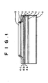
- a semiconductor laser in accordance with an example suitable for the understanding of the present invention comprises an n-GaAs buffer layer 2 (doped with 1x10 18 cm -3 Si, 0.5 ⁇ m thick), an n-Al 0.63 Ga 0.37 As lower cladding layer 3 (doped with 1x10 18 cm -3 Si, 1 ⁇ m thick), an undoped SCH active layer 4, a p-Al 0.63 Ga 0.37 As upper cladding layer 5 (doped with 1x10 18 cm -3 Zn, 1 ⁇ m thick), a p-GaAs capping layer 6 (doped with 2x10 19 cm -3 Zn, 0.3 ⁇ m thick), a SiO 2 insulating film 7 and a p-side electrode 8 formed one on another on one side of an n-GaAs substrate 1 (doped with 2x10 18 cm -3 Si) and an n-side electrode 9 formed on the other side of the substrate 1.
- the undoped SCH active layer 4 comprises an In 0.48 Ga 0.52 P lower optical waveguide layer 4a (undoped, 0.4 ⁇ m in thickness Wg), an In 0.13 Ga 0.87As0.75 P 0.25 quantum well layer 4b (undoped, 10nm thick) and an In 0.48 Ga 0.52 P upper optical waveguide layer 4c (undoped, 0.4 ⁇ m in thickness Wg).
- An n-GaAs buffer layer 2, an n-Al 0.63 Ga 0.37 As lower cladding layer 3, an undoped SCH active layer 4, a p-Al 0.63 Ga 0.37 As upper cladding layer 5 and a p-GaAs capping layer 6 are first formed one on another in this order on one side of an n-GaAs substrate 1 by low-pressure MOCVD.
- a mesa stripe structure which is 200 ⁇ m in bottom width is formed by photolithography and chemical etching by use of a 20:1:1 mixture of H 2 SO 4 , H 2 O 2 and H 2 O.
- the p-Al 0.63 Ga 0.37 As upper cladding layer 5 is etched at a rate 20-th or more as large as that at which the In 0.48 Ga 0.52 P upper optical waveguide layer 4c is etched.
- the mesa etching can be stopped just above the In 0.48 Ga 0.52 P upper optical waveguide layer 4c with good reproducibility.
- a SiO 2 insulating film 7 is formed by plasma CVD, and a part of the SiO 2 insulating film 7 on the upper surface of the mesa in a region within 1 to 5 ⁇ m from opposite edges of the mesa is etched and removed by photolithography and etching by use of dilute HF.
- a p-side electrode 8 (Ti/Pt/Au) is formed by deposition and heat treatment, and the bottom surface of the GaAs substrate 1 is polished to thin the GaAs substrate 1 to about 100 to 150 ⁇ m.
- an n-side electrode 9 (AuGe/Ni/Au) is formed by deposition and heat treatment.
- a laser bar which is 1.5mm in resonator length and about 1.5cm in length is cut out from the wafer by scribe with a diamond needle and cleavage, and the light radiating end face and the back end face are applied with optical coating films so that their reflectances are 20% and 95%, respectively. Finally the laser bar is cut into a plurality of laser chips by scribe with a diamond needle and cleavage. Each laser chip is fixed to a copper block by soldering the p-side electrode to the copper block by In solder.
- the semiconductor laser produced in this manner oscillates at about 809nm by a threshold current of 660 to 700mA and can operate at a high output power of not lower than 2W.
- Figure 5 shows change with time of the drive current for this laser when the laser is driven under 2W at 25° C in an APC mode. As can be seen from Figure 5 , the laser operates very stably.
- comparison semiconductor laser elements which were the same as the semiconductor laser of the example not covered by the invention except that the thickness Wg of the InGaP optical waveguide guide layer differed from that of the example were produced and their reliability was evaluated.
- Figures 6 to 8 show change with time of the drive current for the comparison lasers, which were 0.11 ⁇ m, 0.25 ⁇ m and an 0.6 ⁇ m in thickness Wg of the optical waveguide guide layer respectively, when the lasers were driven under 2W at 25° C in an APC mode.
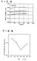
- Figure 9 shows the relation between the deterioration rate of the drive current (increase of drive current/drive current/time) in median and the thickness Wg of the optical waveguide layer in a stabilized state after the lasers are operated for 200 hours. As can be seen from Figure 9 , the deterioration rate of the drive current is very low.
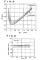
- Figure 4 shows calculated values of the relation between d/ ⁇ which is a value proportional to the reciprocal of the light density in the quantum well of the active layer of the structure in accordance with the present invention (d: thickness of the quantum well in ⁇ m, r: optical confinement factor to the active layer quantum well for a laser beam) and the thickness Wg of the optical waveguide layer.
- d thickness of the quantum well in ⁇ m
- r optical confinement factor to the active layer quantum well for a laser beam
- the thickness Wg was 0.6 ⁇ m
- the deterioration rate was larger than when the thickness Wg was 0.4 ⁇ m due to increase of the drive current by about 10%.
- the thickness Wg was not smaller than 0.25 ⁇ m, an excellent reliability was obtained, which proved that reliability was not deteriorated even if an insulated film such as SiO 2 was formed in contact with the optical waveguide layer without intervening therebetween an upper cladding layer left there in a small thickness as a protective layer as in the conventional semiconductor lasers shown in Figures 2 and 3 .
- current versus light out characteristics without kink could be obtained up to a high output range and both the far-field image and the near-field image were stable.
- the slope efficiency is proportional to the external differential quantum efficiency ( ⁇ d ) for the whole radiating light.
- the external differential quantum efficiency ⁇ d is expressed by the following formula (1).
- ⁇ i ln 1 R f ⁇ R r ⁇ i ⁇ L + ln 1 R f ⁇ R r
- ⁇ i the internal differential quantum efficiency
- R f the reflectance of the light radiating end face
- R r represents the reflectance of the rear end face
- L represents the length of the resonator.
- the slope efficiency is related to the external differential quantum efficiency ⁇ d as L f L f + L r ⁇ ⁇ d from the following relation between the amount of light radiated from the front end face L f and that radiated from the read end face L r .
- L f L r R r R f ⁇ 1 - R f 1 - R r
- ⁇ i 2cm -1
- the semiconductor laser in accordance with an embodiment of the present invention comprises an n-GaAs buffer layer 42 (doped with 1x10 18 cm -3 Si, 0.5 ⁇ m thick), an n-Al 0.55 Ga 0.45 As lower cladding layer 43 (doped with 1x10 18 cm -3 Si, 1 ⁇ m thick), an undoped SCH active layer 44, an n-Al 0.65 Ga 0.35 As current blocking layer 45 (doped with 1x10 18 cm -3 Si, 0.8 ⁇ m thick), an n-GaAs protective layer 46 (doped with 1x10 18 cm -3 Si, 0.01 ⁇ m thick), a p-Al 0.55 Ga 0.45 As upper cladding layer 47 (doped with 1x10 18 cm -3 Zn, 1 ⁇ m thick), a p-GaAs capping layer 48 (doped with 2x10 19 cm
- the undoped SCH active layer 44 comprises an In 0.48 Ga 0.52 P lower optical waveguide layer 44a (undoped, 0.25 ⁇ m in thickness Wg), an In 0.13 Ga 0.87As0.75 P 0.25 quantum well layer 44b (undoped, 10nm thick) and an In 0.48 Ga 0.52 P upper optical waveguide layer 44c (undoped, 0.25 ⁇ m in thickness Wg).
- the laser is produced by two-step low-pressure MOCVD. That is, an n-GaAs buffer layer 42, an n-Al 0.55 Ga 0.45 As lower cladding layer 43, an undoped SCH active layer 44, an n-Al 0.65 Ga 0.35 As current blocking layer 45 and an n-GaAs protective layer 46 are first grown one on another in this order on one side of an n-GaAs substrate 41 by low-pressure MOCVD.
- a mesa stripe channel which is 200 ⁇ m in bottom width is formed by photolithography and chemical etching by use of a 20:1:1 mixture of H 2 SO 4 , H 2 O 2 and H 2 O.
- the etching is stopped just above the In 0.48 Ga 0.52 P upper optical waveguide layer 44c since the undoped SCH active layer 44 comprises the In 0.48 Ga 0.52 P lower optical waveguide layer 44a (undoped, 0.25 ⁇ m in thickness Wg), the In 0.13 Ga 0.87As0.75 P 0.25 quantum well layer 44b (undoped, 10nm thick) and the In 0.48 Ga 0.52 P upper optical waveguide layer 44c.
- a p-Al 0.55 Ga 0.45 As upper cladding layer 47 and a p-GaAs capping layer 48 are grown in sequence by low-pressure MOCVD.
- a p-side electrode 49 is formed, the GaAs substrate 41 is polished, an n-side electrode 50 is formed, a laser bar is cut out, the light radiating end face and the back end face are applied with optical coating films, and the laser bar is cut into a plurality of laser chips in the manner similar to that in the first embodiment.
- the semiconductor laser in accordance with the second embodiment of the present invention comprises an n-GaAs buffer layer 62 (doped with 1x10 18 cm -3 Si, 0.5 ⁇ m thick), an n-Al 0.6 Ga 0.4 As lower cladding layer 63 (doped with 1x10 18 cm -3 Si, 1 ⁇ m thick), an undoped SCH active layer 64, an n-Al 0.65 Ga 0.35 As current blocking layer 66 (doped with 1x10 18 cm -3 Si, 0.8 ⁇ m thick), a p-GaAs protective layer 67 (doped with 1x10 18 cm -3 Si, 0.01 ⁇ m thick), a p-Al 0.6 Ga 0.4 As first upper cladding layer 65 (doped with 1x10 18 cm -3 Zn, 1 ⁇ m thick), a p-Al 0.6 Ga 0.4 As second upper
- the undoped SCH active layer 64 comprises an In 0.48 Ga 0.52 P lower optical waveguide layer 64a (undoped, 0.25 ⁇ m in thickness Wg), an In 0.13 Ga 0.87As0.75 P 0.25 quantum well layer 64b (undoped, 10nm thick) and an In 0.48 Ga 0.52 P upper optical waveguide layer 64c (undoped, 0.25 ⁇ m in thickness Wg).
- the laser is produced by three-step low-pressure MOCVD. That is, an n-GaAs buffer layer 62, an n-Al 0.55 Ga 0.45 As lower cladding layer 63, an undoped SCH active layer 64, a pAl 0.6 Ga 0.4 As first upper cladding layer 65 and a p-GaAs protective layer 67 are grown one on another in this order on one side of an n-GaAs substrate 41 by first low-pressure MOCVD.
- a SiO 2 film 0.25 ⁇ m thick is formed by plasma CVD, and a stripe-like SiO 2 mask 200 ⁇ m wide is formed by photolithography and etching by use of dilute HF.
- n-Al 0.65 Ga 0.35 As current blocking layer 66 and a p-GaAs protective layer 67 are grown by second low-pressure MOCVD. At this time, though polycrystal grows also on the SiO 2 mask, it can be removed by next etching. Then short etching by use of a mixture of H 2 SO 4 , H 2 O 2 and H 2 O is carried out and the SiO 2 mask is removed by dilute HF.
- a pAl 0.6 Ga 0.4 As second upper cladding layer 68 and a p-GaAs capping layer 69 are grown by third low-pressure MOCVD.
- a p-side electrode 70 is formed, the GaAs substrate 61 is polished, an n-side electrode 71 is formed, a laser bar is cut out, the light radiating end face and the back end face are applied with optical coating films, and the laser bar is cut into a plurality of laser chips in the manner similar to that in the first embodiment.
- the present invention is described above in conjunction with a broad stripe semiconductor laser having a stripe 200 ⁇ m wide, the present invention can also be applied to multiple transverse mode semiconductor lasers having a broad stripe of various widths or a single transverse mode semiconductor lasers which are not larger than about 6 ⁇ m in width of the stripe.
- the active layer which includes at least a quantum well layer and upper and lower optical waveguide layers has only to be of In x Ga 1-x As y P 1-y (0 ⁇ x ⁇ 1, 0 ⁇ y ⁇ 1), and a strain layer which is not lattice-matched with the substrate may be partly used. Further the upper and lower optical waveguide layers on opposite sides of the quantum well layer may be of different thicknesses. In this case, the quantum well layer is shifted from a position in which the light intensity is maximized and the optical confinement factor r is reduced, and accordingly, the light density in the quantum well can be reduced when the thicker one of the optical waveguide layers is not smaller than 0.25 ⁇ m.
Description
- This invention relates to a semiconductor laser, and more particularly to a semiconductor laser having an active region which includes at least a quantum well layer and an optical waveguide layer and is of InxGa1-xAsyP1-y (0≦x≦1, 0≦y≦1).
- A semiconductor laser has come to be used in wider and wider fields. Especially a semiconductor laser which has an GaAs substrate and oscillates in 0.7 to 1.1µm band has come to be used, as its output power increases, not only for an optical disc and a laser printer but also for a light source for pumping a solid state laser, a fiber amplifier and a fiber laser, a primary light source for generating a second harmonic, a light source for thermally recording an image on a heat-sensitive material, for instance, in printing, a light source for medical use, a light source for laser machining and laser soldering, and the like.
- In these applications, it is extremely important that the semiconductor laser can output high power. In a single mode laser which is narrow in width (not larger than about 5µm), those which are 500mW or more in the maximum light output and 150mW or more in the practical light output have been reported as, for instance, a light source for pumping a fiber amplifier oscillating, for instance, at 0.98µm or 1.02µm. Further it has been reported that, in multiple-mode lasers which are about 50µm or more in stripe width, the catastrophic optical damage (COD) when the oscillation wavelength is, for instance, 0.87µm is 11.3W in the case of an element which is 100µm in stripe width and is 16.5W in the case of an element which is 200µm in stripe width. See "Electronics Letters", vol.34, No.2, P.184 (1998), (S.O'Brien, H. Zhao and R. J. Lang).
- These inventors have proposed a semiconductor laser in which catastrophic failure due to oxidization of Al is prevented by freeing the vicinity of the light emission region (a quantum well layer and an optical waveguide layer which is adjacent to the quantum well layer and forms a barrier) from Al and at the same time, an AlGaAs layer is employed as a cladding layer in order to prevent deterioration in temperature characteristics due to leakage of electrons from the active region. With this arrangement, the semiconductor laser can operate at high output power. See "Japanese Journal of Applied Physics", Vol. 34, No. 9B, p. L1175 (1995), (T. Fukunaga, M. Wada, H. Asano and T. Hauakawa). This will be referred to as "reference 1", hereinbelow.
- In the semiconductor laser which these inventors have proposed, the thickness of each InGaP cladding layer is 0.1µm and the optical confinement factor (Γ) to the active layer quantum well for a laser beam is relatively large. Accordingly, when a device which was 50µm in stripe width was aged under 500mW at 50° C in an APC (automatic power control) mode, deterioration rate of the drive current was relatively large and was 5x10⁻⁵h-1 in median. Further when a device which was 200µm in stripe width was aged under 2000mW at 25° C in an APC mode, deterioration rate of the drive current was also 5x10⁻⁵ h-1 in median.
- Such high output power semiconductor lasers having a relatively wide stripe comes to stop oscillating when the drive current increases by about 5%. Accordingly the service life of the latter semiconductor laser is estimated at about 1000 hours in median, which is practically insufficient. Further since being of a gain waveguide type, the conventional semiconductor lasers are disadvantageous in that fundamental oscillation characteristics such as the current versus light output characteristics become unstable due to fluctuation in transverse mode.
- Further there has been known a semiconductor laser in which the output power is increased by employing Al-free material different from that disclosed in "reference 1" and at the same time reducing the optical confinement factor (Γ) to the active layer quantum well for a laser beam by increasing the thickness of the optical waveguide layer. See "Appl. Phys. Lett.", Vol. 72, No.1, P. 4, (J.K. Wade, L. J. Mawst, D. Botez. R.F. Nabiev, M. Jansen and L. A. Morris) (reference 2) and "SPIE Proceeding", Vol. 3001, p. 2 (1997), (M.A. Emanuel, J. A. Skidnore and R. J. Beach) (reference 3).
- However, as disclosed in "reference 1", especially in the wavelength range not longer than 850nm, temperature characteristics deteriorate due to leakage of electrons into a p-type cladding layer when the cladding layer is formed of a material free from Al. This is because electron barrier cannot be sufficient even if InGaP is used which is the largest in forbidden band width in materials which can be lattice-matched with the GaAs substrate.
- Further when producing such a refractive index waveguide type element, it is difficult to stop etching at the interface of an InGaP cladding layer and an InGaAsP optical waveguide layer since these layers resemble each other in chemical properties.
- Further there has been reported an element in which the cladding layer is formed of InGaAlP for the purpose of suppressing deterioration in temperature characteristics due to leakage of electrons into the p-type cladding layer, as disclosed in "reference 2". However in "reference 2", only the gain waveguide type is mentioned and optimization for the refractive index waveguide type is not mentioned.
- Further, the p-type InGaAlP is generally disadvantageous as compared with AlGaAs in that it is high in electric resistance and thermal resistance. Reliability when such a material is used has not been discussed. When the active layer is exposed to atmosphere on a GaAs substrate during production of a refractive index waveguide type element, crystallizability on the surface thereof deteriorates and remarkable deterioration of the exposed part of the crystal interface due to non-emission recombination of carriers is generated.
- Accordingly, a method in which etching is carried out up to a portion immediately above the active layer has been generally employed. In this case, as in a ridge waveguide type laser shown in
Figure 2 , etching is carried out so that the upper cladding layer is left in a small thickness (about 0.1 to 0.3µm) by controlling the etching time. - However such etching time control is disadvantageous in that reproducibility deteriorates due to fluctuation in etching conditions and thickness of the cladding layer from wafer to wafer. In order to overcome this problem, there has been proposed a structure in which an etching stop layer is inserted as shown in
Figure 3 . SeeUnited States Patent No. 4,567,060 (reference 4). - For example, in the case where an AlGaAs cladding layer and an InGaAsP active region are combined, by inserting an InGaP etching stop layer (about 1 to 5nm in thickness), which is lattice-matched with the GaAs substrate, into the upper cladding layer as shown in
Figure 3 , it becomes feasible to stop etching of the AlGaAs at the InGaP etching stop layer in various etching methods. - However an InGaP layer inserted into a p-type AlGaAs cladding layer sometimes deteriorates crystallization, which results in increase in electric resistance and/or built-in voltage. This is supposed because As on the surface of the AlGaAs is substituted by P to form AlGaAsp on the crystal interface of AlGaAs and InGaP at the beginning of crystal growth.
- A semiconductor laser in accordance with the preamble of claim 1 is known from FUKUNAGA T ET AL: "HIGHLY RELIABLE OPERATIONS OF HIGH-POWER INGAASP/INGAP/ALGAAS 0.8 MU M SEPARATE CONFINEMENT HETEROSTRUCTURE LASERS" JAPANESE JOURNAL OF APPLIED PHYSICS, PUBLICATION OFFICE JAPANESE JOURNAL OF APPLIED PHYSICS. TOKYO, JP, vol. 34, no. 9B, 15 September 1995 (1995-09-15), pages L1175-L1177, XP000702502 ISSN: 0021-4922. Specifically, this document discloses a gain-guided laser with a thickness of the waveguide of 0.1 µm.
- In view of the foregoing observations and description, an object of the present invention is to provide a high power semiconductor laser in which the service-life elongating effect of using an Al-free active layer material is enhanced and the long-term reliability is improved.
- The semiconductor laser in accordance with the present invention comprises the features of claim 1.
- In the semiconductor laser of the present invention, the light density (Γ/d) in the quantum well portion is reduced by virtue of the optical waveguide layer not smaller than 0.25µm in thickness, whereby internal loss is reduced and the deterioration rate in the drive current during APC aging which increases in proportion to the fourth or more power of the light density is reduced.
- The semiconductor laser of the present invention is a refractive index waveguide type element since a part of the upper cladding layer on the upper optical waveguide layer is selectively removed up to the interface of the upper cladding layer and the upper optical waveguide layer.
- When such a refractive index waveguide type element structure, the upper cladding layer is removed by etching inside or outside the stripe. When removing by etching a part of the upper cladding layer, conventionally, there is employed a method in which a part of the upper cladding layer is left unetched by providing an etching stop layer which differs from the upper cladding layer in composition and/or component atoms and is etched at a rate greatly smaller than the upper cladding layer ("reference 4"), or a method in which a part of the upper cladding layer is left unetched by controlling the etching time (See "reference 5": "Applied Physics Letters", Vol. 51, Bo. 10, p. 707 (1987), (T. Hayakawa, T. Suyama, K. Takahasi, M. Kondo, S. Yamamoto, and T. Hijikata)).
- To the contrast, in accordance with the method of the present invention, the upper cladding layer is removed up to the optical waveguide layer having an increased thickness. By using an organic etching solution such as of sulfuric acid or citric acid, etching can be stopped at the optical waveguide layer. By stopping etching without use of an etching stop layer which adversely affects properties of the elements, the refractive index waveguide structure can be produced with good reproducibility, whereby fundamental oscillation characteristics can be stabilized.
- Conventionally since the optical waveguide layer is small in thickness, i.e., about 0.1µm, the cladding layer is left in a thickness of 0.1 to 0.2µm in order to suppress deterioration in crystallization without deteriorating the quality of the active layer. However, when the thickness of the optical waveguide layer is not smaller than 0.25µm, deterioration in crystallization does not occur even if the cladding layer is removed to the optical waveguide layer.
- Further in the method of the present invention, since the distance between the quantum well in the active layer and the surface of the optical waveguide layer at the part where the cladding layer is removed is increased, damage to the active layer during formation of the refractive index waveguide structure can be suppressed.
- As can be understood from the description above, the service-life elongating effect of using an Al-free active layer material can be enhanced and the long-term reliability is greatly improved in accordance with the present invention. Especially, since the semiconductor laser of the present invention has high quality properties as a refractive index waveguide type laser and, at the same time, is very small in variation of properties with time, it can improve system reliability when used as a light source for the field of image forming where noise and/or change in intensity and/or shape of the beam give rise to a problem.
- As application to the field of image forming, the semiconductor laser of the present invention can be applied, for instance, to a printing system where a semiconductor laser pumped solid state laser is employed, or to a visible or ultraviolet light source for a printer or an image scanner where a semiconductor laser pumped solid state laser is employed in combination with a SHG. In the field of a printer using heat-sensitive recording material where a semiconductor laser beam is used as a writing light beam, several to about one hundred high power semiconductor lasers are used in one system, and accordingly, the semiconductor lasers of the present invention greatly contribute to improvement of system reliability.
- Further in the semiconductor laser of the present invention, increase of the thickness of the optical waveguide layer reduces trailing of evanescent light oozing into the cladding layer and accordingly, the upper cladding layer can be reduced in thickness without adverse influence of absorption of the capping layer. Accordingly, the thickness of the upper cladding layer, which conventionally should be not smaller than 1.5µm, may be reduced to not larger than 1µm. When the upper cladding layer is of such a small thickness, unevenness after etching which the refractive index waveguide structure inherently has can be small, which facilitates the subsequent lithography process and improves the accuracy of the lithography process. Further since the irregularity on the surface of a finished device is reduced, uniform wax wetting is obtained during chip bonding, which improves heat dissipation properties.
-
-
Figure 1 is a schematic view showing the layer arrangement of a ridge waveguide type semiconductor laser in accordance with an example not covered by the present invention, -
Figure 2 is a schematic view showing the layer arrangement of an example of a conventional ridge waveguide type semiconductor laser, -
Figure 3 is a schematic view showing the layer arrangement of another example of a conventional ridge waveguide type semiconductor laser, -
Figure 4 is a view showing the dependency on the thickness of the optical waveguide layer of d/r which is a value proportional to the reciprocal of the light density in the quantum well, -
Figure 5 is a view showing change with time of the drive current for a ridge waveguide type semiconductor laser in accordance with the present invention where the optical waveguide layer is 0.4µm in thickness, -
Figure 6 is a view showing change with time of the drive current for a conventional ridge waveguide type semiconductor laser, -
Figure 7 is a view showing change with time of the drive current for a ridge waveguide type semiconductor laser in accordance with an example not covered by the present invention where the optical waveguide layer is 0.25µm in thickness, -
Figure 8 is a view showing change with time of the drive current for a ridge waveguide type semiconductor laser in accordance with an example not covered by the present invention where the optical waveguide layer is 0.6µm in thickness, -
Figure 9 is a view showing the dependency on the thickness of the optical waveguide layer of the drive current deterioration rate in a ridge waveguide type semiconductor laser, -
Figure 10 is a view showing the dependency on the thickness of the optical waveguide layer of the catastrophic optical damage of a ridge waveguide type semiconductor laser, -
Figure 11 is a view showing the relation between the drive current deterioration rate and the internal light power in a conventional ridge waveguide type semiconductor laser, -
Figure 12 is a view showing comparison of measured values of catastrophic optical damage (COD) and the calculated value of internal light power at the front end face of a conventional ridge waveguide type semiconductor laser for various reflectances of the coating applied to the front end face, -
Figure 13 is a view showing comparison of measured relation between the number of quantum wells and the slop efficiency and theoretical relation of the same, -
Figure 14 is a view showing measured values and calculated values of dependency on the thickness of the optical waveguide layer of the slope efficiency of a single quantum well semiconductor laser and a double quantum well semiconductor laser, -
Figure 15 is a view showing the current versus light output characteristics of a ridge waveguide type semiconductor laser, -
Figure 16 is a schematic view showing the layer arrangement of a ridge waveguide type semiconductor laser in accordance with a first embodiment of the present invention, and -
Figure 17 is a schematic view showing the layer arrangement of a ridge waveguide type semiconductor laser in accordance with a second embodiment of the present invention. - In
Figure 1 , a semiconductor laser in accordance with an example suitable for the understanding of the present invention comprises an n-GaAs buffer layer 2 (doped with 1x1018cm-3 Si, 0.5µm thick), an n-Al0.63Ga0.37As lower cladding layer 3 (doped with 1x1018cm-3 Si, 1µm thick), an undoped SCH active layer 4, a p-Al0.63Ga0.37As upper cladding layer 5 (doped with 1x1018cm-3 Zn, 1µm thick), a p-GaAs capping layer 6 (doped with 2x1019cm-3 Zn, 0.3µm thick), a SiO2 insulating film 7 and a p-side electrode 8 formed one on another on one side of an n-GaAs substrate 1 (doped with 2x1018cm-3 Si) and an n-side electrode 9 formed on the other side of the substrate 1. - The undoped SCH active layer 4 comprises an In0.48Ga0.52P lower optical waveguide layer 4a (undoped, 0.4µm in thickness Wg), an In0.13Ga0.87As0.75P0.25 quantum well layer 4b (undoped, 10nm thick) and an In0.48Ga0.52P upper optical waveguide layer 4c (undoped, 0.4µm in thickness Wg).
- A method manufacturing this semiconductor laser will be described, hereinbelow. An n-GaAs buffer layer 2, an n-Al0.63Ga0.37As lower cladding layer 3, an undoped SCH active layer 4, a p-Al0.63Ga0.37As upper cladding layer 5 and a p-GaAs capping layer 6 are first formed one on another in this order on one side of an n-GaAs substrate 1 by low-pressure MOCVD.
- Then a mesa stripe structure which is 200µm in bottom width is formed by photolithography and chemical etching by use of a 20:1:1 mixture of H2SO4, H2O2 and H2O. At this time, the p-Al0.63Ga0.37As upper cladding layer 5 is etched at a rate 20-th or more as large as that at which the In0.48Ga0.52P upper optical waveguide layer 4c is etched. By virtue of this fact, the mesa etching can be stopped just above the In0.48Ga0.52P upper optical waveguide layer 4c with good reproducibility.
- Thereafter, a SiO2 insulating film 7 is formed by plasma CVD, and a part of the SiO2 insulating film 7 on the upper surface of the mesa in a region within 1 to 5µm from opposite edges of the mesa is etched and removed by photolithography and etching by use of dilute HF.
- Then a p-side electrode 8 (Ti/Pt/Au) is formed by deposition and heat treatment, and the bottom surface of the GaAs substrate 1 is polished to thin the GaAs substrate 1 to about 100 to 150µm. Finally an n-side electrode 9 (AuGe/Ni/Au) is formed by deposition and heat treatment.
- A laser bar which is 1.5mm in resonator length and about 1.5cm in length is cut out from the wafer by scribe with a diamond needle and cleavage, and the light radiating end face and the back end face are applied with optical coating films so that their reflectances are 20% and 95%, respectively. Finally the laser bar is cut into a plurality of laser chips by scribe with a diamond needle and cleavage. Each laser chip is fixed to a copper block by soldering the p-side electrode to the copper block by In solder.
- The semiconductor laser produced in this manner oscillates at about 809nm by a threshold current of 660 to 700mA and can operate at a high output power of not lower than 2W.
Figure 5 shows change with time of the drive current for this laser when the laser is driven under 2W at 25° C in an APC mode. As can be seen fromFigure 5 , the laser operates very stably. - In a first experiment, comparison semiconductor laser elements which were the same as the semiconductor laser of the example not covered by the invention except that the thickness Wg of the InGaP optical waveguide guide layer differed from that of the example were produced and their reliability was evaluated.
Figures 6 to 8 show change with time of the drive current for the comparison lasers, which were 0.11µm, 0.25µm and an 0.6µm in thickness Wg of the optical waveguide guide layer respectively, when the lasers were driven under 2W at 25° C in an APC mode. As can be seen fromFigures 6 to 8 , when the thickness Wg of the optical waveguide guide layer was smaller than 0.25µm, deterioration of the drive current was large (Figure 6 ), while when the thickness Wg of the optical waveguide guide layer was not smaller than 0.25µm, deterioration of the drive current was relatively small and the lasers operated stably (Figures 7 and8 ). -
Figure 9 shows the relation between the deterioration rate of the drive current (increase of drive current/drive current/time) in median and the thickness Wg of the optical waveguide layer in a stabilized state after the lasers are operated for 200 hours. As can be seen fromFigure 9 , the deterioration rate of the drive current is very low. -
Figure 4 shows calculated values of the relation between d/Γ which is a value proportional to the reciprocal of the light density in the quantum well of the active layer of the structure in accordance with the present invention (d: thickness of the quantum well in µm, r: optical confinement factor to the active layer quantum well for a laser beam) and the thickness Wg of the optical waveguide layer. As can be seen fromFigure 4 , when the thickness Wg of the optical waveguide layer was in the range of not smaller than 0.25µm, the light density in the quantum well decreased monotonically with increase of the thickness Wg of the optical waveguide layer, which proved improvement in reliability. - When the thickness Wg was 0.6µm, the deterioration rate was larger than when the thickness Wg was 0.4µm due to increase of the drive current by about 10%. Further when the thickness Wg was not smaller than 0.25µm, an excellent reliability was obtained, which proved that reliability was not deteriorated even if an insulated film such as SiO2 was formed in contact with the optical waveguide layer without intervening therebetween an upper cladding layer left there in a small thickness as a protective layer as in the conventional semiconductor lasers shown in
Figures 2 and3 . Further as shown inFigure 15 , current versus light out characteristics without kink could be obtained up to a high output range and both the far-field image and the near-field image were stable. - In a second experiment, the catastrophic optical damages of the aforesaid laser elements were measured. As shown in
Figure 10 , the catastrophic optical damage hardly changed with change of the thickness Wg of the optical waveguide layer. This proves that with the arrangement of the present invention, the catastrophic optical damage does not increase with increase of the thickness Wg of the optical waveguide layer as in the example disclosed in "reference 2", that is, the catastrophic optical damage is independent from the light density in the active layer. - In a third experiment, three kinds of laser elements which were the same as the conventional element shown in
Figure 6 in structure, were 0.11µm in thickness Wg of the optical waveguide layer and were respectively 11%, 20% and 30% in reflectance Rf of the light radiating end face were prepared and compared. - The relation between the drive current deterioration rate in median and the internal light density at the light radiating end face when the laser was driven under 1.8W at 25° C in an APC mode was measured for each laser. As can be seen from
Figure 11 , the drive current deterioration rate greatly increases substantially in proportion to the fourth power of the internal light density at the light radiating end face and greatly depends upon the whole internal light intensity. - In a fourth experiment, Rf dependency of the catastrophic optical damage was evaluated for laser elements which were 0.11µm in the thickness Wg of the optical waveguide layer. As shown in
Figure 12 , the catastrophic optical damage was proportional to the internal light power. - As a fifth example, factors which governed the internal loss (αi[cm-1]) were investigated on the basis of the slope efficiency for various laser elements. The experiment was carried out by use of laser elements having an oxide film stripe structure of 50µm width for the purpose of material evaluation.
Figure 13 shows the dependency of the slope efficiency on the number of the quantum wells Nw (Nw=1~4) with the total thickness of the active layer (including quantum wells (10nm wide), barrier layers (undoped InGaP the same as that of the optical waveguide layers, 10nm thick) parting the quantum wells and optical waveguide layers) fixed to 0.23µm. - The slope efficiency is proportional to the external differential quantum efficiency (ηd) for the whole radiating light. The external differential quantum efficiency ηd is expressed by the following formula (1).


Figure 13 were obtained letting ηi=0.7 (constant) and αi=Nwx2(cm-1) and well conform to the result of the experiment. Accordingly, the residual loss in the semiconductor laser of the example may be considered to be mainly governed by loss by the quantum wells themselves.' - Further single quantum well laser elements (Nw=1) and double quantum well laser elements (Nw=2) which were different from each other in the thickness Wg of the optical waveguide layer were prepared and the slope efficiency of each laser element was measured. As shown in
Figure 14 , the result of the measurement conformed to the calculated values in tendency that the internal loss increased in proportion to the amount of light in the quantum well. This supports that the residual loss in the semiconductor laser of the example is mainly governed by loss by the quantum wells themselves. - The result of the experiments shows that in the semiconductor lasers in accordance with the example, the deterioration mechanism and the internal loss are due to the inside of the active layer and greatly depend upon the light power in the active layer. Accordingly, these factors can be improved by making the thickness Wg of the optical waveguide layer not smaller than 0.25µm.
- A semiconductor laser in accordance with an embodiment of the present invention will be described with reference to
Figure 16 , hereinbelow. InFigure 16 , the semiconductor laser in accordance with an embodiment of the present invention comprises an n-GaAs buffer layer 42 (doped with 1x1018cm-3 Si, 0.5µm thick), an n-Al0.55Ga0.45As lower cladding layer 43 (doped with 1x1018cm-3 Si, 1µm thick), an undoped SCH active layer 44, an n-Al0.65Ga0.35As current blocking layer 45 (doped with 1x1018cm-3 Si, 0.8µm thick), an n-GaAs protective layer 46 (doped with 1x1018cm-3 Si, 0.01µm thick), a p-Al0.55Ga0.45As upper cladding layer 47 (doped with 1x1018cm-3 Zn, 1µm thick), a p-GaAs capping layer 48 (doped with 2x1019 cm-3 Zn, 0.3µm thick), and a p-side electrode 49 formed one on another on one side of an n-GaAs substrate 41 (doped with 2x1018 cm-3 Si) and an n-side electrode 50 formed on the other side of the substrate 41. - The undoped SCH active layer 44 comprises an In0.48Ga0.52P lower optical waveguide layer 44a (undoped, 0.25µm in thickness Wg), an In0.13Ga0.87As0.75P0.25 quantum well layer 44b (undoped, 10nm thick) and an In0.48Ga0.52P upper optical waveguide layer 44c (undoped, 0.25µm in thickness Wg).
- A method manufacturing this semiconductor laser will be described, hereinbelow. In this embodiment, unlike in the above example, the laser is produced by two-step low-pressure MOCVD. That is, an n-GaAs buffer layer 42, an n-Al0.55Ga0.45As lower cladding layer 43, an undoped SCH active layer 44, an n-Al0.65Ga0.35As current blocking layer 45 and an n-GaAs protective layer 46 are first grown one on another in this order on one side of an n-GaAs substrate 41 by low-pressure MOCVD.
- Then a mesa stripe channel which is 200µm in bottom width is formed by photolithography and chemical etching by use of a 20:1:1 mixture of H2SO4, H2O2 and H2O. At this time, the etching is stopped just above the In0.48Ga0.52P upper optical waveguide layer 44c since the undoped SCH active layer 44 comprises the In0.48Ga0.52P lower optical waveguide layer 44a (undoped, 0.25µm in thickness Wg), the In0.13Ga0.87As0.75P0.25 quantum well layer 44b (undoped, 10nm thick) and the In0.48Ga0.52P upper optical waveguide layer 44c.
- Then a p-Al0.55Ga0.45As upper cladding layer 47 and a p-GaAs capping layer 48 are grown in sequence by low-pressure MOCVD.
- Thereafter, a p-side electrode 49 is formed, the GaAs substrate 41 is polished, an n-side electrode 50 is formed, a laser bar is cut out, the light radiating end face and the back end face are applied with optical coating films, and the laser bar is cut into a plurality of laser chips in the manner similar to that in the first embodiment.
- A semiconductor laser in accordance with a second embodiment of the present invention will be described with reference to
Figure 17 , hereinbelow. InFigure 17 , the semiconductor laser in accordance with the second embodiment of the present invention comprises an n-GaAs buffer layer 62 (doped with 1x1018cm-3 Si, 0.5µm thick), an n-Al0.6Ga0.4As lower cladding layer 63 (doped with 1x1018cm-3 Si, 1µm thick), an undoped SCH active layer 64, an n-Al0.65Ga0.35As current blocking layer 66 (doped with 1x1018cm-3 Si, 0.8µm thick), a p-GaAs protective layer 67 (doped with 1x1018cm-3 Si, 0.01µm thick), a p-Al0.6Ga0.4As first upper cladding layer 65 (doped with 1x1018cm-3 Zn, 1µm thick), a p-Al0.6Ga0.4As second upper cladding layer 68 (doped with 1x1018cm-3 Zn, 1µm thick), a p-GaAs capping layer 69 (doped with 2x1019cm-3 Zn, 0.3µm thick), and a p-side electrode 70 formed one on another on one side of an n-GaAs substrate 61 (doped with 2x1018cm-3 Si) and an n-side electrode 71 formed on the other side of the substrate 61. - The undoped SCH active layer 64 comprises an In0.48Ga0.52P lower optical waveguide layer 64a (undoped, 0.25µm in thickness Wg), an In0.13Ga0.87As0.75P0.25 quantum well layer 64b (undoped, 10nm thick) and an In0.48Ga0.52P upper optical waveguide layer 64c (undoped, 0.25µm in thickness Wg).
- A method manufacturing this semiconductor laser will be described, hereinbelow. In this embodiment, the laser is produced by three-step low-pressure MOCVD. That is, an n-GaAs buffer layer 62, an n-Al0.55Ga0.45As lower cladding layer 63, an undoped SCH active layer 64, a pAl0.6Ga0.4As first upper cladding layer 65 and a p-GaAs protective layer 67 are grown one on another in this order on one side of an n-GaAs substrate 41 by first low-pressure MOCVD.
- Thereafter, a SiO2 film 0.25µm thick is formed by plasma CVD, and a stripe-like SiO2 mask 200µm wide is formed by photolithography and etching by use of dilute HF.
- Then an n-Al0.65Ga0.35As current blocking layer 66 and a p-GaAs protective layer 67 are grown by second low-pressure MOCVD. At this time, though polycrystal grows also on the SiO2 mask, it can be removed by next etching. Then short etching by use of a mixture of H2SO4, H2O2 and H2O is carried out and the SiO2 mask is removed by dilute HF.
- After etching the p-GaAs protective layer 67 for a short time with a mixture of H2SO4, H2O2 and H2O, a pAl0.6Ga0.4As second upper cladding layer 68 and a p-GaAs capping layer 69 are grown by third low-pressure MOCVD.
- Thereafter, a p-side electrode 70 is formed, the GaAs substrate 61 is polished, an n-side electrode 71 is formed, a laser bar is cut out, the light radiating end face and the back end face are applied with optical coating films, and the laser bar is cut into a plurality of laser chips in the manner similar to that in the first embodiment.
- Though the present invention is described above in conjunction with a broad stripe semiconductor laser having a stripe 200µm wide, the present invention can also be applied to multiple transverse mode semiconductor lasers having a broad stripe of various widths or a single transverse mode semiconductor lasers which are not larger than about 6µm in width of the stripe.
- The active layer which includes at least a quantum well layer and upper and lower optical waveguide layers has only to be of InxGa1-xAsyP1-y (0≦x≦1, 0≦y≦1), and a strain layer which is not lattice-matched with the substrate may be partly used. Further the upper and lower optical waveguide layers on opposite sides of the quantum well layer may be of different thicknesses. In this case, the quantum well layer is shifted from a position in which the light intensity is maximized and the optical confinement factor r is reduced, and accordingly, the light density in the quantum well can be reduced when the thicker one of the optical waveguide layers is not smaller than 0.25µm.
Claims (3)
- A semiconductor laser comprising an active region which includes at least one quantum well layer (44b) formed of InxGa1-xAsyP1-y and upper and lower optical waveguide layers (44c, 44a) formed of InGaP on opposite sides of said at least one quantum well layer, and upper and lower cladding layers (47, 43) formed of AlGaAs on opposite sides of the active region, characterized in that
said optical waveguide layers (44c, 44a) have equal thicknesses of not smaller than 0.25 µm,
a current blocking layer (45) formed of AlGaAs is interposed between portions of the upper cladding layer (47) and the upper optical waveguide layer (44c), a part of said current blocking layer (45) is selectively removed up to the interface between the current blocking layer and the upper optical waveguide layer (44c), and the portions of the upper cladding layer and the upper optical waveguide layer having the current blocking layer interposed are along opposite lateral edges of said semiconductor laser,
an interface of the upper cladding layer (47) and the upper optical waveguide layer (44c) is adjacent to said portions of the upper cladding layer and the upper optical waveguide layer having the current blocking layer (45) interposed,
wherein a resonator of said semiconductor laser is formed as a stripe, boundaries of the interface between said upper cladding layer and said upper optical waveguide layer defining a stripe width of said resonator, said portions of the upper cladding layer and the upper optical waveguide layer having the current blocking layer (45) interposed defining lateral edges of the stripe, and
wherein said portions of the upper cladding layer and the upper optical waveguide layer having the current blocking layer interposed form a mesa stripe channel, said interface of the upper cladding layer and the upper optical waveguide layer being inside said mesa stripe channel. - A semiconductor laser as defined in Claim 1, wherein said current blocking has an opposite conductivity type to said upper cladding layer.
- A semiconductor laser as defined in Claim 1, wherein said at least one quantum well layer is one quantum well layer.
Applications Claiming Priority (3)
| Application Number | Priority Date | Filing Date | Title |
|---|---|---|---|
| JP13962398A JP3434706B2 (en) | 1998-05-21 | 1998-05-21 | Semiconductor laser and method of manufacturing the same |
| JP13962398 | 1998-05-21 | ||
| EP99109970A EP0959541B1 (en) | 1998-05-21 | 1999-05-20 | Semiconductor laser and method of manufacturing the same |
Related Parent Applications (1)
| Application Number | Title | Priority Date | Filing Date |
|---|---|---|---|
| EP99109970A Division EP0959541B1 (en) | 1998-05-21 | 1999-05-20 | Semiconductor laser and method of manufacturing the same |
Publications (3)
| Publication Number | Publication Date |
|---|---|
| EP1560308A2 EP1560308A2 (en) | 2005-08-03 |
| EP1560308A3 EP1560308A3 (en) | 2008-07-16 |
| EP1560308B1 true EP1560308B1 (en) | 2009-12-23 |
Family
ID=15249602
Family Applications (2)
| Application Number | Title | Priority Date | Filing Date |
|---|---|---|---|
| EP99109970A Expired - Lifetime EP0959541B1 (en) | 1998-05-21 | 1999-05-20 | Semiconductor laser and method of manufacturing the same |
| EP05008897A Expired - Lifetime EP1560308B1 (en) | 1998-05-21 | 1999-05-20 | Semiconductor laser and method of manufacturing the same |
Family Applications Before (1)
| Application Number | Title | Priority Date | Filing Date |
|---|---|---|---|
| EP99109970A Expired - Lifetime EP0959541B1 (en) | 1998-05-21 | 1999-05-20 | Semiconductor laser and method of manufacturing the same |
Country Status (4)
| Country | Link |
|---|---|
| US (1) | US6876688B1 (en) |
| EP (2) | EP0959541B1 (en) |
| JP (1) | JP3434706B2 (en) |
| DE (2) | DE69928990T2 (en) |
Families Citing this family (7)
| Publication number | Priority date | Publication date | Assignee | Title |
|---|---|---|---|---|
| JP3434706B2 (en) * | 1998-05-21 | 2003-08-11 | 富士写真フイルム株式会社 | Semiconductor laser and method of manufacturing the same |
| GB2397692B (en) * | 2000-02-21 | 2004-09-22 | Sony Corp | Semiconductor laser emitting apparatus |
| JP4959962B2 (en) * | 2005-09-05 | 2012-06-27 | 株式会社東芝 | Method for manufacturing optical semiconductor element |
| US7682857B2 (en) | 2007-04-16 | 2010-03-23 | Mitsubishi Electric Corporation | Method for manufacturing semiconductor optical device |
| US8494025B2 (en) * | 2007-05-09 | 2013-07-23 | The Board Of Trustees Of The Univeristy Of Illinois | Curved coupled waveguide array and laser |
| US20140198817A1 (en) * | 2013-01-14 | 2014-07-17 | Finisar Corporation | Lasers With InGaAsP Quantum Wells And GaAsP Barrier Layers |
| CN106340807A (en) * | 2016-10-25 | 2017-01-18 | 山东华光光电子股份有限公司 | 808 nm semiconductor laser structure for green cursor line instrument |
Family Cites Families (14)
| Publication number | Priority date | Publication date | Assignee | Title |
|---|---|---|---|---|
| JPS60110188A (en) | 1983-11-18 | 1985-06-15 | Sharp Corp | Semiconductor laser element |
| GB8406432D0 (en) | 1984-03-12 | 1984-04-18 | British Telecomm | Semiconductor devices |
| EP0526128B1 (en) * | 1991-07-24 | 1997-06-11 | Sharp Kabushiki Kaisha | A method for producing a distributed feedback semiconductor laser device |
| JP2556270B2 (en) | 1993-09-02 | 1996-11-20 | 日本電気株式会社 | Strained quantum well semiconductor laser |
| DE69517614T2 (en) * | 1994-03-22 | 2001-02-15 | Uniphase Opto Holdings Inc | Semiconductor diode laser and its manufacturing process |
| US6181721B1 (en) * | 1996-05-20 | 2001-01-30 | Sdl, Inc. | Visible wavelength, semiconductor optoelectronic device with a high power broad, significantly laterally uniform, diffraction limited output beam |
| JPH1098235A (en) * | 1996-08-01 | 1998-04-14 | Pioneer Electron Corp | Non-regrowth distribution feedback ridge type semiconductor laser and its manufacture |
| JP3672062B2 (en) * | 1997-07-16 | 2005-07-13 | 三菱電機株式会社 | Semiconductor laser and manufacturing method thereof |
| JPH1168231A (en) * | 1997-08-25 | 1999-03-09 | Mitsubishi Electric Corp | Semiconductor laser and its manufacture |
| JP3859839B2 (en) * | 1997-09-30 | 2006-12-20 | 富士フイルムホールディングス株式会社 | Refractive index semiconductor laser device |
| JP3753216B2 (en) * | 1997-11-25 | 2006-03-08 | 富士写真フイルム株式会社 | Semiconductor laser device |
| JP3434706B2 (en) * | 1998-05-21 | 2003-08-11 | 富士写真フイルム株式会社 | Semiconductor laser and method of manufacturing the same |
| JP2002124739A (en) * | 2000-10-18 | 2002-04-26 | Fuji Photo Film Co Ltd | Semiconductor laser element |
| JP2002374042A (en) * | 2000-12-12 | 2002-12-26 | Fuji Photo Film Co Ltd | Semiconductor laser device |
-
1998
- 1998-05-21 JP JP13962398A patent/JP3434706B2/en not_active Expired - Fee Related
-
1999
- 1999-05-20 EP EP99109970A patent/EP0959541B1/en not_active Expired - Lifetime
- 1999-05-20 US US09/315,068 patent/US6876688B1/en not_active Expired - Fee Related
- 1999-05-20 EP EP05008897A patent/EP1560308B1/en not_active Expired - Lifetime
- 1999-05-20 DE DE69928990T patent/DE69928990T2/en not_active Expired - Lifetime
- 1999-05-20 DE DE69941860T patent/DE69941860D1/en not_active Expired - Lifetime
Also Published As
| Publication number | Publication date |
|---|---|
| JP3434706B2 (en) | 2003-08-11 |
| EP0959541A2 (en) | 1999-11-24 |
| JPH11330607A (en) | 1999-11-30 |
| DE69941860D1 (en) | 2010-02-04 |
| EP1560308A2 (en) | 2005-08-03 |
| EP1560308A3 (en) | 2008-07-16 |
| US6876688B1 (en) | 2005-04-05 |
| DE69928990D1 (en) | 2006-01-26 |
| EP0959541A3 (en) | 2000-11-29 |
| DE69928990T2 (en) | 2006-08-17 |
| EP0959541B1 (en) | 2005-12-21 |
Similar Documents
| Publication | Publication Date | Title |
|---|---|---|
| EP1168539B1 (en) | Nitride semiconductor laser device | |
| JPH05275798A (en) | Laser diode | |
| US5764668A (en) | Semiconductor laser device | |
| EP0590951B1 (en) | Semiconductor laser element | |
| EP1560308B1 (en) | Semiconductor laser and method of manufacturing the same | |
| EP0936709B1 (en) | Semiconductor laser | |
| US6567444B2 (en) | High-power semiconductor laser device in which near-edge portions of active layer are removed | |
| US7366216B2 (en) | Semiconductor laser element formed on substrate having tilted crystal orientation | |
| US6195373B1 (en) | Index optical waveguide semiconductor laser | |
| US6625190B1 (en) | Semiconductor laser device having thickened impurity-doped aluminum-free optical waveguide layers | |
| EP1211766B1 (en) | InGaAsP semiconductor laser device | |
| US5617437A (en) | Semiconductor laser | |
| US6856636B2 (en) | Semiconductor laser device | |
| US20010021212A1 (en) | Fundamental-transverse-mode index-guided semiconductor laser device having upper optical waveguide layer thicker than lower optical waveguide layer | |
| US6795469B2 (en) | Semiconductor laser element | |
| JPH0870162A (en) | Semiconductor laser element | |
| US6873637B2 (en) | Semiconductor laser element including optical waveguide layers which have gradually varying bandgaps so as to reduce electrical resistance at interfaces | |
| EP1263100A2 (en) | Semiconductor laser device and method of manufacture thereof | |
| JPH1197794A (en) | Semiconductor laser | |
| JP2002217493A (en) | Semiconductor laser element | |
| JP2003060312A (en) | Semiconductor laser element | |
| JPH10200201A (en) | Semiconductor laser | |
| JPH0697586A (en) | Multiple quantum well semiconductor laser | |
| JP2565909C (en) | ||
| JP2003069157A (en) | Semiconductor laser element |
Legal Events
| Date | Code | Title | Description |
|---|---|---|---|
| PUAI | Public reference made under article 153(3) epc to a published international application that has entered the european phase |
Free format text: ORIGINAL CODE: 0009012 |
|
| 17P | Request for examination filed |
Effective date: 20050422 |
|
| AC | Divisional application: reference to earlier application |
Ref document number: 0959541 Country of ref document: EP Kind code of ref document: P |
|
| AK | Designated contracting states |
Kind code of ref document: A2 Designated state(s): DE FR GB |
|
| RIC1 | Information provided on ipc code assigned before grant |
Ipc: 7H 01S 5/22 A |
|
| RAP1 | Party data changed (applicant data changed or rights of an application transferred) |
Owner name: FUJIFILM CORPORATION |
|
| PUAL | Search report despatched |
Free format text: ORIGINAL CODE: 0009013 |
|
| AK | Designated contracting states |
Kind code of ref document: A3 Designated state(s): DE FR GB |
|
| 17Q | First examination report despatched |
Effective date: 20080806 |
|
| AKX | Designation fees paid |
Designated state(s): DE FR GB |
|
| GRAP | Despatch of communication of intention to grant a patent |
Free format text: ORIGINAL CODE: EPIDOSNIGR1 |
|
| GRAS | Grant fee paid |
Free format text: ORIGINAL CODE: EPIDOSNIGR3 |
|
| GRAA | (expected) grant |
Free format text: ORIGINAL CODE: 0009210 |
|
| AC | Divisional application: reference to earlier application |
Ref document number: 0959541 Country of ref document: EP Kind code of ref document: P |
|
| AK | Designated contracting states |
Kind code of ref document: B1 Designated state(s): DE FR GB |
|
| REG | Reference to a national code |
Ref country code: GB Ref legal event code: FG4D |
|
| REF | Corresponds to: |
Ref document number: 69941860 Country of ref document: DE Date of ref document: 20100204 Kind code of ref document: P |
|
| PLBE | No opposition filed within time limit |
Free format text: ORIGINAL CODE: 0009261 |
|
| STAA | Information on the status of an ep patent application or granted ep patent |
Free format text: STATUS: NO OPPOSITION FILED WITHIN TIME LIMIT |
|
| 26N | No opposition filed |
Effective date: 20100924 |
|
| REG | Reference to a national code |
Ref country code: DE Ref legal event code: R082 Ref document number: 69941860 Country of ref document: DE Representative=s name: KLUNKER, SCHMITT-NILSON, HIRSCH, DE |
|
| REG | Reference to a national code |
Ref country code: DE Ref legal event code: R082 Ref document number: 69941860 Country of ref document: DE Representative=s name: KLUNKER, SCHMITT-NILSON, HIRSCH, DE Effective date: 20120521 Ref country code: DE Ref legal event code: R081 Ref document number: 69941860 Country of ref document: DE Owner name: NICHIA CORP., JP Free format text: FORMER OWNER: FUJIFILM CORP., TOKIO/TOKYO, JP Effective date: 20120521 Ref country code: DE Ref legal event code: R081 Ref document number: 69941860 Country of ref document: DE Owner name: NICHIA CORP., ANAN-SHI, JP Free format text: FORMER OWNER: FUJIFILM CORP., TOKIO/TOKYO, JP Effective date: 20120521 |
|
| REG | Reference to a national code |
Ref country code: GB Ref legal event code: 732E Free format text: REGISTERED BETWEEN 20120621 AND 20120627 |
|
| REG | Reference to a national code |
Ref country code: FR Ref legal event code: TP Owner name: NICHIA CORPORATION, JP Effective date: 20120806 |
|
| REG | Reference to a national code |
Ref country code: FR Ref legal event code: PLFP Year of fee payment: 17 |
|
| PGFP | Annual fee paid to national office [announced via postgrant information from national office to epo] |
Ref country code: GB Payment date: 20150520 Year of fee payment: 17 Ref country code: DE Payment date: 20150512 Year of fee payment: 17 |
|
| PGFP | Annual fee paid to national office [announced via postgrant information from national office to epo] |
Ref country code: FR Payment date: 20150508 Year of fee payment: 17 |
|
| REG | Reference to a national code |
Ref country code: DE Ref legal event code: R119 Ref document number: 69941860 Country of ref document: DE |
|
| GBPC | Gb: european patent ceased through non-payment of renewal fee |
Effective date: 20160520 |
|
| REG | Reference to a national code |
Ref country code: FR Ref legal event code: ST Effective date: 20170131 |
|
| PG25 | Lapsed in a contracting state [announced via postgrant information from national office to epo] |
Ref country code: FR Free format text: LAPSE BECAUSE OF NON-PAYMENT OF DUE FEES Effective date: 20160531 Ref country code: DE Free format text: LAPSE BECAUSE OF NON-PAYMENT OF DUE FEES Effective date: 20161201 |
|
| PG25 | Lapsed in a contracting state [announced via postgrant information from national office to epo] |
Ref country code: GB Free format text: LAPSE BECAUSE OF NON-PAYMENT OF DUE FEES Effective date: 20160520 |