EP1560049A1 - Kommunikationsystem mit flächigem Lichtwellenleiter - Google Patents
Kommunikationsystem mit flächigem Lichtwellenleiter Download PDFInfo
- Publication number
- EP1560049A1 EP1560049A1 EP05001678A EP05001678A EP1560049A1 EP 1560049 A1 EP1560049 A1 EP 1560049A1 EP 05001678 A EP05001678 A EP 05001678A EP 05001678 A EP05001678 A EP 05001678A EP 1560049 A1 EP1560049 A1 EP 1560049A1
- Authority
- EP
- European Patent Office
- Prior art keywords
- light
- light guide
- noise
- sheet
- rms
- Prior art date
- Legal status (The legal status is an assumption and is not a legal conclusion. Google has not performed a legal analysis and makes no representation as to the accuracy of the status listed.)
- Withdrawn
Links
- 238000004891 communication Methods 0.000 title claims abstract description 68
- 230000003287 optical effect Effects 0.000 claims abstract description 102
- 239000002245 particle Substances 0.000 claims abstract description 94
- 238000000149 argon plasma sintering Methods 0.000 claims abstract description 19
- 239000013307 optical fiber Substances 0.000 claims description 41
- 238000012937 correction Methods 0.000 claims description 4
- 230000008878 coupling Effects 0.000 claims description 4
- 238000010168 coupling process Methods 0.000 claims description 4
- 238000005859 coupling reaction Methods 0.000 claims description 4
- 230000002194 synthesizing effect Effects 0.000 claims description 2
- 230000014509 gene expression Effects 0.000 description 49
- 238000009826 distribution Methods 0.000 description 28
- 238000004088 simulation Methods 0.000 description 18
- 238000004364 calculation method Methods 0.000 description 16
- 238000005094 computer simulation Methods 0.000 description 11
- 238000000034 method Methods 0.000 description 8
- 229920003229 poly(methyl methacrylate) Polymers 0.000 description 7
- 239000004926 polymethyl methacrylate Substances 0.000 description 7
- 230000005540 biological transmission Effects 0.000 description 6
- 239000000463 material Substances 0.000 description 6
- 238000010606 normalization Methods 0.000 description 5
- 230000008859 change Effects 0.000 description 3
- 230000004907 flux Effects 0.000 description 3
- 238000001746 injection moulding Methods 0.000 description 3
- 241001125929 Trisopterus luscus Species 0.000 description 2
- 230000009471 action Effects 0.000 description 2
- 230000008901 benefit Effects 0.000 description 2
- 238000005315 distribution function Methods 0.000 description 2
- 238000005259 measurement Methods 0.000 description 2
- 230000010355 oscillation Effects 0.000 description 2
- 230000002093 peripheral effect Effects 0.000 description 2
- 230000005855 radiation Effects 0.000 description 2
- 230000004044 response Effects 0.000 description 2
- ATJFFYVFTNAWJD-UHFFFAOYSA-N Tin Chemical compound [Sn] ATJFFYVFTNAWJD-UHFFFAOYSA-N 0.000 description 1
- 238000004458 analytical method Methods 0.000 description 1
- 238000005253 cladding Methods 0.000 description 1
- 230000010485 coping Effects 0.000 description 1
- 238000005314 correlation function Methods 0.000 description 1
- 238000011161 development Methods 0.000 description 1
- 230000000694 effects Effects 0.000 description 1
- 238000001914 filtration Methods 0.000 description 1
- 239000012530 fluid Substances 0.000 description 1
- -1 for example Polymers 0.000 description 1
- 230000005251 gamma ray Effects 0.000 description 1
- 230000006698 induction Effects 0.000 description 1
- 230000010354 integration Effects 0.000 description 1
- 239000007788 liquid Substances 0.000 description 1
- 238000004519 manufacturing process Methods 0.000 description 1
- 230000007246 mechanism Effects 0.000 description 1
- 230000010363 phase shift Effects 0.000 description 1
- 238000012545 processing Methods 0.000 description 1
- 230000000644 propagated effect Effects 0.000 description 1
- 238000002310 reflectometry Methods 0.000 description 1
- 239000011347 resin Substances 0.000 description 1
- 229920005989 resin Polymers 0.000 description 1
- 239000004065 semiconductor Substances 0.000 description 1
- 239000000243 solution Substances 0.000 description 1
- 238000001228 spectrum Methods 0.000 description 1
Images









Classifications
-
- G—PHYSICS
- G02—OPTICS
- G02B—OPTICAL ELEMENTS, SYSTEMS OR APPARATUS
- G02B6/00—Light guides; Structural details of arrangements comprising light guides and other optical elements, e.g. couplings
- G02B6/24—Coupling light guides
- G02B6/26—Optical coupling means
- G02B6/28—Optical coupling means having data bus means, i.e. plural waveguides interconnected and providing an inherently bidirectional system by mixing and splitting signals
- G02B6/2804—Optical coupling means having data bus means, i.e. plural waveguides interconnected and providing an inherently bidirectional system by mixing and splitting signals forming multipart couplers without wavelength selective elements, e.g. "T" couplers, star couplers
-
- G—PHYSICS
- G02—OPTICS
- G02B—OPTICAL ELEMENTS, SYSTEMS OR APPARATUS
- G02B6/00—Light guides; Structural details of arrangements comprising light guides and other optical elements, e.g. couplings
- G02B6/10—Light guides; Structural details of arrangements comprising light guides and other optical elements, e.g. couplings of the optical waveguide type
-
- G—PHYSICS
- G02—OPTICS
- G02B—OPTICAL ELEMENTS, SYSTEMS OR APPARATUS
- G02B6/00—Light guides; Structural details of arrangements comprising light guides and other optical elements, e.g. couplings
- G02B6/10—Light guides; Structural details of arrangements comprising light guides and other optical elements, e.g. couplings of the optical waveguide type
- G02B6/12—Light guides; Structural details of arrangements comprising light guides and other optical elements, e.g. couplings of the optical waveguide type of the integrated circuit kind
- G02B6/122—Basic optical elements, e.g. light-guiding paths
- G02B6/1221—Basic optical elements, e.g. light-guiding paths made from organic materials
-
- G—PHYSICS
- G02—OPTICS
- G02B—OPTICAL ELEMENTS, SYSTEMS OR APPARATUS
- G02B6/00—Light guides; Structural details of arrangements comprising light guides and other optical elements, e.g. couplings
- G02B6/24—Coupling light guides
- G02B6/42—Coupling light guides with opto-electronic elements
- G02B6/43—Arrangements comprising a plurality of opto-electronic elements and associated optical interconnections
-
- G—PHYSICS
- G02—OPTICS
- G02B—OPTICAL ELEMENTS, SYSTEMS OR APPARATUS
- G02B6/00—Light guides; Structural details of arrangements comprising light guides and other optical elements, e.g. couplings
- G02B6/0001—Light guides; Structural details of arrangements comprising light guides and other optical elements, e.g. couplings specially adapted for lighting devices or systems
Definitions
- the present invention relates to a communication system using a light guide, and particularly, relates to a sheet light guide which is formed in a manner that the sheet light guide contains light-scattering particles in a sheet optical medium, and propagates light incident from one end surface thereof to the other end surface side while scattering the light by the particles.
- a light guide which is formed by containing light-scattering particles in an optical medium such as polymethylmethacrylate (PMMA), and propagates light incident from one end surface thereof to the other end surface side while scattering the light by the particles.
- PMMA polymethylmethacrylate
- Such a light guide is that which propagates the light while repeatedly scattering the light by the particles in the optical medium in addition to the action of total reflection at an interface between a side end surface of the light guide and a surrounding medium (air or cladding layer). Accordingly, in comparison with a light guide which propagates the light only by the action of the total reflection, the light guide thus described has an advantage in that light, the intensity thereof being made more uniform, can be taken out of an emitting end surface. For example, as described in U.S. patent No. 5,822,475, it is conceived, by utilizing this advantage, to apply such a type of light guide to the purpose of constituting an optical data bus (sheet bus).
- the optical data bus is that which is formed by use of a sheet optical medium, and in which one input unit inputting an optical signal is coupled to one end surface thereof, and a plurality of output units are coupled to the other end surface, thus distributing the inputted optical signal as a common signal to the plurality of output units.
- a communication system using a sheet light guide formed by containing the light-scattering particles in the sheet optical medium as described in U.S. Patent No. 5,822,475 can also be introduced into various instruments.
- a sheet light guide must often be bent.
- the sheet light guide has some thickness and is not very flexible. Accordingly, when a space in such an instrument is narrow and has a complicated shape, sometimes it becomes impossible to place the sheet light guide therein in a bent manner. This point becomes a serious problem in terms of replacing a communication system using electric wires in the instrument with the communication system using the sheet light guide.
- the communication system using a sheet light guide according to the present invention is:
- the above-described angle-converting light guide is a light guide in which one and the other end surfaces individually coupled to the sheet light guides are in a mutually parallel state without facing each other and a portion between both of the end surfaces is bent or folded.
- Such an angle-converting light guide may be formed of the same material as that of the sheet light guides, or may be formed of a material different therefrom.
- this angle-converting light guide is formed separately from the sheet light guides, and then coupled to the sheet light guides.
- the angle-converting light guide may be formed integrally with the sheet light guides by injection molding or the like.
- the light-scattering particles may be or may not be contained in this angle-converting light guide as in the sheet light guides. However, it is naturally desirable that the light-scattering particles be contained in the angle-converting light guide in terms of making an intensity distribution of emitted light even.
- a scattering cross section of the particles is ⁇
- a length of the optical medium in a light propagation direction is L G
- a particle density is Np
- a correction coefficient is K C
- a value of ⁇ •Np•L G •K C be 0.9 or less.
- the particles mixed into the optical medium may be non-magnetic conductive particles following the Mie scattering theory. Furthermore, the particles may be mixed into the optical medium while a gradient is being given to a particle density thereof.
- this sheet light guide by combining a plurality of the optical mediums.
- the communication system using the sheet light guide according to the present invention includes the angle-converting light guide as described above.
- the communication system of the present invention becomes widely applicable in place of, for example, a communication system using a flexible circuit board and a flat cable which have been heretofore used for wiring in the narrow instrument.
- this communication system is not only capable of replacing the above-described conventional wiring, but is also resistant to electromagnetic noise because the communication system performs communication by means of optical signals.
- the communication system can be constructed at low cost as compared with a communication system using optical fibers among communication systems, each performing communications by means of the optical signals.
- FIG. 1 shows the results on scattering angles versus normalization intensities which are obtained by calculating for each value of typical (a/ ⁇ ) using this expression (6).
- FIG. 2 shows results of obtaining the scattering angles versus the normalization intensities for each value of typical particle diameters Dp obtained based on the Mie scattering theory.
- the particle diameter can be conceived to be substantially equal to the correlation distance. Accordingly, it is understood from FIG. 1 that, although intensity of forward-scattering light is increased when the particle diameter is substantially equal in size to the wavelength, intensity of side-scattering light is extremely increased when the particle diameter exceeds ten times the wavelength, so that the light no longer travels forward. Meanwhile, according to the Mie scattering theory, as apparent from FIG. 2, the intensity of the forward-scattering light is still intense even if the particle diameter exceeds ten times the wavelength.
- the Mie scattering theory is conceived to be more suitable as a calculation method to be used for emitting the incident light with a uniform intensity distribution, in which the particles causing the light scattering are mixed into a desired optical medium.
- the Mie scattering theory shows Rayleigh scattering when the size of the particles is extremely smaller than the wavelength and shows Huygens-Fresnel diffraction when the size of the particles is extremely larger than the wavelength.
- the Mie scattering theory is for a single-particle system, and an analysis by means of a multi-particle system based on the Mie scattering theory is conceived to be necessary for scattering of multiple particles.
- the scattering cross section ⁇ is widely used not only in the Mie scattering theory but also in a radiation range of the ⁇ -ray, the X-ray and the like and a long wavelength range of the microwave and the like besides light in the visible light range.
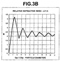
- FIGS. 3A, 3B and 3C states of the oscillations of M when the relative refractive index n is 1.1, 1.5 and 2.1 are shown in FIGS. 3A, 3B and 3C, respectively. From these graphs, it is understood that the scattering cross section ⁇ in the Mie scattering region comes to oscillate/converge owing to an increase of the particle diameter Dn. In this oscillation region also, it is possible to obtain, in a wide range where the relative refractive index n is approximately 1 to 2, a numeric value to be multiplied to the geometric scattering cross section ⁇ a P 2 in which the Mie scattering region converges, in response to the respective particle diameters from FIGS. 3A to 3C.
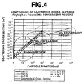
- results of obtaining a relationship between the particle diameter Dp and the scattering cross section ⁇ based on the above-described expressions (7) and (9) for each of some refractive indices n are shown in FIG. 4. Meanwhile, results of obtaining a relationship between the particle diameter Dp of the multi-particle system and an inverse number of a particle density to which a certain numeric value is multiplied, based on the Mie scattering theory by means of computer simulation, are shown in FIG. 5.
- K C is a dimension less correction coefficient empirically obtained when the light propagates through the optical medium of the limited space.
- parameters generally required in designing the light guide are the volume V of the optical medium, the number of mixed particles N PT and the particle diameter Dp, and how the intensity of the emitted light is changed in this case is examined.
- the taking-out efficiency Eout can be determined by the scattering cross section ⁇ of the particles, the particle density Np, the length L G of the optical medium in the light propagation direction, the correction coefficient K C and the loss coefficient K L .
- the light taking-out efficiency Eout is realized if the above-described expression (14) is satisfied.
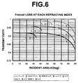
- the Fresnel loss on the boundary surfaces is represented as:
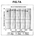
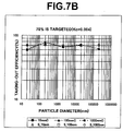
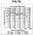
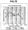
- FIGS. 7A to 7E show, for light taking-out efficiencies as average targets of the respective particle diameters, which are first determined, calculated values (10 mmC, 100 mmC and 1000 mmC) in the respective particle diameters and results of a precise simulation (S 10 mm, S 100 mm and S 1000 mm) by the particle diameters and the densities for use in this calculation method.
- the light taking-out efficiencies as the average targets are 80%, 70%, 60%, 50% and 40% in FIGS. 7A, 7B, 7C, 7D and 7E, respectively.
- the scattering cross section ⁇ is obtained according to the Rayleigh theory when the particle diameter is 20 nm, and according to the Mie theory when the particle diameter is 200 nm or more.
- Reference symbol S denotes the results of the simulation, and reference symbol C denotes the results of this calculation.
- numeric values represent the lengths L G of the optical medium in the light propagation direction.
- FIGS. 7A to 7E it is understood that, when the light taking-out efficiencies as the average targets are 60% or more, errors from the results of the simulation remain within a range of less than 10%, and that both coincide well with each other. Specifically, in other words, FIGS. 7A to 7E show that the errors remain within the range of less than 10% when the value of ⁇ •Np•L G •K C is 0.4 or less. Moreover, FIGS. 7A to 7E simultaneously show that the errors remain within a range of less than 50% even if the above-described value is 0.9 or less. Note that 0.92, which is an empirically obtained value, is used as the value of K L .
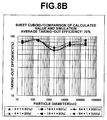
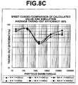
- Tables 1 to 3 and FIGS. 8A to 8C Results of performing the calculation for the sheet cuboid based on expression (14) are shown in Tables 1 to 3 and FIGS. 8A to 8C. Note that it is FIG. 8A that shows numeric values of Table 1 in a graph, and in a similar manner, Table 2 and Table 3 correspond to FIG. 8B and FIG. 8C, respectively. In the calculation results in these Tables, any of the values of ⁇ •Np•L G •K C is 0.9 or less. Note that, in all of the cases, a value of K L is 0.92.
- Eout 0.8 Particle diameter (nm) Scattering cross section (m 2 ) Particle density (pieces/mm 3 ) W ⁇ T ⁇ L G (mm) Taking-out efficiency, expression (14) (%) Taking-out efficiency, SIM (%) 20 1.1 ⁇ 10 -22 1.0 ⁇ 10 13 4 ⁇ 1 ⁇ 20 84 87 2.5 ⁇ 10 12 16 ⁇ 1 ⁇ 80 88 6.3 ⁇ 10 11 64 ⁇ 1 ⁇ 320 88 200 1.5 ⁇ 10 -14 3.0 ⁇ 10 7 4 ⁇ 1 ⁇ 20 89 89 7.5 ⁇ 10 6 16 ⁇ 1 ⁇ 80 89 1.9 ⁇ 10 8 64 ⁇ 1 ⁇ 320 89 2000 12.6 ⁇ 10 -12 3.0 ⁇ 10 5 4 ⁇ 1 ⁇ 20 68 75 7.5 ⁇ 10 4 16 ⁇ 1 ⁇ 80 76 1.9 ⁇ 10 4 64 ⁇ 1 ⁇ 320 76 20000 6.3 ⁇ 10 -10 3.0 ⁇ 10 3 4 ⁇ 1 ⁇ 20 79 86 7.5 ⁇ 10 2 16 ⁇ 1 ⁇ 80 86 1.9 ⁇ 10 2 64 ⁇ 1 ⁇ 320 86 200000 6.3 ⁇ 10 -8 3.0 ⁇ 10 1 4 ⁇ 1
- FIGS. 8A and 8C lines denoted by reference symbols (C) and (S) represent the results of this calculation and the precise simulation, respectively. Moreover, numeric values represent dimensions (mm) of the optical mediums. Furthermore, the light taking-out efficiencies as the targets are set at the averages in the respective particle diameters. As apparent from Tables 1 to 3 and FIGS. 8A to 8C, it is understood that the results of this calculation and the results of the simulation coincide well with each other. In particular, the results for the case in which the particle diameter is 2000 nm make it far more apparent that this calculation method coincides with the simulation.
- Distribution characteristics of emitted light intensity are affected by an intensity distribution of light from light sources, an angle of divergence thereof, the number and location of the light sources and the like, and were accordingly evaluated by the simulation.
- the distribution characteristics of the emitted light intensity for each particle diameter, which were thus obtained, are shown in FIGS. 9A, 9B and 9C.
- the light source is located at a center of an incident-side cross section of the optical medium, and the angle of divergence is set at 30° by a half angle.
- FIGS. 9A, 9B and 9C show results of performing the simulation for the case of the sheet cuboids under the same conditions as in Table 1, and show the results of the cases where sheet sizes thereof are small, medium and large, respectively.
- the sheet light guide for use in the present invention is configured to satisfy the relationship of: ⁇ •Np•L G •K C ⁇ 0 as described above, then the errors from the results of the simulation remain within the range of less than 10%. Therefore, good light taking-out efficiency and an even intensity distribution of the emitted light can be realized.
- the sheet light guide for use in the present invention is that which propagates light therethrough while making the light repeatedly scatter by the particles in the optical medium. Accordingly, both of the following are possible in a similar way: one is to make the light incident from one end surface and to propagate the light to the other end surface; and the other is to make the light incident from the above-described other end surface and to propagate the light to the above-described one end surface. Accordingly, it becomes possible for a communication system using the sheet light guide of the present invention to perform two-way communication.
- a sheet light guide 10 is that which is formed by containing the light-scattering particles in the optical medium such as, for example, polymethylmethacrylate (PMMA), and propagates light incident from one end surface to the other end surface side while scattering the light by the particles.
- the optical medium such as, for example, polymethylmethacrylate (PMMA)
- a plurality of optical fibers 21, 22 and 23 are connected to the one end surface of the sheet light guide 10
- optical fibers 31, 32 and 33 are connected to the other end surface.
- N.A. ones with large numerical apertures
- the photodetector is a PIN photodiode, and accordingly, this condition is not helpful in the case where the photodetector is different (for example, photomultiplier, avalanche photodiode and the like) , or in the case where a transmission band is different.
- the minimum received optical power which is acceptable in a certain transmission band should be present.
- the acceptable minimum received optical power of the photodetector which satisfies the above-described condition, is defined as P(Receiver)min.
- constraints in the case where the intensity distribution of the emitted light of the sheet light guide is flat are obtained from the above-described condition. Even if the intensity distribution of the emitted light is flat, in one optical fiber, an area ratio n/4 of the light guide path and the optical fiber in cross section necessarily lead to a loss. However, it is assumed that a core diameter of the optical fiber is equal to the thickness of the sheet light guide. Moreover, a tolerance is not considered at present.
- FIG. 11 A relationship between the received optical power and the number of branches (number of nodes) is shown in FIG. 11 for the cases where the incident optical power is 1 mW and 10 mW.
- the received optical power is proportional to the optical power of emitted light.
- the intensity distribution of the light emitted from the sheet light guide is a flat one, actually, when the position of the light source is changed, the intensity distribution of the emitted light is also changed.
- fluctuations occur in the received optical power, and that the received optical power becomes the minimum at a portion where the intensity of incident light is the minimum.
- a distribution profile of the emitted light when the light source is at an arbitrary position is represented by a normalization intensity distribution function D(x, y), in which a direction where the intensity distribution of the emitted light is on a long side is taken as x, and a direction where the intensity distribution thereof is on a short side is taken as y.
- D(x, y) a normalization intensity distribution function
- Segmax denotes a segment in which the optical power becomes the maximum among all the segments.
- NPi is represented as:
- P(Receiver_min) dBm -10 Log ⁇ Pin • Eout •( NPi (min)/ ⁇ NPi )• ⁇ /4 ⁇
- PRmin dBm PR min dBm ⁇ P (Re
- PRmin dBm is represented as: PR min dBm ⁇ P (Re DC _min) dBm • K E • K F • K R • K FI This expression (29) becomes the necessary condition for the communication system using the sheet light guide.
- the BER is an index indicating how much difference occurs between an original digital signal randomly generated and a received digital signal as a result of transmitting the digital signal through a certain communication medium.
- bit error generation a mechanism of the bit error generation is considered.
- a distortion of an analog waveform when an analog signal is converted into a digital signal is mentioned as a first factor.
- the bit error is increased when a signal level is lowered, and accordingly, it is also necessary to consider S/N as a factor. Even if the signal level is lowered owing to the distortion of the waveform, the bit error should not occur when the signal level stably exceeds a threshold value for distinguishing (0, 1) signals.
- a threshold value for distinguishing (0, 1) signals.
- the maximum factor of the waveform distortion in the communication system using the sheet light guide is conceived to be a distortion of a received signal itself in which an arbitrary incident segment and an emitted segment correspond to each other, and a waveform distortion owing to a phase shift of each signal component included in a mixing signal corresponding to each incident segment and an arbitrary emitted segment.
- the above-described waveform distortion results from an optical path difference of signal light.
- Elements causing the optical path difference in the communication system using the optical fibers and the sheet light guide are the sheet light guide itself and the optical fibers.
- the bit error is estimated to occur because the signal level is lowered than a predetermined threshold value by the waveform distortion when the analog signal is converted into the digital signal.
- the bit error occurs when the phase difference (jitter) is increased between the reference signal and the digitized signal.
- an analog signal in the vicinity of the threshold value fluctuates with respect to the threshold value owing to fluctuations by the noise, and is converted into an erroneous digital signal.
- the bit error is conceived to occur because the factor of the optical path difference and the factor of the noise are combined.
- an outer diameter of each optical fiber is 1 mm, and a length thereof is 1 m, in which case the optical path difference is negligible.
- the optical fibers are provided in parallel while being brought into intimate contact with one another on both the light incident side and the light emitting side.
- numeric values of "In” and “Out” in each graph represent a light incident position and a light emitting position by distances from a center position of the sheet light guide in the direction where the optical fibers are arrayed.
- the distances are represented by mm, and positions on a side where the optical fibers onto which the light is made incident are present are denoted by negative symbols (-), and positions on the other side are denoted by positive symbols (+).
- FIG. 13A shows a waveform distortion in the case where the light is made incident onto an optical fiber having a center at a position of -1.5 mm from the above-described center position, that is, the second optical fiber from the center position in the negative direction and the light is emitted from an optical fiber having a center at the same position.
- FIG. 13B shows a waveform distortion in the case where the light is made incident onto the optical fiber at the same position and the light is emitted from an optical fiber having a center at a position of +1.5 mm from the above-described center position, that is, a second optical fiber from the center position in the positive direction.
- FIG. 13B shows a waveform distortion in the case where the light is made incident onto the optical fiber at the same position and the light is emitted from an optical fiber having a center at a position of +1.5 mm from the above-described center position, that is, a second optical fiber from the center position in the positive direction.
- FIG. 13B shows a waveform distortion in the case
- FIG. 14A shows a waveform distortion in the case where the light is made incident onto an optical fiber having a center at a position of -3.5 mm from the above-described center position, that is, a fourth optical fiber from the center position in the negative direction and the light is emitted from an optical fiber having a center at the same position.
- FIG. 14B shows a waveform in the case where the light is made incident onto the optical fiber having the center at the same position and the light is emitted from an optical fiber having a center at a position of +3.5 mm from the center position, that is, a fourth optical fiber from the center position in the positive direction. Furthermore, FIG.
- FIG. 15A shows a waveform distortion in the case where the light is made incident onto an optical fiber having a center at a position of -7.5 mm from the above-described center position, that is, an eighth optical fiber from the center position in the negative direction and the light is emitted from an optical fiber having a center at the same position.
- FIG. 15B shows a waveform in the case where the light is made incident onto the optical fiber at the same position as described above and the light is emitted from an optical fiber having a center at a position of +7.5 mm from the above-described center position, that is, an eighth optical fiber from the center position in the positive direction.
- bit error an occurrence of erroneous reading (bit error) is also associated with quality of the signal, that is, S/N. Specifically, even if main components from which harmonic components are removed are separated in signal spectra adjacent to one another, if the harmonic components (noise components) are large, signals cannot be distinguished as individual signals. Supposing an extreme case, it is conceived that it is usually impossible to detect such a signal embedded in the noise components unless the signal is particularly subjected to filtering processing.
- noise component there is extraneous noise such as radiation noise and induction noise, in addition to noise occurring in the inside of the system, such as thermal noise (Johnson Noise), quantum noise (Shot Noise), 1/f noise intrinsic to a semiconductor device for use in the light emitter and the photodetector.
- thermal noise Johnson Noise
- Shot Noise quantum noise
- 1/f noise intrinsic to a semiconductor device for use in the light emitter and the photodetector.
- Noise(Total) Noise (heat)+Noise (quantum)
- Noise ( heat ) (4 kT / R )• ⁇
- the band of the photodiode is 0.25 GHz.
- S/Naccept When expression (35) reaches a certain value, the BE occurs at a certain probability, which is defined as S/Naccept.
- the probability of occurrence of the Noise(System_rms) is equal to the BER.
- FIG. 17 shows a relationship between the BER calculated based on the above-described consideration and the received optical power.
- the BE occurs when a value obtained by subtracting the noise component from the signal component is lowered than the V (Thresh) or when a value obtained by adding the noise component to the "0" level exceeds the V(Thresh). Therefore, it is desirable that the V(Thresh) be set at a half value of an average signal voltage.
- a communication system configured in the following manner can be defined.
- the acceptable BER that is, BER(accept)
- the rms noise of the system is defined as the Noise(System_rms)
- the probability of occurrence Pr(Noise(System_rms)) of the Noise (System_rms) is Noise (Systme_rms) of amagnitude which satisfies the following in a band where it is not necessary to consider the distortion of the signal waveform: Pr( Noise ( System_rms )• Q ) ⁇ BER ( accept ) where Q is a proportionality constant.
- the signal level is of the input signal PRmin which satisfies: ⁇ S ( PR min) v - V ( Thresh ) ⁇ > Noise ( System_rms )• Q Moreover, the signal level is of the signal voltage S(PRmin)v outputted through a load resistor from a photodetector which satisfies expression (37).
- the above-described expression (37) can also be defined as: S ( PR min) v /2 > Noise ( System_rms )• Q
- the output power PRmin of the light source is adjusted so as to satisfy the BER(accept), and thus expression (37) and expression (38) may be satisfied.
- a digital circuit which makes feedback from the BER measurement circuit to the light source side is provided, and this digital circuit is made as one which controls the optical power of the light source according to a table determined based on the BER (accept).
- the digital circuit becomes capable of also coping with the extraneous noise other than the Noise(System_rms) generated by the system itself.
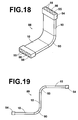
- FIG. 18 shows a perspective shape of a communication system using a sheet light guide according to an embodiment of the present invention.
- this system is configured by use of a light guide 88 having a bent portion.
- This light guide 88 is composed of two sheet light guides 10, each of which has basically the same configuration as that previously shown in FIG. 10, and of an angle-converting light guide 90 to which each of these sheet light guides 10 is optically coupled.
- the angle-converting light guide 90 has a cross-sectional shape of a quartered circular ring, and is in a state where an end surface thereof coupled to one of the sheet light guides 10 and an end surface coupled to the other sheet light guide 10 make an angle of 90°.
- This angle-converting light guide 90 is formed by performing injection molding of resin such as, for example, polymethylmethacrylate (PMMA), and maintains the above-described shape as long as no large external force is applied thereto in particular.
- PMMA polymethylmethacrylate
- the sheet light guide 10 is formed by containing light-scattering particles in an optical medium such as, for example, the PMMA, and propagates light incident from one end surface to the other end surface side while scattering the light by the particles. Then, a light transmitting/receiving unit 54 is attached onto an end surface of each sheet light guide 10, which is on an opposite side to the angle-converting light guide 90.
- Each light transmitting/receiving unit 54 of this embodiment is composed of three photodetectors 55 and one phototransmitter 56.
- Signal light emitted from the phototransmitter 56 of the light transmitting/receiving unit 54 coupled to the one of the sheet light guides 10 propagates through this sheet light guide 10 in the above-described manner, changes a propagation direction thereof by 90° in the angle-converting light guide 90, and is made incident onto the other sheet light guide 10. Then, the signal light propagates through the other sheet light guide 10 in a similar way, and is received by the three photodetectors 55 of the light transmitting/receiving unit 54 coupled thereto.
- the sheet light guide In the case of introducing a communication system using a sheet light guide into various instruments, the sheet light guide must be often bent. However, in general, the sheet light guide has some thickness and is not very flexible. Accordingly, when a space in such an instrument is narrow, it becomes sometimes impossible to place the sheet light guide therein in a bent manner. This point becomes a serious problem in terms of replacing a communication system using electric wires in the instrument by the communication system using the sheet light guide.
- the communication system of this embodiment includes the angle-converting light guide 90 as described above.
- the communication system of this embodiment becomes widely applicable one in place of the communication system using, for example, a flexible board and a flat cable which have been heretofore used for wiring in the narrow instrument.
- this communication system is not only capable of replacing the above-described conventional system but also resistant to electromagnetic noise because the communication system performs communication by means of optical signals.
- the communication system becomes one constructible at low cost as compared with a communication system using optical fibers among communication systems performing communications by means of the optical signals.
- the angle-converting light guide 90 may be formed of a material different from the material of the sheet light guides 10 without being limited thereto. Moreover, the angle-converting light guide 90 is formed separately from the sheet light guides 10, and then coupled to the sheet light guides 10. However, from the beginning, the angle-converting light guide 90 may be formed integrally with the sheet light guides 10 by the injection molding and the like. Furthermore, the light-scattering particles may be or may not be contained in this angle-converting light guide 90 as in the sheet light guides 10. However, it is naturally desirable that the light-scattering particles be contained in the angle-converting light guide 90 in terms of making an intensity distribution of emitted light even.
- a shape of the angle-converting light guide is not limited to one like that of the angle-converting light guide 90 described above, and shapes as illustrated in FIGS. 20A to 20C can be adopted as appropriate.
- FIGS. 20A to 20C show cross-sectional shapes in planes orthogonal to a width direction of the angle-converting light guide.
- An angle-converting light guide 90a shown in FIG. 20A is that which converts the light propagation angle by 90° as in the above-described angle-converting light guide 90, but has a cross-sectional shape not of a circular arc but of bent straight lines.
- an angle-converting light guide 90b shown in FIG. 20B is that which converts the light propagation angle by 180° and has a circular arc cross-sectional shape.
- an angle-converting light guide 90c shown in FIG. 20C is that which converts the light propagation angle by 180° as in the above-described angle-converting light guide 90b, but has a cross-sectional shape not of a circular arc but of bent straight lines.
Landscapes
- Physics & Mathematics (AREA)
- General Physics & Mathematics (AREA)
- Optics & Photonics (AREA)
- Engineering & Computer Science (AREA)
- Microelectronics & Electronic Packaging (AREA)
- Optical Couplings Of Light Guides (AREA)
- Optical Elements Other Than Lenses (AREA)
Applications Claiming Priority (2)
| Application Number | Priority Date | Filing Date | Title |
|---|---|---|---|
| JP2004019970A JP2005215169A (ja) | 2004-01-28 | 2004-01-28 | シート状導光体を用いた通信システム |
| JP2004019970 | 2004-01-28 |
Publications (1)
| Publication Number | Publication Date |
|---|---|
| EP1560049A1 true EP1560049A1 (de) | 2005-08-03 |
Family
ID=34650788
Family Applications (1)
| Application Number | Title | Priority Date | Filing Date |
|---|---|---|---|
| EP05001678A Withdrawn EP1560049A1 (de) | 2004-01-28 | 2005-01-27 | Kommunikationsystem mit flächigem Lichtwellenleiter |
Country Status (3)
| Country | Link |
|---|---|
| US (1) | US7190857B2 (de) |
| EP (1) | EP1560049A1 (de) |
| JP (1) | JP2005215169A (de) |
Families Citing this family (4)
| Publication number | Priority date | Publication date | Assignee | Title |
|---|---|---|---|---|
| CN1517734A (zh) * | 2003-01-28 | 2004-08-04 | ��ʿ��Ƭ��ʽ���� | 使用片状导光体的通信系统 |
| US8251562B2 (en) * | 2006-07-21 | 2012-08-28 | Fujifilm Corporation | Unitary light guide plate, light guide plate unit, planar lighting device and liquid crystal display device |
| JP5142500B2 (ja) * | 2006-08-24 | 2013-02-13 | 株式会社フジクラ | 光路変換光コネクタ |
| US9585548B2 (en) * | 2013-03-12 | 2017-03-07 | Schott Corporation | Optical element for Mie scattering light from an optical fiber |
Citations (1)
| Publication number | Priority date | Publication date | Assignee | Title |
|---|---|---|---|---|
| EP1443348A2 (de) * | 2003-01-28 | 2004-08-04 | Fuji Photo Film Co., Ltd. | Flächiger Lichtwellenleiter und bidirektionales Kommunikationsystem mit flächigem Lichtwellenleiter |
Family Cites Families (7)
| Publication number | Priority date | Publication date | Assignee | Title |
|---|---|---|---|---|
| WO1993006509A1 (en) * | 1991-09-27 | 1993-04-01 | Yasuhiro Koike | Light-scattering light guide and its manufacture, and applied optics apparatus thereof |
| US5548670A (en) * | 1992-11-27 | 1996-08-20 | Koike; Yasuhiro | Light-scattering light-guiding device |
| US5822475A (en) * | 1995-12-20 | 1998-10-13 | Fuji Xerox Co., Ltd. | Optical bus and signal processor |
| JP3666190B2 (ja) | 1997-07-14 | 2005-06-29 | 富士ゼロックス株式会社 | 光バスおよび信号処理装置 |
| JPH11326644A (ja) * | 1998-05-20 | 1999-11-26 | Bridgestone Corp | 光伝送チューブ及びその製造方法 |
| US6205263B1 (en) * | 1999-06-16 | 2001-03-20 | Intelligent Optical Systems | Distributed optical fiber sensor with controlled response |
| JP2004226584A (ja) * | 2003-01-22 | 2004-08-12 | Fuji Xerox Co Ltd | 光信号伝送装置、及び信号処理装置 |
-
2004
- 2004-01-28 JP JP2004019970A patent/JP2005215169A/ja active Pending
-
2005
- 2005-01-27 EP EP05001678A patent/EP1560049A1/de not_active Withdrawn
- 2005-01-28 US US11/044,061 patent/US7190857B2/en not_active Expired - Fee Related
Patent Citations (1)
| Publication number | Priority date | Publication date | Assignee | Title |
|---|---|---|---|---|
| EP1443348A2 (de) * | 2003-01-28 | 2004-08-04 | Fuji Photo Film Co., Ltd. | Flächiger Lichtwellenleiter und bidirektionales Kommunikationsystem mit flächigem Lichtwellenleiter |
Also Published As
| Publication number | Publication date |
|---|---|
| JP2005215169A (ja) | 2005-08-11 |
| US20050163422A1 (en) | 2005-07-28 |
| US7190857B2 (en) | 2007-03-13 |
Similar Documents
| Publication | Publication Date | Title |
|---|---|---|
| US9791347B2 (en) | Method and system for non-contact optical-power measurement | |
| KR100984763B1 (ko) | 시트형상 도광체의 설계 방법 및 이를 사용한 통신 시스템 | |
| US7526156B2 (en) | Optical fiber for out-coupling optical signal and apparatus for detecting optical signal using the same optical fiber | |
| EP1561133A1 (de) | Optische linsen | |
| TW200411215A (en) | Symmetric, bi-aspheric lens for use in transmissive and reflective optical fiber components | |
| JPWO2005124415A1 (ja) | 一方向性光パワーモニター | |
| JP6477201B2 (ja) | 光モジュール | |
| JP4153441B2 (ja) | シート状導光体およびそれを用いた通信システム | |
| EP1560049A1 (de) | Kommunikationsystem mit flächigem Lichtwellenleiter | |
| Bian et al. | High-power, low-loss, fabrication tolerant multi-tip SiN edge coupler in 300mm monolithic SiPh foundry technology | |
| EP1560051A1 (de) | Kommunikationsystem mit flächigem Lichtwellenleiter | |
| US6793411B2 (en) | Method and apparatus for communicating signals with an optical fiber | |
| EP1560050A1 (de) | Flächiger Lichtwellenleiter und Kommunikationsystem welches diesen nutzt | |
| JP4475562B2 (ja) | シート状導光体の設計方法 | |
| US7224877B2 (en) | Communication system using sheet light guide | |
| Wells | Crosstalk in a bidirectional optical fiber | |
| Hirano et al. | Extremely Low-Profile Single Mode Fiber Array Coupler Suitable for Silicon Photonics | |
| Steinegger et al. | Design and analysis of coupling elements between optical fibres and optical free space | |
| CN201434921Y (zh) | 具有降低vcsel频谱宽度的光纤接头 | |
| Hsu et al. | Characterization and analysis of graded index optical waveguides for the realization of low-power, high-density, and high-speed optical link | |
| Ientilucci | Fundamentals of Fiber Optics | |
| Lorenz et al. | Multimode Bus Coupler for Device Communication Integrated in 3D-Opto-MID | |
| Hong et al. | Optical interconnection testbed using fiber image guides | |
| Takeyoshi et al. | Densely aligned multichannel polymer waveguide with low inter-channel crosstalk | |
| Buchanan | Fiber Optic Systems |
Legal Events
| Date | Code | Title | Description |
|---|---|---|---|
| PUAI | Public reference made under article 153(3) epc to a published international application that has entered the european phase |
Free format text: ORIGINAL CODE: 0009012 |
|
| AK | Designated contracting states |
Kind code of ref document: A1 Designated state(s): AT BE BG CH CY CZ DE DK EE ES FI FR GB GR HU IE IS IT LI LT LU MC NL PL PT RO SE SI SK TR |
|
| AX | Request for extension of the european patent |
Extension state: AL BA HR LV MK YU |
|
| 17P | Request for examination filed |
Effective date: 20051229 |
|
| AKX | Designation fees paid |
Designated state(s): DE FR GB NL |
|
| STAA | Information on the status of an ep patent application or granted ep patent |
Free format text: STATUS: THE APPLICATION IS DEEMED TO BE WITHDRAWN |
|
| 18D | Application deemed to be withdrawn |
Effective date: 20060808 |