EP1558952B1 - Optischer 2 x n leistungsteiler in integrierter optik - Google Patents
Optischer 2 x n leistungsteiler in integrierter optik Download PDFInfo
- Publication number
- EP1558952B1 EP1558952B1 EP03780301A EP03780301A EP1558952B1 EP 1558952 B1 EP1558952 B1 EP 1558952B1 EP 03780301 A EP03780301 A EP 03780301A EP 03780301 A EP03780301 A EP 03780301A EP 1558952 B1 EP1558952 B1 EP 1558952B1
- Authority
- EP
- European Patent Office
- Prior art keywords
- guides
- divider
- coupling
- guide
- wavelengths
- Prior art date
- Legal status (The legal status is an assumption and is not a legal conclusion. Google has not performed a legal analysis and makes no representation as to the accuracy of the status listed.)
- Expired - Lifetime
Links
- 230000003287 optical effect Effects 0.000 title claims abstract description 24
- 230000008878 coupling Effects 0.000 claims abstract description 77
- 238000010168 coupling process Methods 0.000 claims abstract description 77
- 238000005859 coupling reaction Methods 0.000 claims abstract description 77
- 230000003595 spectral effect Effects 0.000 claims description 24
- 239000000758 substrate Substances 0.000 claims description 21
- 238000005342 ion exchange Methods 0.000 claims description 5
- 239000011521 glass Substances 0.000 claims description 4
- 238000000926 separation method Methods 0.000 abstract 3
- 238000000034 method Methods 0.000 description 8
- 238000013459 approach Methods 0.000 description 6
- 229920000297 Rayon Polymers 0.000 description 2
- 230000007423 decrease Effects 0.000 description 2
- 238000005516 engineering process Methods 0.000 description 2
- 235000021183 entrée Nutrition 0.000 description 2
- 230000003993 interaction Effects 0.000 description 2
- 239000002964 rayon Substances 0.000 description 2
- 239000002356 single layer Substances 0.000 description 2
- 230000008859 change Effects 0.000 description 1
- 230000003247 decreasing effect Effects 0.000 description 1
- 230000001419 dependent effect Effects 0.000 description 1
- 230000008021 deposition Effects 0.000 description 1
- 238000010586 diagram Methods 0.000 description 1
- 238000005530 etching Methods 0.000 description 1
- 230000000873 masking effect Effects 0.000 description 1
- 239000011159 matrix material Substances 0.000 description 1
- 230000000644 propagated effect Effects 0.000 description 1
- 230000001902 propagating effect Effects 0.000 description 1
- 230000004044 response Effects 0.000 description 1
- 230000001629 suppression Effects 0.000 description 1
Images


Classifications
-
- G—PHYSICS
- G02—OPTICS
- G02B—OPTICAL ELEMENTS, SYSTEMS OR APPARATUS
- G02B6/00—Light guides; Structural details of arrangements comprising light guides and other optical elements, e.g. couplings
- G02B6/24—Coupling light guides
- G02B6/26—Optical coupling means
- G02B6/28—Optical coupling means having data bus means, i.e. plural waveguides interconnected and providing an inherently bidirectional system by mixing and splitting signals
- G02B6/2804—Optical coupling means having data bus means, i.e. plural waveguides interconnected and providing an inherently bidirectional system by mixing and splitting signals forming multipart couplers without wavelength selective elements, e.g. "T" couplers, star couplers
- G02B6/2821—Optical coupling means having data bus means, i.e. plural waveguides interconnected and providing an inherently bidirectional system by mixing and splitting signals forming multipart couplers without wavelength selective elements, e.g. "T" couplers, star couplers using lateral coupling between contiguous fibres to split or combine optical signals
-
- G—PHYSICS
- G02—OPTICS
- G02B—OPTICAL ELEMENTS, SYSTEMS OR APPARATUS
- G02B6/00—Light guides; Structural details of arrangements comprising light guides and other optical elements, e.g. couplings
- G02B6/10—Light guides; Structural details of arrangements comprising light guides and other optical elements, e.g. couplings of the optical waveguide type
- G02B6/12—Light guides; Structural details of arrangements comprising light guides and other optical elements, e.g. couplings of the optical waveguide type of the integrated circuit kind
- G02B6/122—Basic optical elements, e.g. light-guiding paths
- G02B6/125—Bends, branchings or intersections
-
- G—PHYSICS
- G02—OPTICS
- G02B—OPTICAL ELEMENTS, SYSTEMS OR APPARATUS
- G02B6/00—Light guides; Structural details of arrangements comprising light guides and other optical elements, e.g. couplings
- G02B6/10—Light guides; Structural details of arrangements comprising light guides and other optical elements, e.g. couplings of the optical waveguide type
- G02B6/12—Light guides; Structural details of arrangements comprising light guides and other optical elements, e.g. couplings of the optical waveguide type of the integrated circuit kind
- G02B6/13—Integrated optical circuits characterised by the manufacturing method
- G02B6/134—Integrated optical circuits characterised by the manufacturing method by substitution by dopant atoms
- G02B6/1345—Integrated optical circuits characterised by the manufacturing method by substitution by dopant atoms using ion exchange
-
- G—PHYSICS
- G02—OPTICS
- G02B—OPTICAL ELEMENTS, SYSTEMS OR APPARATUS
- G02B6/00—Light guides; Structural details of arrangements comprising light guides and other optical elements, e.g. couplings
- G02B6/10—Light guides; Structural details of arrangements comprising light guides and other optical elements, e.g. couplings of the optical waveguide type
- G02B6/12—Light guides; Structural details of arrangements comprising light guides and other optical elements, e.g. couplings of the optical waveguide type of the integrated circuit kind
- G02B2006/12083—Constructional arrangements
- G02B2006/121—Channel; buried or the like
-
- G—PHYSICS
- G02—OPTICS
- G02B—OPTICAL ELEMENTS, SYSTEMS OR APPARATUS
- G02B6/00—Light guides; Structural details of arrangements comprising light guides and other optical elements, e.g. couplings
- G02B6/10—Light guides; Structural details of arrangements comprising light guides and other optical elements, e.g. couplings of the optical waveguide type
- G02B6/12—Light guides; Structural details of arrangements comprising light guides and other optical elements, e.g. couplings of the optical waveguide type of the integrated circuit kind
- G02B2006/12133—Functions
- G02B2006/12147—Coupler
-
- G—PHYSICS
- G02—OPTICS
- G02B—OPTICAL ELEMENTS, SYSTEMS OR APPARATUS
- G02B6/00—Light guides; Structural details of arrangements comprising light guides and other optical elements, e.g. couplings
- G02B6/10—Light guides; Structural details of arrangements comprising light guides and other optical elements, e.g. couplings of the optical waveguide type
- G02B6/12—Light guides; Structural details of arrangements comprising light guides and other optical elements, e.g. couplings of the optical waveguide type of the integrated circuit kind
- G02B2006/12133—Functions
- G02B2006/1215—Splitter
-
- G—PHYSICS
- G02—OPTICS
- G02B—OPTICAL ELEMENTS, SYSTEMS OR APPARATUS
- G02B6/00—Light guides; Structural details of arrangements comprising light guides and other optical elements, e.g. couplings
- G02B6/24—Coupling light guides
- G02B6/26—Optical coupling means
- G02B6/28—Optical coupling means having data bus means, i.e. plural waveguides interconnected and providing an inherently bidirectional system by mixing and splitting signals
- G02B6/293—Optical coupling means having data bus means, i.e. plural waveguides interconnected and providing an inherently bidirectional system by mixing and splitting signals with wavelength selective means
- G02B6/29346—Optical coupling means having data bus means, i.e. plural waveguides interconnected and providing an inherently bidirectional system by mixing and splitting signals with wavelength selective means operating by wave or beam interference
- G02B6/2935—Mach-Zehnder configuration, i.e. comprising separate splitting and combining means
- G02B6/29352—Mach-Zehnder configuration, i.e. comprising separate splitting and combining means in a light guide
Definitions
- the present invention relates to an optical divider 2 to n in integrated optics. More specifically, it relates to an optical splitter having satisfactory excess losses and achromatism for the targeted applications and in particular for applications in the field of optical telecommunications, in particular in the spectral windows 1260-1360 nm and 1480-1660 nm.
- the invention applies to all domains requiring an optical function 2 to n and more particularly to the telecommunications field.
- An optical divider 2 to n (with n integer greater than or equal to 2) is composed of at least one optical divider element having 2 inputs and 2 outputs for dividing a light wave injected into one of the two-part inputs, distributed according to a predefined division ratio in each of the outputs.
- the optical divider comprises several divider elements cascaded so as to have 2 inputs and n outputs and allow the distribution of a light wave injected into one of the 2 inputs on the n outputs in a predefined division ratio for each of the outputs.
- a conventional divider 2 to 2 is for example described in US Patent 5,835,651.
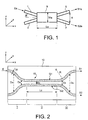
- FIG. 1 schematically represents a conventional 2-to-2 divider of this type realized in integrated optics, in a xy plane of the substrate containing said divider.
- first and second monomode input waveguides 1 and 3 are shown, a first and a second monomode output waveguide 5 and 7 and a bi-mode waveguide 9 of length La x-axis and width Wa along the y-axis, connecting the input waveguides and the output waveguides.
- the input and output guides are respectively connected to the dual-mode guide, with an angle ⁇ with respect to the x-axis.
- a light wave Ea injected into one of the input single-mode guides, for example the guide 1 is propagated therein in the direction of the bi-mode guide 9 while approaching the second input guide 3 thus establishing with the latter a proximity coupling.
- This proximity coupling is more important for high wavelengths (such as wavelengths in the 1480-1660 nm spectral band) than for low wavelengths (such as wavelengths in the 1260-1360 nm spectral band).
- the light wave couples to the two modes of the dual-mode guide 9.
- the coupling between these two modes during the propagation in the dual-mode guide has a spectral behavior contrary to that experienced in monomode guides, ie a lower coupling for long wavelengths (1480-1660 nm) than for low wavelengths (1260-1360 nm).
- the light wave couples with a certain distribution on the two monomode output guides 5, 7.
- the light wave then undergoes again proximity coupling and this until that the monomode guides are separated by a distance H such that the light wave propagating in each of the single-mode guides no longer sees the other guide.
- the spectral behavior in the single-mode input and output guides which is contrary to the spectral behavior in the two-mode guide, allows for well-chosen values of ⁇ , Wa and La to obtain a 2-to-2 achromatic divider. .
- a low value of ⁇ also makes it possible to limit excess losses.
- the light wave undergoes a discontinuity at each end of the dual-mode guide connected to the monomode guides creating mismatch losses between modes of the two-mode guide and modes of the single-mode guides, as well as reflection losses. These losses of mismatch and reflection are particularly troublesome for applications in the field of optical telecommunications.
- the present invention relates to an optical divider 2 to n in integrated optics not having the limitations and difficulties of the dividers of the prior art.
- an object of the invention is to provide a divider 2 to n having low excess losses and satisfactory achromatism especially for optical telecommunications in all spectral windows 1260-1360 nm and 1480-1660 nm.
- the divider of the invention is advantageously very slightly chromatic or even achromatic and has a minimum of excess losses.
- achromatic is understood to mean both low chromaticity (by example ⁇ 0.5 dB for the spectral windows of telecommunications) that a "perfect" achromatism.
- An object of the invention is also to provide a divider 2 to n in which excess losses and chromaticism are independent to facilitate its implementation.
- An object of the invention is also to provide a divider 2 to n not having a discontinuity for the light wave to limit losses of mismatch and reflection.
- This divider operates according to the characteristics stated in the characterizing part of claim 1.
- the light wave is divided according to a division ratio CR which is related to the output of one of the first or second guides (by convention).
- optical guide in the invention means a lateral confinement guide, as opposed to a planar guide in which the light can propagate in a plane: the plane of the guide.
- the guides of the invention are favorably monomode.
- An optical guide consists of a central part generally called heart and surrounding environments located all around the heart and which may be identical to each other or different.
- the refractive index of the medium composing the heart must be different and in most cases higher than those of the surrounding environment.
- the guide to its central part or heart.
- all or part of the surrounding environment will be called substrate, it being understood that when the guide is not or only slightly buried, one of the surrounding environments may be external to the substrate and be for example air.
- the substrate may be monolayer or multilayer.
- an optical guide in a substrate may be more or less buried in this substrate and in particular comprise buried guide portions at varying depths. This is particularly true in ion exchange technology in glass.
- the divider is made in integrated optics in a glass substrate, by ion exchange techniques.
- the first and the second guide have respective widths W1 and W2 such that the divider element taking into account Dc and Lc has an achromatic behavior in the windows spectral operating at 1260 to 1360 nm and 1480 to 1660 nm.
- the guides move closer and / or apart symmetrically.
- the guides establish a weak coupling of proximity which is more important for the long wavelengths (for example 1480-1660 nm) than for the low lengths. waves (for example 1260-1360 nm).
- the distance D between the guides becomes small and between Dx and Dc, the operating regime is then changed and the phenomenon involved is then strong coupling of proximity which is weaker for the long wavelengths. (eg 1480-1660 nm) than for low wavelengths (eg 1260-1360 nm). This strong coupling is in particular carried out on the length Lc of the second part.
- Dc since Dc is non-zero, the light wave undergoes no discontinuity in this divisor element, which results in losses of excess. very weak.
- the value Dx can be defined as the distance separating the two guides from which the proximity coupling is inverted from strong to weak and vice versa.
- the divider element 2 to 2 made according to the invention can be likened to two types of proximity couplers; a first type of coupler operating generally in a weak coupling regime which corresponds to parts I and III of the divider, even though, depending on the value of Dx, strong coupling zones may exist in these parts; a second type of coupler operating in strong coupling regime which corresponds to the part II of the divider.
- the approximation of the guides and / or the removal of the guides can be done according to an arc of a circle of radius R ⁇ Rc, or according to a function of sinusoidal type having a minimum radius of curvature R ⁇ Rc.
- the value Rc is defined as the critical radius of curvature above which there is no loss of curvature at the highest wavelength of the spectral windows considered (for example 1260-1360 nm and 1480-1660 nm) in order to minimize the excess losses of the divider element 2 to 2.
- the radius R will be equal to Rc in order to limit as much as possible the weak coupling of proximity.
- this divider comprises in the substrate an optical divider element 2 to 2 as described above and n-2 divider elements 1 to 2 cascaded so that the divider has 2 inputs corresponding to the input guides of the divider element 2 to 2 and n outputs.
- the dividing elements 1 to 2 are chosen from couplers or Y junctions. These dividing elements may be symmetrical or not.
- An asymmetrical divider element can be obtained in the case of a coupler, by varying the interaction length of the coupler and / or the section of the different output channels of the coupler.
- An asymmetrical divider element can be obtained in the case of the use of a Y-junction, by playing on the section of the output channels of the junction and / or on the angle between the output channels of the junction and the optical axis of the entrance channel of the junction.
- FIG. 2 diagrammatically represents an example of divider 2 to 2 formed by a divider element 2 to 2 according to the invention, capable of dividing a light wave E into two parts S1 and S2 in a division ratio CR.
- This divider element comprises in the substrate 10, first and second guides G1 and G2 preferably monomode. These guides present in this example an identical width W. They are combined between them so as to divide an input light wave E introduced into one of the guides (for example G1), into a first and a second output wave S1 and S2 according to the division ratio CR, the wave S1 being conveyed by the guide G1 and the wave S2 being conveyed the guide G2. If the light wave E is introduced into the divider from the guide G2, then the guides G1 and G2 make it possible to provide S1 and S2 waves respectively on their outputs, according to the division ratio CR, these waves being able to be different from those provided by the divider when the wave E is introduced by the guide G1.
- the values Dc, Lc and W are chosen so as to have an achromatic divider element at the operating wavelengths.
- the distances Ds, Dc are considered in the y direction of the section plane of the figure while the length Lc is considered in the x direction of this plane.
- the operating wavelengths generally correspond to the spectral windows 1260-1360 nm and 1480-1660 nm.
- optical guides can be made in the substrate by all types of techniques and in particular by ion exchange techniques or by deposition and etching techniques. The delimitation of the guides can be ensured by appropriate masking. These techniques are well known in the field of integrated optics.
- the substrate may be monolayer or multilayer.
- the substrate may be glass.
- a light wave E introduced into the guide G1 propagates in the latter, progressively approaching the guide G2, thus establishing a proximity coupling therewith, as soon as the distance between the guides G1 and G2 is less than the threshold value Ds (Ds corresponding to the minimum distance from which, for the operating wavelengths considered, the two guides are seen).
- Ds the threshold value
- the phenomenon involved is weak coupling of proximity which is more important for the high wavelengths (for example 1480-1660 nm) than for low wavelengths (for example 1260-1360 nm).
- the change in operating speed occurs for a distance Dx between the guides which is between the value Ds and the value Dc.
- the coupling of proximity between the guides goes from a null coupling (when D> Ds) to a weak coupling (when Ds>D> Dx) which is more important for long wavelengths than for the small ones; then the coupling of proximity between the guides passes from a weak coupling (when Ds>D> Dx) to a strong coupling (when Dx ⁇ D ⁇ Dc) which is more important for the short wavelengths than for the large ones.
- This strong coupling of proximity is maintained in the part II in which the distance D between the guides G1 and G2 is equal to Dc (Dx ⁇ Dc).
- the coupling returns from a strong coupling (when Dx ⁇ D ⁇ Dc) to a weak coupling (when Ds>D> Dx) with, as before, a coupling behavior reversal for the long wavelengths. and low. Finally, for a distance D between the guides greater than Ds, there is no more coupling between the two guides.
- Dc, W and Lc The free parameters allowing the chromaticism to be modified are: Dc, W and Lc, the latter to a lesser extent, as will be seen in the remainder of the description. Dc, W and Lc have very little impact on excess losses, thus ensuring independence between them and chromaticism. This independence further facilitates the implementation of the divider element 2 to 2.
- the approximation of the guides can be done with a circular arc of radius R ⁇ Rc, or with a sine-type function having a radius of curvature R such that R ⁇ Rc.
- Rc is defined as the critical radius of curvature beyond which there is no loss of curvature at the wavelength of the highest of the spectral operating windows considered (for example 1260-1360 nm and 1480-1660 nm), this in order to minimize the excess losses of the divider element 2 to 2.
- the radius R will be equal to Rc so as to limit as much as possible the weak coupling of proximity.
- Rc 30000 ⁇ m.
- the divider element 2 to 2 made according to the invention can be likened to two types of proximity couplers; a first type of coupler operating generally in a weak coupling regime which corresponds to parts I and III of the divider, even though, depending on the value of Dx, strong coupling zones may exist in these parts; a second type of coupler operating in a strong coupling regime which corresponds to the part II of the divider.
- T i ( cos ( K i The i ) sin ( K i The i ) sin ( K i The i ) cos ( K i The i ) )
- the divider element of the invention 2 to 2 being assimilated to 2 couplers arranged one after the other, if a light wave E is injected into the guide G1, the luminous power at the output of the guide G2 can be equal to to write :
- P S two ( P S 1 + P S two ) . ( sin ( K 1 . The 1 ) . cos ( K two . The two ) + cos ( K 1 . K 1 ) . sin ( K two . The two ) ) two , is :
- P S two ( P S 1 + P S two ) . sin two ( K 1 . The 1 + K two .
- K1, L1 are the parameters of the actual coupler associated with the approach arms in parts I and III
- K2, L2 are the parameters of the strong coupling coupler associated with part II.
- K1 K weak
- L1 L eff
- K2 K strong
- L2 Lc.
- the coupling coefficients Ki are respectively functions of ⁇ , the width W of the guides and the distance D separating them.
- the first coupler to Part I and Part III essentially approaches to curved arm guides G1 and G2 has an effective spacing D eff which is quite large because it is the average distance between the approach arms.
- this coupler operates in a weak coupling regime which is characterized by a greater coupling at high wavelengths than at low wavelengths.
- Low K is therefore an increasing function of ⁇ which depends on D eff and L eff .
- R R c with R c defined as the minimum radius of curvature beyond which there is no loss of curvature at the wavelength of the highest spectral windows considered.
- Rc 30000 ⁇ m.
- the second proximity coupler corresponds at least to part II in which the two guides G1 and G2 are substantially parallel and distant from Dc.
- the distance Dc must be small so as to have a strong coupling between the guides G1 and G2.
- K fort is therefore a decreasing function of ⁇ unlike weak K.
- the strong K coefficient depends on the parameters W and Dc , (when the latter increase, the strong coupling coefficient K decreases) as well as on ⁇ . In order to limit possible loss of mode mismatch, it is recommended to take D c ⁇ Dmin.
- the division ratio CR between the output arms of the guides is a sinusoidal function of L strong and therefore of Lc.
- the parameter Lc thus makes it possible to adjust this division ratio.
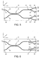
- the variations of CR as a function of Lc, associated with the wavelengths of this spectral window are sinusoids very close to each other. others, as shown in Figure 3. The more sinusoids are confused and the divider 2 to 2 is achromatic.
- the study of CR as a function of Lc makes it possible to parameterize the divisor element.
- the curves of FIG. 4 illustrate, for a divider element 2 to 2 such as that represented in FIG. 2, the total losses (including excess losses) of the light wave between the input by one of the guides and the output of this wave by one of the guides, depending on the wavelengths.
- This divider comprises in the substrate 10 a divider element 15 of type 2 to 2 such as that described with reference to FIG 2 cascaded with 2 dividing elements of type 1 to 2 which may be symmetrical or not.
- each of the output ends of the guides G1 and G2 of the element 15 is connected optically to a divider of type 1 to 2 so that the divider finally comprises two inputs referenced A1 and A2 capable of receiving a wave E and 4 outputs referenced B1, B2, B3, B4 able to output respectively a wave S1, S2 , S3, S4.
- the two dividing elements 1 to 2 are made by Y junctions referenced 21 and 23, the junction 21 is connected to the guide G1 while the junction 23 is connected to the guide G2.
- the junction 21 further comprises two output guides G'1 capable of supplying the output wave S1 and G3 capable of supplying the output wave S3;
- the junction 23 also comprises two output guides G'2 capable of supplying the output wave S2 and G4 capable of supplying the output wave S4.
- the two dividing elements 1 to 2 are formed by couplers 25 and 27.
- the coupler 25 is made by the guide G1 and a guide G5, part of which is situated in the vicinity of the guide G1 in order to couple a portion of the wave conveyed in the guide G1, in the guide G5.
- the guides G1 and G5 thus output the waves S1 and S3.
- the coupler 27 is made by the guide G2 and a guide G6, part of which is situated in the vicinity of the guide G2 in order to couple a portion of the wave conveyed in the guide G2, in the G6 guide.
- the guides G2 and G6 thus output the waves S2 and S4.
Landscapes
- Physics & Mathematics (AREA)
- General Physics & Mathematics (AREA)
- Optics & Photonics (AREA)
- Engineering & Computer Science (AREA)
- Microelectronics & Electronic Packaging (AREA)
- Optical Integrated Circuits (AREA)
- Optical Communication System (AREA)
- Glass Compositions (AREA)
- Optical Couplings Of Light Guides (AREA)
- Light Guides In General And Applications Therefor (AREA)
- Led Device Packages (AREA)
- Electrochromic Elements, Electrophoresis, Or Variable Reflection Or Absorption Elements (AREA)
- Photovoltaic Devices (AREA)
Claims (9)
- 2 x n-Leistungsteiler in integrierter Optik, wobei n eine ganze Zahl größer als oder gleich 2 ist, umfassend in einem Substrat mindestens ein optisches 2 x 2-Teilerelement (15), wobei dieses Element einen ersten und einen zweiten Leiter (G1, G2) mit Breiten W1 bzw. W2 umfasst, die in der Lage sind, eine in einen der Leiter eingeführte Eingangslichtwelle (E) in eine erste und eine zweite Ausgangswelle (S1, S2) zu teilen, die von dem ersten bzw. dem zweiten Leiter befördert werden, wobei der erste und der zweite Leiter jeweils mindestens drei Teile umfassen:- einen ersten Teil (I) von einem ersten Kopplungstyp, in dem der erste und der zweite Leiter sich allmählich bis zu einem Abstand Dc nähern, der nicht null und kleiner als ein Schwellenabstand Ds ist, der dem Minimumabstand entspricht, von dem an die in einen der Leiter eingeführte Eingangslichtwelle in der Lage ist, mindestens zum Teil in dem anderen Leiter gekoppelt zu werden,- einen zweiten Teil (II) von einem zweiten Kopplungstyp von der Länge Lc, Kopplungslänge genannt, in dem die Leiter zueinander im Wesentlichen parallel sind und um den Wert Dc beabstandet sind,- und einen dritten Teil (III) von einem ersten Kopplungstyp, in dem die Leiter sich allmählich vom Wert Dc entfernen, um einen Abstand von einem Wert von größer als Ds zu erreichen,wobei die Werte Dc, Lc, W1 und W2 so gewählt sind, dass man ein achromatisches Teilerelement bei den Betriebswellenlängen des Teilers erhält, wobei die Werte Dc und Lc so gewählt sind, dass der erste Kopplungstyp und der zweite Kopplungstyp sich mit den Wellenlängen umgekehrt ändern, dadurch gekennzeichnet, dass, wenn das 2 x 2-Teilerelement in Spektralfenstern 1260-1360 nm und 1480-1660 nm arbeitet und ein Teilungsverhältnis CR gleich 0,5 aufweist, man die Breite W1 und W2 von 1,6µm bis Wc, den Abstand Dc von 0,6 bis 2,6 µm und die Länge Lc von 0 bis 450 µm wählt, wobei Wc die Maximumbreite ist, bei der die Leiter bei diesen Spektralfenstern monomodal sind.
- Teiler nach Anspruch 1, dadurch gekennzeichnet, dass das Substrat Glas ist und die Leiter durch Ionenaustausch in dem Substrat gebildet sind.
- Teiler nach einem der Ansprüche 1 bis 2, dadurch gekennzeichnet, dass der erste und der zweite Leiter (G1, G2) solche Breiten W1 bzw. W2 aufweisen, dass das 2 x 2-Teilerelement in Berücksichtigung der Werte von Dc und Lc ein achromatisches Verhalten in den Betriebsspektralfenstern von 1260 bis 1360 nm und von 1480 bis 1660 nm aufweist.
- Teiler nach einem der Ansprüche 1 bis 3, dadurch gekennzeichnet, dass die Leiter (G1, G2) des 2 x 2-Teilerelements sich symmetrisch nähern und/oder voneinander entfernen.
- Teiler nach einem der Ansprüche 1 bis 4, dadurch gekennzeichnet, dass der Wert Dc kleiner als oder gleich einem Wert Dx ist, der dem Abstand zwischen dem ersten und dem zweiten Leiter entspricht, bei dem die Kopplung zwischen den Leitern von stark in schwach umgekehrt wird und umgekehrt, wobei die schwache Kopplung eine Kopplung bedeutet, die bei den großen Wellenlängen stärker als bei den kleinen Wellenlängen ist, und die starke Kopplung eine Kopplung bedeutet, die bei den kleinen Wellenlängen stärker als bei den großen Wellenlängen ist.
- Teiler nach einem der Ansprüche 1 bis 5, dadurch gekennzeichnet, dass in dem ersten und in dem zweiten Teil des 2 x 2-Teilerelements die Annäherung des ersten und des zweiten Leiters und/oder die Entfernung dieser Leiter voneinander gemäß einem Kreisbogen mit dem Radius R ≥ Rc oder gemäß einer Sinusfunktion stattfinden, die einen solchen Mindestkrümmungsradius R aufweist, dass R ≥ Rc, worin Rc als der kritische Krümmungsradius definiert ist, über dem es keine Krümmungsverluste bei der größten Wellenlänge der Betriebswellenlängen gibt.
- Teiler nach Anspruch 6, dadurch gekennzeichnet, dass R = Rc.
- Teiler nach einem der Ansprüche 1 bis 7, dadurch gekennzeichnet, dass, wenn n größer als 2 ist, dieser Teiler in dem Substrat ein optisches 2 x 2-Teilerelement und n-2 kaskadierte 1 x 2-Teilerelemente aufweist, so dass der Teiler 2 Eingänge, die dem ersten und dem zweiten Leiter des 2 x 2-Teilerelelements entsprechen, und n Ausgänge aufweist.
- Teiler nach Anspruch 8, dadurch gekennzeichnet, dass die n-2 1 x 2-Teilerelemente aus Kopplern und/oder Y-Verbindungen ausgewählt sind.
Applications Claiming Priority (3)
| Application Number | Priority Date | Filing Date | Title |
|---|---|---|---|
| FR0213747A FR2846755B1 (fr) | 2002-11-04 | 2002-11-04 | DIVISEUR OPTIQUE 2 VERS n EN OPTIQUE INTEGREE |
| FR0213747 | 2002-11-04 | ||
| PCT/FR2003/050111 WO2004042439A2 (fr) | 2002-11-04 | 2003-10-30 | Diviseur optique 2 vers n en optique integree |
Publications (2)
| Publication Number | Publication Date |
|---|---|
| EP1558952A2 EP1558952A2 (de) | 2005-08-03 |
| EP1558952B1 true EP1558952B1 (de) | 2006-10-04 |
Family
ID=32104402
Family Applications (1)
| Application Number | Title | Priority Date | Filing Date |
|---|---|---|---|
| EP03780301A Expired - Lifetime EP1558952B1 (de) | 2002-11-04 | 2003-10-30 | Optischer 2 x n leistungsteiler in integrierter optik |
Country Status (7)
| Country | Link |
|---|---|
| EP (1) | EP1558952B1 (de) |
| JP (1) | JP2006505812A (de) |
| AT (1) | ATE341771T1 (de) |
| DE (1) | DE60308889T2 (de) |
| ES (1) | ES2274293T3 (de) |
| FR (1) | FR2846755B1 (de) |
| WO (1) | WO2004042439A2 (de) |
Families Citing this family (4)
| Publication number | Priority date | Publication date | Assignee | Title |
|---|---|---|---|---|
| ITBL20090016A1 (it) | 2009-05-26 | 2010-11-27 | Costa Bruno | Piede in cartone ondulato per palette |
| JP5702756B2 (ja) * | 2012-08-22 | 2015-04-15 | 株式会社フジクラ | 光導波路素子 |
| JP5702757B2 (ja) * | 2012-08-22 | 2015-04-15 | 株式会社フジクラ | 光導波路素子 |
| JP5747004B2 (ja) * | 2012-08-22 | 2015-07-08 | 株式会社フジクラ | 光導波路素子 |
Family Cites Families (8)
| Publication number | Priority date | Publication date | Assignee | Title |
|---|---|---|---|---|
| US5044716A (en) * | 1989-12-08 | 1991-09-03 | Corning Incorporated | Chlorine-doped optical component |
| GB9018384D0 (en) * | 1990-08-22 | 1990-10-03 | Marconi Gec Ltd | Integrated optic waveguide coupler |
| FR2680418B1 (fr) * | 1991-08-13 | 1995-01-20 | Corning Inc | Diviseur achromatique en optique integree et coupleur de m entrees vers n sorties incorporant un tel diviseur. |
| FR2714490B1 (fr) * | 1993-12-29 | 1996-03-01 | Corning Inc | Coupleur en optique intégrée à deux entrées et 2N sorties. |
| FR2725795A1 (fr) * | 1994-10-13 | 1996-04-19 | Corning Inc | Dispositif achromatique en optique integree |
| JP2001521181A (ja) * | 1997-10-23 | 2001-11-06 | コーニング インコーポレイテッド | 断熱パルス圧縮を用いた非線形光ループミラー |
| JP2001318253A (ja) * | 2000-05-12 | 2001-11-16 | Furukawa Electric Co Ltd:The | 光導波路型方向性結合器およびこの光導波路型方向性結合器を用いた光導波回路 |
| GB0102957D0 (en) * | 2001-02-06 | 2001-03-21 | Kymata Ltd | Optical device |
-
2002
- 2002-11-04 FR FR0213747A patent/FR2846755B1/fr not_active Expired - Fee Related
-
2003
- 2003-10-30 ES ES03780301T patent/ES2274293T3/es not_active Expired - Lifetime
- 2003-10-30 WO PCT/FR2003/050111 patent/WO2004042439A2/fr not_active Ceased
- 2003-10-30 DE DE60308889T patent/DE60308889T2/de not_active Expired - Lifetime
- 2003-10-30 AT AT03780301T patent/ATE341771T1/de not_active IP Right Cessation
- 2003-10-30 JP JP2004549292A patent/JP2006505812A/ja active Pending
- 2003-10-30 EP EP03780301A patent/EP1558952B1/de not_active Expired - Lifetime
Also Published As
| Publication number | Publication date |
|---|---|
| FR2846755B1 (fr) | 2005-02-18 |
| EP1558952A2 (de) | 2005-08-03 |
| WO2004042439A3 (fr) | 2004-07-08 |
| ATE341771T1 (de) | 2006-10-15 |
| WO2004042439A2 (fr) | 2004-05-21 |
| FR2846755A1 (fr) | 2004-05-07 |
| ES2274293T3 (es) | 2007-05-16 |
| JP2006505812A (ja) | 2006-02-16 |
| DE60308889T2 (de) | 2007-04-05 |
| DE60308889D1 (de) | 2006-11-16 |
Similar Documents
| Publication | Publication Date | Title |
|---|---|---|
| EP0017571B1 (de) | Lichtintensitätsmodulator in integrierter Optik und integrierte optische Schaltung mit einem solchen Modulator | |
| EP0050059B1 (de) | Hybrid-optisches Verbindungselement und Anwendung in einem Ring-Interferometer | |
| EP3009879B1 (de) | Elektrooptischer phasenmodulator, und modulationsverfahren | |
| JP5315792B2 (ja) | 光変調器 | |
| JPH09265018A (ja) | 分岐合波光導波路回路 | |
| FR2570839A1 (fr) | Dispositif de couplage entre des guides d'onde, monolithiquement integre avec ceux-ci sur un substrat semiconducteur | |
| EP3432043A1 (de) | Optische fokalisierungsvorrichtung mit index-pseudogradienten | |
| FR2560717A1 (fr) | Resonateur multicanal a guide d'onde optique | |
| EP2664949A2 (de) | Polarisationsseparator-Optokoppler | |
| FR2680418A1 (fr) | Diviseur achromatique en optique integree et coupleur de m entrees vers n sorties incorporant un tel diviseur. | |
| FR2715232A1 (fr) | Procédé d'optimisation d'un trajet d'un guide optique et guide optique obtenu par ce procédé. | |
| EP3949042B1 (de) | Einmoden-hybrid-iii-v-auf-silizium-laser mit vereinfachtem aufbau | |
| EP1558952B1 (de) | Optischer 2 x n leistungsteiler in integrierter optik | |
| EP1433017A2 (de) | Elektrooptischer modulator, herstellungsverfahren und block zu seinem betrieb | |
| EP3513230B1 (de) | Optische kupplungsvorrichtung | |
| EP3869641A1 (de) | Abstimmbarer vernier-effekt-laser | |
| EP2260549B1 (de) | Hochleistungslaserfasersystem | |
| EP3764136B1 (de) | Verfahren zur herstellung eines adiabatischen modentransformators zwischen zwei wellenleitern | |
| JPH08503820A (ja) | リングレーザ | |
| EP0099282A1 (de) | Von der Polarisation unabhängiger integriert-optischer Modulator | |
| FR2714490A1 (fr) | Coupleur en optique intégrée à deux entrées et 2N sorties. | |
| JP2003248127A (ja) | 光パワー分割器 | |
| FR3066282A1 (fr) | Diviseur de signal optique | |
| EP2805193A1 (de) | Integrierte optische schaltung mit durchgehender abschwächungszone | |
| FR2725795A1 (fr) | Dispositif achromatique en optique integree |
Legal Events
| Date | Code | Title | Description |
|---|---|---|---|
| REG | Reference to a national code |
Ref country code: SE Ref legal event code: TRGR |
|
| PUAI | Public reference made under article 153(3) epc to a published international application that has entered the european phase |
Free format text: ORIGINAL CODE: 0009012 |
|
| 17P | Request for examination filed |
Effective date: 20050425 |
|
| AK | Designated contracting states |
Kind code of ref document: A2 Designated state(s): AT BE BG CH CY CZ DE DK EE ES FI FR GB GR HU IE IT LI LU MC NL PT RO SE SI SK TR |
|
| GRAP | Despatch of communication of intention to grant a patent |
Free format text: ORIGINAL CODE: EPIDOSNIGR1 |
|
| GRAS | Grant fee paid |
Free format text: ORIGINAL CODE: EPIDOSNIGR3 |
|
| GRAA | (expected) grant |
Free format text: ORIGINAL CODE: 0009210 |
|
| AK | Designated contracting states |
Kind code of ref document: B1 Designated state(s): AT BE BG CH CY CZ DE DK EE ES FI FR GB GR HU IE IT LI LU MC NL PT RO SE SI SK TR |
|
| PG25 | Lapsed in a contracting state [announced via postgrant information from national office to epo] |
Ref country code: IT Free format text: LAPSE BECAUSE OF FAILURE TO SUBMIT A TRANSLATION OF THE DESCRIPTION OR TO PAY THE FEE WITHIN THE PRESCRIBED TIME-LIMIT;WARNING: LAPSES OF ITALIAN PATENTS WITH EFFECTIVE DATE BEFORE 2007 MAY HAVE OCCURRED AT ANY TIME BEFORE 2007. THE CORRECT EFFECTIVE DATE MAY BE DIFFERENT FROM THE ONE RECORDED. Effective date: 20061004 Ref country code: AT Free format text: LAPSE BECAUSE OF FAILURE TO SUBMIT A TRANSLATION OF THE DESCRIPTION OR TO PAY THE FEE WITHIN THE PRESCRIBED TIME-LIMIT Effective date: 20061004 Ref country code: CZ Free format text: LAPSE BECAUSE OF FAILURE TO SUBMIT A TRANSLATION OF THE DESCRIPTION OR TO PAY THE FEE WITHIN THE PRESCRIBED TIME-LIMIT Effective date: 20061004 Ref country code: RO Free format text: LAPSE BECAUSE OF FAILURE TO SUBMIT A TRANSLATION OF THE DESCRIPTION OR TO PAY THE FEE WITHIN THE PRESCRIBED TIME-LIMIT Effective date: 20061004 Ref country code: IE Free format text: LAPSE BECAUSE OF FAILURE TO SUBMIT A TRANSLATION OF THE DESCRIPTION OR TO PAY THE FEE WITHIN THE PRESCRIBED TIME-LIMIT Effective date: 20061004 Ref country code: SI Free format text: LAPSE BECAUSE OF FAILURE TO SUBMIT A TRANSLATION OF THE DESCRIPTION OR TO PAY THE FEE WITHIN THE PRESCRIBED TIME-LIMIT Effective date: 20061004 Ref country code: NL Free format text: LAPSE BECAUSE OF FAILURE TO SUBMIT A TRANSLATION OF THE DESCRIPTION OR TO PAY THE FEE WITHIN THE PRESCRIBED TIME-LIMIT Effective date: 20061004 Ref country code: FI Free format text: LAPSE BECAUSE OF FAILURE TO SUBMIT A TRANSLATION OF THE DESCRIPTION OR TO PAY THE FEE WITHIN THE PRESCRIBED TIME-LIMIT Effective date: 20061004 Ref country code: SK Free format text: LAPSE BECAUSE OF FAILURE TO SUBMIT A TRANSLATION OF THE DESCRIPTION OR TO PAY THE FEE WITHIN THE PRESCRIBED TIME-LIMIT Effective date: 20061004 |
|
| REG | Reference to a national code |
Ref country code: GB Ref legal event code: FG4D Free format text: NOT ENGLISH |
|
| PG25 | Lapsed in a contracting state [announced via postgrant information from national office to epo] |
Ref country code: MC Free format text: LAPSE BECAUSE OF NON-PAYMENT OF DUE FEES Effective date: 20061031 |
|
| REG | Reference to a national code |
Ref country code: CH Ref legal event code: EP |
|
| PGFP | Annual fee paid to national office [announced via postgrant information from national office to epo] |
Ref country code: FR Payment date: 20061107 Year of fee payment: 4 |
|
| REG | Reference to a national code |
Ref country code: IE Ref legal event code: FG4D Free format text: LANGUAGE OF EP DOCUMENT: FRENCH |
|
| REF | Corresponds to: |
Ref document number: 60308889 Country of ref document: DE Date of ref document: 20061116 Kind code of ref document: P |
|
| PG25 | Lapsed in a contracting state [announced via postgrant information from national office to epo] |
Ref country code: BG Free format text: LAPSE BECAUSE OF FAILURE TO SUBMIT A TRANSLATION OF THE DESCRIPTION OR TO PAY THE FEE WITHIN THE PRESCRIBED TIME-LIMIT Effective date: 20070104 Ref country code: DK Free format text: LAPSE BECAUSE OF FAILURE TO SUBMIT A TRANSLATION OF THE DESCRIPTION OR TO PAY THE FEE WITHIN THE PRESCRIBED TIME-LIMIT Effective date: 20070104 |
|
| GBT | Gb: translation of ep patent filed (gb section 77(6)(a)/1977) |
Effective date: 20061220 |
|
| PG25 | Lapsed in a contracting state [announced via postgrant information from national office to epo] |
Ref country code: PT Free format text: LAPSE BECAUSE OF FAILURE TO SUBMIT A TRANSLATION OF THE DESCRIPTION OR TO PAY THE FEE WITHIN THE PRESCRIBED TIME-LIMIT Effective date: 20070316 |
|
| NLV1 | Nl: lapsed or annulled due to failure to fulfill the requirements of art. 29p and 29m of the patents act | ||
| REG | Reference to a national code |
Ref country code: ES Ref legal event code: FG2A Ref document number: 2274293 Country of ref document: ES Kind code of ref document: T3 Ref country code: IE Ref legal event code: FD4D |
|
| PLBE | No opposition filed within time limit |
Free format text: ORIGINAL CODE: 0009261 |
|
| STAA | Information on the status of an ep patent application or granted ep patent |
Free format text: STATUS: NO OPPOSITION FILED WITHIN TIME LIMIT |
|
| 26N | No opposition filed |
Effective date: 20070705 |
|
| BERE | Be: lapsed |
Owner name: TEEM PHOTONICS Effective date: 20061031 |
|
| PG25 | Lapsed in a contracting state [announced via postgrant information from national office to epo] |
Ref country code: GR Free format text: LAPSE BECAUSE OF FAILURE TO SUBMIT A TRANSLATION OF THE DESCRIPTION OR TO PAY THE FEE WITHIN THE PRESCRIBED TIME-LIMIT Effective date: 20070105 |
|
| REG | Reference to a national code |
Ref country code: CH Ref legal event code: PL |
|
| PG25 | Lapsed in a contracting state [announced via postgrant information from national office to epo] |
Ref country code: EE Free format text: LAPSE BECAUSE OF FAILURE TO SUBMIT A TRANSLATION OF THE DESCRIPTION OR TO PAY THE FEE WITHIN THE PRESCRIBED TIME-LIMIT Effective date: 20061004 |
|
| PG25 | Lapsed in a contracting state [announced via postgrant information from national office to epo] |
Ref country code: LI Free format text: LAPSE BECAUSE OF NON-PAYMENT OF DUE FEES Effective date: 20071031 Ref country code: HU Free format text: LAPSE BECAUSE OF FAILURE TO SUBMIT A TRANSLATION OF THE DESCRIPTION OR TO PAY THE FEE WITHIN THE PRESCRIBED TIME-LIMIT Effective date: 20070405 Ref country code: TR Free format text: LAPSE BECAUSE OF FAILURE TO SUBMIT A TRANSLATION OF THE DESCRIPTION OR TO PAY THE FEE WITHIN THE PRESCRIBED TIME-LIMIT Effective date: 20061004 Ref country code: CH Free format text: LAPSE BECAUSE OF NON-PAYMENT OF DUE FEES Effective date: 20071031 Ref country code: LU Free format text: LAPSE BECAUSE OF NON-PAYMENT OF DUE FEES Effective date: 20061030 |
|
| REG | Reference to a national code |
Ref country code: FR Ref legal event code: ST Effective date: 20080630 |
|
| PG25 | Lapsed in a contracting state [announced via postgrant information from national office to epo] |
Ref country code: CY Free format text: LAPSE BECAUSE OF FAILURE TO SUBMIT A TRANSLATION OF THE DESCRIPTION OR TO PAY THE FEE WITHIN THE PRESCRIBED TIME-LIMIT Effective date: 20061004 |
|
| PG25 | Lapsed in a contracting state [announced via postgrant information from national office to epo] |
Ref country code: FR Free format text: LAPSE BECAUSE OF NON-PAYMENT OF DUE FEES Effective date: 20071031 |
|
| PG25 | Lapsed in a contracting state [announced via postgrant information from national office to epo] |
Ref country code: BE Free format text: LAPSE BECAUSE OF FAILURE TO SUBMIT A TRANSLATION OF THE DESCRIPTION OR TO PAY THE FEE WITHIN THE PRESCRIBED TIME-LIMIT Effective date: 20061031 |
|
| PGFP | Annual fee paid to national office [announced via postgrant information from national office to epo] |
Ref country code: IT Payment date: 20151014 Year of fee payment: 13 |
|
| PGFP | Annual fee paid to national office [announced via postgrant information from national office to epo] |
Ref country code: SE Payment date: 20151014 Year of fee payment: 13 Ref country code: ES Payment date: 20151026 Year of fee payment: 13 |
|
| PG25 | Lapsed in a contracting state [announced via postgrant information from national office to epo] |
Ref country code: SE Free format text: LAPSE BECAUSE OF NON-PAYMENT OF DUE FEES Effective date: 20161031 |
|
| PG25 | Lapsed in a contracting state [announced via postgrant information from national office to epo] |
Ref country code: IT Free format text: LAPSE BECAUSE OF NON-PAYMENT OF DUE FEES Effective date: 20161030 |
|
| PG25 | Lapsed in a contracting state [announced via postgrant information from national office to epo] |
Ref country code: ES Free format text: LAPSE BECAUSE OF NON-PAYMENT OF DUE FEES Effective date: 20161031 |
|
| REG | Reference to a national code |
Ref country code: ES Ref legal event code: FD2A Effective date: 20181122 |
|
| PGFP | Annual fee paid to national office [announced via postgrant information from national office to epo] |
Ref country code: DE Payment date: 20211110 Year of fee payment: 19 Ref country code: GB Payment date: 20211122 Year of fee payment: 19 |
|
| REG | Reference to a national code |
Ref country code: DE Ref legal event code: R119 Ref document number: 60308889 Country of ref document: DE |
|
| GBPC | Gb: european patent ceased through non-payment of renewal fee |
Effective date: 20221030 |
|
| PG25 | Lapsed in a contracting state [announced via postgrant information from national office to epo] |
Ref country code: DE Free format text: LAPSE BECAUSE OF NON-PAYMENT OF DUE FEES Effective date: 20230503 |
|
| PG25 | Lapsed in a contracting state [announced via postgrant information from national office to epo] |
Ref country code: GB Free format text: LAPSE BECAUSE OF NON-PAYMENT OF DUE FEES Effective date: 20221030 |