EP1557561A1 - Booster power supply for engine generator and its controlling method - Google Patents
Booster power supply for engine generator and its controlling method Download PDFInfo
- Publication number
- EP1557561A1 EP1557561A1 EP03738607A EP03738607A EP1557561A1 EP 1557561 A1 EP1557561 A1 EP 1557561A1 EP 03738607 A EP03738607 A EP 03738607A EP 03738607 A EP03738607 A EP 03738607A EP 1557561 A1 EP1557561 A1 EP 1557561A1
- Authority
- EP
- European Patent Office
- Prior art keywords
- voltage
- circuit
- converter
- boosting
- engine
- Prior art date
- Legal status (The legal status is an assumption and is not a legal conclusion. Google has not performed a legal analysis and makes no representation as to the accuracy of the status listed.)
- Granted
Links
Images


Classifications
-
- F—MECHANICAL ENGINEERING; LIGHTING; HEATING; WEAPONS; BLASTING
- F02—COMBUSTION ENGINES; HOT-GAS OR COMBUSTION-PRODUCT ENGINE PLANTS
- F02P—IGNITION, OTHER THAN COMPRESSION IGNITION, FOR INTERNAL-COMBUSTION ENGINES; TESTING OF IGNITION TIMING IN COMPRESSION-IGNITION ENGINES
- F02P15/00—Electric spark ignition having characteristics not provided for in, or of interest apart from, groups F02P1/00 - F02P13/00 and combined with layout of ignition circuits
- F02P15/12—Electric spark ignition having characteristics not provided for in, or of interest apart from, groups F02P1/00 - F02P13/00 and combined with layout of ignition circuits having means for strengthening spark during starting
-
- H—ELECTRICITY
- H02—GENERATION; CONVERSION OR DISTRIBUTION OF ELECTRIC POWER
- H02M—APPARATUS FOR CONVERSION BETWEEN AC AND AC, BETWEEN AC AND DC, OR BETWEEN DC AND DC, AND FOR USE WITH MAINS OR SIMILAR POWER SUPPLY SYSTEMS; CONVERSION OF DC OR AC INPUT POWER INTO SURGE OUTPUT POWER; CONTROL OR REGULATION THEREOF
- H02M3/00—Conversion of DC power input into DC power output
- H02M3/02—Conversion of DC power input into DC power output without intermediate conversion into AC
- H02M3/04—Conversion of DC power input into DC power output without intermediate conversion into AC by static converters
- H02M3/10—Conversion of DC power input into DC power output without intermediate conversion into AC by static converters using discharge tubes with control electrode or semiconductor devices with control electrode
- H02M3/145—Conversion of DC power input into DC power output without intermediate conversion into AC by static converters using discharge tubes with control electrode or semiconductor devices with control electrode using devices of a triode or transistor type requiring continuous application of a control signal
- H02M3/155—Conversion of DC power input into DC power output without intermediate conversion into AC by static converters using discharge tubes with control electrode or semiconductor devices with control electrode using devices of a triode or transistor type requiring continuous application of a control signal using semiconductor devices only
- H02M3/156—Conversion of DC power input into DC power output without intermediate conversion into AC by static converters using discharge tubes with control electrode or semiconductor devices with control electrode using devices of a triode or transistor type requiring continuous application of a control signal using semiconductor devices only with automatic control of output voltage or current, e.g. switching regulators
-
- B—PERFORMING OPERATIONS; TRANSPORTING
- B60—VEHICLES IN GENERAL
- B60R—VEHICLES, VEHICLE FITTINGS, OR VEHICLE PARTS, NOT OTHERWISE PROVIDED FOR
- B60R16/00—Electric or fluid circuits specially adapted for vehicles and not otherwise provided for; Arrangement of elements of electric or fluid circuits specially adapted for vehicles and not otherwise provided for
- B60R16/02—Electric or fluid circuits specially adapted for vehicles and not otherwise provided for; Arrangement of elements of electric or fluid circuits specially adapted for vehicles and not otherwise provided for electric constitutive elements
- B60R16/03—Electric or fluid circuits specially adapted for vehicles and not otherwise provided for; Arrangement of elements of electric or fluid circuits specially adapted for vehicles and not otherwise provided for electric constitutive elements for supply of electrical power to vehicle subsystems or for
-
- F—MECHANICAL ENGINEERING; LIGHTING; HEATING; WEAPONS; BLASTING
- F02—COMBUSTION ENGINES; HOT-GAS OR COMBUSTION-PRODUCT ENGINE PLANTS
- F02N—STARTING OF COMBUSTION ENGINES; STARTING AIDS FOR SUCH ENGINES, NOT OTHERWISE PROVIDED FOR
- F02N3/00—Other muscle-operated starting apparatus
- F02N3/04—Other muscle-operated starting apparatus having foot-actuated levers
-
- F—MECHANICAL ENGINEERING; LIGHTING; HEATING; WEAPONS; BLASTING
- F02—COMBUSTION ENGINES; HOT-GAS OR COMBUSTION-PRODUCT ENGINE PLANTS
- F02P—IGNITION, OTHER THAN COMPRESSION IGNITION, FOR INTERNAL-COMBUSTION ENGINES; TESTING OF IGNITION TIMING IN COMPRESSION-IGNITION ENGINES
- F02P3/00—Other installations
- F02P3/06—Other installations having capacitive energy storage
- F02P3/08—Layout of circuits
- F02P3/0876—Layout of circuits the storage capacitor being charged by means of an energy converter (DC-DC converter) or of an intermediate storage inductance
- F02P3/0884—Closing the discharge circuit of the storage capacitor with semiconductor devices
- F02P3/0892—Closing the discharge circuit of the storage capacitor with semiconductor devices using digital techniques
-
- H—ELECTRICITY
- H02—GENERATION; CONVERSION OR DISTRIBUTION OF ELECTRIC POWER
- H02M—APPARATUS FOR CONVERSION BETWEEN AC AND AC, BETWEEN AC AND DC, OR BETWEEN DC AND DC, AND FOR USE WITH MAINS OR SIMILAR POWER SUPPLY SYSTEMS; CONVERSION OF DC OR AC INPUT POWER INTO SURGE OUTPUT POWER; CONTROL OR REGULATION THEREOF
- H02M1/00—Details of apparatus for conversion
- H02M1/0003—Details of control, feedback or regulation circuits
- H02M1/0016—Control circuits providing compensation of output voltage deviations using feedforward of disturbance parameters
- H02M1/0022—Control circuits providing compensation of output voltage deviations using feedforward of disturbance parameters the disturbance parameters being input voltage fluctuations
Definitions
- the present invention relates to a voltage booster for engine generator and control method thereof.
- a motor bicycle uses as an engine start ignition circuit the CDI (capacitor discharge igniter) method and the full transistor igniter method.
- the CDI can operate regardless of presence/absence of a battery and can perform engine start by a so-called kick method.
- the CDI has a problem that it is inferior to the full transistor igniter method when igniting a dilute air-fuel mixture.
- the full transistor igniter method is appropriate for energy saving such as optimal ignition control of engine but requires a battery and cannot start an engine by the kick method.
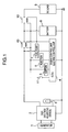
- the full transistor igniter circuit includes a generator 1, a voltage adjusting unit 2, a battery 8, a lamp 3, an engine control unit (ECU) 4, an igniter 5, an injector 6, a fuel pump 7, and other DC load 9 connected in parallel.
- ECU engine control unit
- an igniter 5 an injector 6, a fuel pump 7, and other DC load 9 connected in parallel.
- a main switch 11 is such as a starter button is closed, voltage from the battery 8 is supplied to the entire circuit to operate the ECU 4 and relays 10, 40 are closed to start the engine.
- the voltage booster for engine generator in order to achieve the aforementioned object, between a voltage adjusting device receiving a start current from the generator driven by the kick method and a load such as an ECU connected to the voltage adjusting device, there is connected an active boosting circuit for boosting voltage while the voltage adjusting device outputs a low voltage upon engine start by the kick method and terminating the boosting operation when the stationary operation is set in after the engine start. Only upon engine start, the output of the voltage adjusting device is boosted by the active boosting circuit and supplied to a load such as the ECU.
- the present invention provides a control method for the voltage booster for engine generator.
- the voltage booster for engine generator including a load such as an ECU connected to a voltage adjusting device receiving a start current from the generator driven by the kick method, the output voltage output from the voltage adjusting device is compared to the operation voltage of the engine stationary operation and boosting adjustment is performed until the output voltage reaches the operation voltage of the stationary operation.
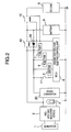
- Fig. 2 shows the entire configuration of the voltage booster for engine generator according to the present invention.
- the voltage booster for engine generator of Fig. 2 is characterized in that the DC/DC converter 20 is connected as an active booster circuit between the voltage adjustment unit (REG) 2 and the electronic device such as the ECU 4 connected to the REG 2 to receive voltage.
- the battery 8 shown in the figure is in the discharge state below a predetermined start voltage upon start by the kick method as an object of the present invention and it is assumed that the generator 1 is driven by the so-called kick method. After the engine reaches a stationary rotation, the battery 8 is charged and afterwards, the engine can be started by the battery 8.
- a diode 39 is inserted between the DC/DC converter 20 and the battery 8, so as to prevent flow in of current to the side of the battery 8 having a large current capacity upon boosting of the DC/DC converter 20.
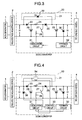
- Fig. 3 shows detailed configuration of this DC/DC converter 20.
- the DC/DC converter basically consists of a diode 23, a coil 24, and a diode 25 which are connected in series and a capacitor 26, a transistor 27, and a capacitor 30 which are connected between the series connection and the ground line.
- a bypass circuit 21 consisting of a diode 22 connected in parallel between the diodes 23 and 25 is provided. Furthermore, a feedback circuit 32 including a Zener diode 30 is arranged. Furthermore, the output of the feedback circuit 32 is connected to an oscillation circuit 31. This oscillation circuit 31 is configured so as to supply a drive signal to the base of the transistor 27 via a resistor 28.
- the control voltage V1 of the REG 2 (output fluctuating depending on the rpm of the generator) is compared to the control voltage V2 of the DC/DC converter 20 (a reference voltage such as 12V at which the engine performs stationary rotation and the electronic devices operate normally). That is, when the control voltage V1 of the REG 2 by a low rpm at rotation start by turning on the main switch 11 and kicking the ACG 1 is lower than the control voltage V2 of the DC/DC converter 20 (V1 ⁇ V2), the voltage value passing through the bypass circuit 21 and subtracted by the voltage drop by the diode 22 (V1 - voltage drop of diode) is applied.
- the voltage value detected is input to the feedback circuit 32 and the relationship of V1 ⁇ V2 is recognized.
- the feedback circuit outputs a feedback signal corresponding to the difference between the V1 and V2 to the oscillation circuit 31 so as to drive the oscillation circuit 31.
- the oscillation circuit 31 sends a corresponding drive signal to the base of the transistor 27 via the resistor 28.
- the transistor 27 is conducted/controlled and the DC/DC converter 20 operates to boost the voltage from the current V1 to the control voltage V2 which is a reference voltage.
- the ECU 4 When the reference voltage V2 boosted by the DC/DC converter 20 is output, the ECU 4 operates and the engine starts operation. With this engine start, the ACG 1 is driven by the engine to increase the rpm. When the ACG 1 reaches the stationary rotation, the voltage applied to the Zener diode 30 via the bypass circuit 21 is increased step by step to a value equal to or above V2 when subtracted by the voltage drop of the diode 22. At this moment, a voltage equal to or above 2V which is the preset output of the DC/DC convert 20 is detected by the feedback circuit 32 (V1 > V2).
- the feedback circuit 32 transmits a feedback signal so as to stop drive output of the oscillation circuit 31 to the transistor 27.
- the boosting operation of the DC/DC converter 20 stops.
- the control voltage V1 of the REG 2 which has become equal to or above the control voltage V2 of the DC/DC converter 20 is bypassed by the diode 22 of the bypass circuit 21 and supplied dto the electronic circuits such as the ECU 4.
- the relays 10, 40 are closed and a reference voltage is applied to the DC load 9, thereby starting charge of the battery 8.
- the engine performs stationary rotation and the ACG 1 generates above the nominal output.
- the output voltage of the stationary operation is obtained and supplied via the bypass circuit 21 to the ECU 4 and other electronic devices.
- the bypass circuit 21 is composed of a diode but it can also be replaced by a resistor.
- the oscillation circuit 31 may be configured to oscillate stationary drive frequency such as 50 KHz and cut off the DC/DC converter circuit by the relay using a signal of the feedback circuit 32 instead of using control of PWM and PFM.
- the bypass circuit 21 is composed of a relay 34 and a control circuit 34 is provided to operate the relay 34.
- This control circuit 33 includes a Zener diode 38 for monitoring voltage V1 arranged at the input side of the DC/DC converter 20.
- this control circuit 33 may be replaced by a timer circuit controlling ON/OFF of the relay 34 after a sufficient time when the V1 becomes greater than V2 after the start by the kick method, or may be replaced by a switching element such as a transistor. Moreover, it is possible to turn ON/OFF when the value of V1 reaches the stationary rotation value regardless of the value of V2.
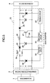
- a relay 34 is provided at the input side of the diode 23 instead of the bypass circuit 21, so as to be operated by the control circuit 33 similar to the one in Fig. 4.
- the engine is normally started by the kick when the relay 34 is closed.
- the control circuit 323 operates to open the relay 34, so that the DC/DC converter 20 itself enters a stop state.
- V1 equal to or greater than V2 is supplied to the electronic devices such as ECU 5 connected in parallel to the REG 2 and the operation is maintained.
- the control circuit 33 monitors the control voltage V2 of the DC/DC converter, or it may be replaced by a timer operating after a lapse of a predetermined period of time.
- the relay may be replaced by the switching element such as a transistor.
- the engine performs the stationary operation and the stationary voltage from the REG 2 obtained by the stationary operation of the engine closes the relay 10, so that the stationary voltage is applied to all the circuit components shown in Fig. 2.
- the oscillation circuit 31 boosts the control voltage V1 from the REG 2 to a predetermined voltage V2 by the feedback signal from the feedback circuit 32. Furthermore, an oscillation circuit 35 consisting of a resistor 36 and a transistor 37 is provided for terminating the operation of the transistor 27. This oscillation stop circuit 35 is controlled by a control circuit 33 having a Zener diode 38 for detecting the voltage V1 of the input side of the DC/DC converter 20.
- the control circuit 33 terminates the operation of the transistor 27 under the condition of V1 ⁇ V2 in the same way as the embodiment of Fig. 3 and substantially terminates the operation of the DC/DC converter 20.
- the control circuit 33 may directly monitor the voltage V1 or timer operation can be used to terminate the oscillation stop circuit 35. In this configuration also, it is possible to employ a relay operating upon a voltage of stationary rotation regardless of the value of V2.
- the oscillation circuit 31 performs feedback control by the feedback circuit 32 and a bypass circuit 21 consisting of a diode 22 is provided in parallel.
- the feedback circuit 32 monitors the control voltage V1 of the REG 2 and upon detection of V1 > V2, the control circuit 33 operates the oscillation stop circuit 35.
- the engine after stop of bossing operation of the DC/DC converter 20, the engine performs stationary operation and the stationary voltage from the REG 2 operates the oscillation stop circuit 35, so that the stationary voltage is applied to all the circuit components shown in Fig. 2.
- this configuration also, it is possible to use an oscillation stop circuit operating upon a voltage of the stationary rotation regardless of the value of V2.
- the voltage booster for engine generator and control method thereof enables the engine ignition circuit of the full transistor igniter method to start the engine by the so-called kick method even when the battery is in a discharge state.
Landscapes
- Engineering & Computer Science (AREA)
- Power Engineering (AREA)
- Chemical & Material Sciences (AREA)
- Combustion & Propulsion (AREA)
- Mechanical Engineering (AREA)
- General Engineering & Computer Science (AREA)
- Ignition Installations For Internal Combustion Engines (AREA)
- Dc-Dc Converters (AREA)
- Electrical Control Of Ignition Timing (AREA)
- Control Of Eletrric Generators (AREA)
Abstract
Description
Claims (11)
- A voltage booster for an engine generator which is an engine ignition apparatus of the full transistor igniter method, comprising:a generator which can be driven by the kick method,a voltage adjusting device connected to the generator and adjusting voltage of power supplied from the generator,an electronic device connected to the voltage adjusting device and controlling ignition/operation control of the engine by voltage supplied from the voltage adjusting device, andan active boosting circuit connected between the voltage adjusting device and the electronic device, boosting the output voltage of the voltage adjusting device to a predetermined nominal voltage of the electronic device upon the engine start by kicking the generator when the power supply is lower than the predetermined engine stationary operation, and stopping the boosting operation when the output voltage from the voltage adjusting device has become the predetermined nominal voltage of the engine stationary operation.
- A voltage booster for engine generator as claimed in Claim 1, wherein the active boosting circuit is a DC/DC converter having:a feedback circuit for performing feedback so that the voltage of the output side becomes the predetermined nominal voltage, anda bypass circuit for bypassing from the input side to the output side of the active boosting circuit by a predetermined voltage drop,and the feedback circuit stops boosting operation of the DC/DC converter when the voltage V1 of the input side bypassed to the output side of the DC/DC converter which is subtracted by voltage drop of the bypass circuit exceeds a predetermined nominal voltage V2 (V1 - voltage drop of bypass circuit > V2).
- A voltage booster for engine generator as claimed in Claim 1, wherein the active boosting circuit is a DC/DC converter having:a feedback circuit for performing feedback so that the voltage of the output side becomes the predetermined nominal voltage,a bypass circuit having a relay which is normally open and bypassing from the input side to the output side of the active boosting circuit, anda control circuit for detecting the voltage of the input side of the active boosting circuit and closing the relay which is normally open,and at the moment when the voltage V1 of the input side has become a predetermined voltage from the voltage adjusting device during the stationary operation, the control circuit closes the relay so as to stop the boosting operation of the DC/DC converter.
- A voltage booster for engine generator as claimed in Claim 3, wherein the moment of the predetermined voltage is a moment when the predetermined nominal voltage V2 is exceeded (V1 > V2), and the relay is closed at this moment, and the feedback circuit stops the boosting operation of the DC/DC converter when the voltage V1 of the input side bypassed by the output side of the DC/DC converter exceeds the predetermined nominal voltage (V1 > V2).
- A voltage booster for engine generator as claimed in Claim 1, wherein the active boosting circuit is a DC/DC converter having:a feedback circuit for performing feedback so that the voltage of the output side becomes the predetermined nominal voltage,a relay which is provided at the input side and normally closed, anda control circuit for operating the relay according to the voltage V1 at the input side of the active boosting circuit,and the control circuit opens the relay at the moment when the voltage V1 of the input side has become a predetermined voltage from the voltage adjusting device during stationary operation so as to stop the boosting operation of the DC/DC converter.
- A voltage booster for engine generator as claimed in Claim 5, wherein the moment when the predetermined voltage is obtained is the moment when the voltage has become equal to or above the nominal voltage V2 (V1 ≥ V2) and at this moment the relay is opened.
- A voltage booster for engine generator as claimed in Claim 6, wherein the active boosting circuit is a DC/DC converter having:a feedback circuit for performing feedback so that the voltage of the output side is the predetermined nominal voltage V2, anda control circuit for detecting the voltage V1 of the input side of the active boosting side so as to stop the boosting operation,and at the moment when the voltage V1 of the input side has become a predetermined voltage from the voltage adjusting device during the stationary operation, the control circuit stops the oscillation stop circuit and stops the boosting operation of the DC/DC converter.
- A voltage booster for engine generator as claimed in Claim 7, wherein the moment when the predetermined voltage is obtained is the moment when the voltage is equal to or above the nominal voltage (V1 ≥ V2) and at this moment operation of the DC/DC converter is stopped.
- A voltage booster for engine generator as claimed in Claim 1, wherein the active boosting circuit is a DC/DC converter having:a feedback circuit for performing feedback so that the voltage of the output side becomes the predetermined nominal voltage V2,a bypass circuit bypassing from the input side to the output side of the active boosting circuit by a predetermined voltage drop, anda control circuit for terminating operation of the active boosting circuit by the output of the feedback circuit,and at the moment when the voltage V1 of the input side bypassed to the output side has become a predetermined voltage from the voltage adjusting device during the stationary operation, the feedback circuit stops the boosting operation of the DC/DC converter.
- A voltage booster for engine generator as claimed in Claim 9, wherein the predetermined moment is the moment when the voltage has exceeded the nominal voltage V2 and at this moment boosting operation of the DC/DC converter is stopped.
- An ignition control method for an engine ignition apparatus of the full transistor igniter method having a battery and a generator which can be driven by the kick method, the method comprising steps of:boosting voltage driven by a kick to a predetermined nominal voltage of the stationary operation of the ignition apparatus while a low voltage of a generator insufficient for engine stationary operation is output and applying the boosted voltage to the ignition apparatus, andterminating the boosting operation when the voltage has become equal to or above the voltage of stationary operation and applying the output voltage of the generator directly to the ignition apparatus.
Applications Claiming Priority (3)
| Application Number | Priority Date | Filing Date | Title |
|---|---|---|---|
| JP2002194897 | 2002-07-03 | ||
| JP2002194897A JP4209640B2 (en) | 2002-07-03 | 2002-07-03 | Boost power supply for engine generator |
| PCT/JP2003/008358 WO2004005705A1 (en) | 2002-07-03 | 2003-07-01 | Booster power supply for engine generator and its controlling method |
Publications (3)
| Publication Number | Publication Date |
|---|---|
| EP1557561A1 true EP1557561A1 (en) | 2005-07-27 |
| EP1557561A4 EP1557561A4 (en) | 2009-04-08 |
| EP1557561B1 EP1557561B1 (en) | 2017-12-06 |
Family
ID=30112317
Family Applications (1)
| Application Number | Title | Priority Date | Filing Date |
|---|---|---|---|
| EP03738607.5A Expired - Lifetime EP1557561B1 (en) | 2002-07-03 | 2003-07-01 | Booster power supply for engine generator and its controlling method |
Country Status (5)
| Country | Link |
|---|---|
| EP (1) | EP1557561B1 (en) |
| JP (1) | JP4209640B2 (en) |
| CN (1) | CN1316725C (en) |
| BR (1) | BR0312279A (en) |
| WO (1) | WO2004005705A1 (en) |
Cited By (5)
| Publication number | Priority date | Publication date | Assignee | Title |
|---|---|---|---|---|
| EP1876694A1 (en) * | 2006-07-03 | 2008-01-09 | Siemens Aktiengesellschaft | Booster circuit |
| FR2904157A1 (en) * | 2006-07-24 | 2008-01-25 | Valeo Sys Controle Moteur Sas | POWER SUPPLY CIRCUIT OF A CONTROL MODULE HAVING TWO POWER MODES |
| WO2010094397A1 (en) | 2009-02-20 | 2010-08-26 | Continental Automotive France | Computer of an automobile comprising a voltage step-up device and control method |
| DE102013206312B4 (en) | 2012-04-25 | 2021-07-29 | Denso Corporation | Electronic in-vehicle control system |
| US11319915B2 (en) | 2020-06-11 | 2022-05-03 | Kohler Co. | Engine system, and method of starting the engine |
Families Citing this family (8)
| Publication number | Priority date | Publication date | Assignee | Title |
|---|---|---|---|---|
| JP5024963B2 (en) | 2008-07-23 | 2012-09-12 | オムロンオートモーティブエレクトロニクス株式会社 | Engine starter |
| US7938092B2 (en) * | 2009-06-19 | 2011-05-10 | Tai-Her Yang | Combustion and emergency starting control system with auxiliary power |
| US8490593B2 (en) * | 2009-06-19 | 2013-07-23 | Tai-Her Yang | Split-type auxiliary power combustion and emergency starting system |
| DE102013218227A1 (en) | 2012-09-12 | 2014-05-28 | Robert Bosch Gmbh | Ignition system for an internal combustion engine |
| EP2895734B1 (en) | 2012-09-12 | 2019-03-27 | Robert Bosch GmbH | Ignition system for an internal combustion engine |
| CN102979656A (en) * | 2012-12-10 | 2013-03-20 | 南京航空航天大学 | Self-adaptive high energy ignition system |
| DE102016207132B4 (en) * | 2016-04-27 | 2020-06-04 | Continental Automotive Gmbh | Method and circuit device for stabilizing an electrical system voltage |
| JP2019154129A (en) * | 2018-03-02 | 2019-09-12 | パナソニックIpマネジメント株式会社 | Mobile body power supply device and mobile body using the same |
Family Cites Families (12)
| Publication number | Priority date | Publication date | Assignee | Title |
|---|---|---|---|---|
| JPS51132339A (en) * | 1974-12-30 | 1976-11-17 | Yoshio Fujino | Auxiliary power source device for starting of firework ignition type e ngine |
| JPS58143165A (en) * | 1982-02-19 | 1983-08-25 | Automob Antipollut & Saf Res Center | Ignition system for internal-combustion engine |
| JPH0322551Y2 (en) * | 1984-09-07 | 1991-05-16 | ||
| JPH01224474A (en) * | 1988-03-01 | 1989-09-07 | Mitsubishi Electric Corp | Engine control device |
| JPH0750985B2 (en) * | 1989-06-29 | 1995-05-31 | 阪神エレクトリック株式会社 | DC-DC converter |
| JPH04132877A (en) * | 1990-09-21 | 1992-05-07 | Yamaha Motor Co Ltd | Starting device for motorcycle |
| JP2749746B2 (en) * | 1992-11-18 | 1998-05-13 | 三菱電機株式会社 | Internal combustion engine ignition device |
| JPH06229312A (en) * | 1993-02-01 | 1994-08-16 | Toyota Motor Corp | Controller of internal combustion engine |
| JP3722567B2 (en) * | 1996-09-19 | 2005-11-30 | 株式会社ミツバ | Ignition control device |
| CN1245867A (en) * | 1998-08-25 | 2000-03-01 | 郭建国 | Method for producing high-voltage ignition for automobile and its equipment |
| JP3889212B2 (en) * | 2000-09-25 | 2007-03-07 | 本田技研工業株式会社 | Generator voltage boosting method |
| JP2002256962A (en) * | 2001-02-26 | 2002-09-11 | Mikuni Corp | Power supply for internal combustion engine |
-
2002
- 2002-07-03 JP JP2002194897A patent/JP4209640B2/en not_active Expired - Fee Related
-
2003
- 2003-07-01 EP EP03738607.5A patent/EP1557561B1/en not_active Expired - Lifetime
- 2003-07-01 WO PCT/JP2003/008358 patent/WO2004005705A1/en not_active Ceased
- 2003-07-01 CN CNB038191652A patent/CN1316725C/en not_active Expired - Fee Related
- 2003-07-01 BR BR0312279-4A patent/BR0312279A/en not_active Application Discontinuation
Cited By (10)
| Publication number | Priority date | Publication date | Assignee | Title |
|---|---|---|---|---|
| EP1876694A1 (en) * | 2006-07-03 | 2008-01-09 | Siemens Aktiengesellschaft | Booster circuit |
| FR2904157A1 (en) * | 2006-07-24 | 2008-01-25 | Valeo Sys Controle Moteur Sas | POWER SUPPLY CIRCUIT OF A CONTROL MODULE HAVING TWO POWER MODES |
| WO2008012430A3 (en) * | 2006-07-24 | 2008-03-20 | Valeo Sys Controle Moteur Sas | Electric circuit for powering a control module comprising two powering modes |
| WO2010094397A1 (en) | 2009-02-20 | 2010-08-26 | Continental Automotive France | Computer of an automobile comprising a voltage step-up device and control method |
| FR2942555A1 (en) * | 2009-02-20 | 2010-08-27 | Continental Automotive France | AUTOMOTIVE VEHICLE COMPUTER COMPRISING A VOLTAGE ELEVATOR DEVICE AND CONTROL METHOD |
| CN102326312A (en) * | 2009-02-20 | 2012-01-18 | 法国欧陆汽车公司 | Electronic computer of automobile comprising voltage step-up device and control method |
| US8467935B2 (en) | 2009-02-20 | 2013-06-18 | Continental Automotive France | Automobile electronic control unit comprising a voltage step-up device and control method |
| CN102326312B (en) * | 2009-02-20 | 2014-07-16 | 法国欧陆汽车公司 | Electronic computer of automobile comprising voltage step-up device and control method |
| DE102013206312B4 (en) | 2012-04-25 | 2021-07-29 | Denso Corporation | Electronic in-vehicle control system |
| US11319915B2 (en) | 2020-06-11 | 2022-05-03 | Kohler Co. | Engine system, and method of starting the engine |
Also Published As
| Publication number | Publication date |
|---|---|
| EP1557561A4 (en) | 2009-04-08 |
| JP2004036494A (en) | 2004-02-05 |
| CN1316725C (en) | 2007-05-16 |
| JP4209640B2 (en) | 2009-01-14 |
| CN1675464A (en) | 2005-09-28 |
| WO2004005705A1 (en) | 2004-01-15 |
| BR0312279A (en) | 2005-04-26 |
| EP1557561B1 (en) | 2017-12-06 |
Similar Documents
| Publication | Publication Date | Title |
|---|---|---|
| JP2651030B2 (en) | Generator control device and control method, and vehicular generator control device and control method using the same | |
| EP1557561B1 (en) | Booster power supply for engine generator and its controlling method | |
| US7639519B2 (en) | Switching booster power circuit | |
| US5352929A (en) | Apparatus and method for regulating a generator of an internal combustion engine | |
| WO1999015402A2 (en) | Starter system and method for aircraft gas turbine engine | |
| EP2858223A1 (en) | Power supply circuit for vehicle | |
| CN113395060B (en) | Equipment for driving switching devices and its usage methods | |
| US9014942B2 (en) | Idling stop device and idling stop control method | |
| JP3502250B2 (en) | Starter protection device | |
| JP2749746B2 (en) | Internal combustion engine ignition device | |
| US6741067B2 (en) | Power generation controller and method for a vehicle | |
| US6707278B2 (en) | Transition voltage start regulator | |
| US6901326B2 (en) | Circuit layout and procedure to control at least one electrical component of a motor vehicle | |
| WO1997022176A1 (en) | Starter system for a direct drive generator | |
| JP3506035B2 (en) | Engine starter | |
| JP2006148988A (en) | Switching power supply circuit | |
| JP2020180593A (en) | On-vehicle engine control device | |
| JP2649301B2 (en) | Power generation control device for automotive generator | |
| JPH1026030A (en) | Electric load energization control device | |
| JPH04362212A (en) | Power supply control device of catalyst with electric heater for vehicle | |
| TH63722A (en) | The voltage booster for the engine generator and how to control it. | |
| CN114649934A (en) | Boosting device, control method for boosting device, and storage medium | |
| KR950009489Y1 (en) | Engine starting aid | |
| KR20130128700A (en) | Apparatus and method for maintaining constant voltage | |
| JPH0697837B2 (en) | DC-DC converter |
Legal Events
| Date | Code | Title | Description |
|---|---|---|---|
| PUAI | Public reference made under article 153(3) epc to a published international application that has entered the european phase |
Free format text: ORIGINAL CODE: 0009012 |
|
| 17P | Request for examination filed |
Effective date: 20041220 |
|
| AK | Designated contracting states |
Kind code of ref document: A1 Designated state(s): AT BE BG CH CY CZ DE DK EE ES FI FR GB GR HU IE IT LI LU MC NL PT RO SE SI SK TR |
|
| A4 | Supplementary search report drawn up and despatched |
Effective date: 20090305 |
|
| 17Q | First examination report despatched |
Effective date: 20100311 |
|
| REG | Reference to a national code |
Ref country code: DE Ref legal event code: R079 Ref document number: 60350823 Country of ref document: DE Free format text: PREVIOUS MAIN CLASS: F02P0003080000 Ipc: F02P0015120000 |
|
| GRAP | Despatch of communication of intention to grant a patent |
Free format text: ORIGINAL CODE: EPIDOSNIGR1 |
|
| RIC1 | Information provided on ipc code assigned before grant |
Ipc: F02P 3/08 20060101ALN20170613BHEP Ipc: F02P 15/12 20060101AFI20170613BHEP Ipc: F02N 3/04 20060101ALN20170613BHEP |
|
| RIC1 | Information provided on ipc code assigned before grant |
Ipc: F02P 15/12 20060101AFI20170623BHEP Ipc: F02P 3/08 20060101ALN20170623BHEP Ipc: F02N 3/04 20060101ALN20170623BHEP |
|
| INTG | Intention to grant announced |
Effective date: 20170714 |
|
| RIN1 | Information on inventor provided before grant (corrected) |
Inventor name: NIIZEKI, SEIJI Inventor name: TAKASHIMA, TOYOTAKA |
|
| GRAS | Grant fee paid |
Free format text: ORIGINAL CODE: EPIDOSNIGR3 |
|
| GRAA | (expected) grant |
Free format text: ORIGINAL CODE: 0009210 |
|
| AK | Designated contracting states |
Kind code of ref document: B1 Designated state(s): AT BE BG CH CY CZ DE DK EE ES FI FR GB GR HU IE IT LI LU MC NL PT RO SE SI SK TR |
|
| REG | Reference to a national code |
Ref country code: GB Ref legal event code: FG4D |
|
| REG | Reference to a national code |
Ref country code: AT Ref legal event code: REF Ref document number: 952620 Country of ref document: AT Kind code of ref document: T Effective date: 20171215 Ref country code: CH Ref legal event code: EP |
|
| REG | Reference to a national code |
Ref country code: IE Ref legal event code: FG4D |
|
| REG | Reference to a national code |
Ref country code: DE Ref legal event code: R096 Ref document number: 60350823 Country of ref document: DE |
|
| REG | Reference to a national code |
Ref country code: NL Ref legal event code: MP Effective date: 20171206 |
|
| PG25 | Lapsed in a contracting state [announced via postgrant information from national office to epo] |
Ref country code: SE Free format text: LAPSE BECAUSE OF FAILURE TO SUBMIT A TRANSLATION OF THE DESCRIPTION OR TO PAY THE FEE WITHIN THE PRESCRIBED TIME-LIMIT Effective date: 20171206 Ref country code: FI Free format text: LAPSE BECAUSE OF FAILURE TO SUBMIT A TRANSLATION OF THE DESCRIPTION OR TO PAY THE FEE WITHIN THE PRESCRIBED TIME-LIMIT Effective date: 20171206 Ref country code: ES Free format text: LAPSE BECAUSE OF FAILURE TO SUBMIT A TRANSLATION OF THE DESCRIPTION OR TO PAY THE FEE WITHIN THE PRESCRIBED TIME-LIMIT Effective date: 20171206 |
|
| REG | Reference to a national code |
Ref country code: AT Ref legal event code: MK05 Ref document number: 952620 Country of ref document: AT Kind code of ref document: T Effective date: 20171206 |
|
| PG25 | Lapsed in a contracting state [announced via postgrant information from national office to epo] |
Ref country code: BG Free format text: LAPSE BECAUSE OF FAILURE TO SUBMIT A TRANSLATION OF THE DESCRIPTION OR TO PAY THE FEE WITHIN THE PRESCRIBED TIME-LIMIT Effective date: 20180306 Ref country code: GR Free format text: LAPSE BECAUSE OF FAILURE TO SUBMIT A TRANSLATION OF THE DESCRIPTION OR TO PAY THE FEE WITHIN THE PRESCRIBED TIME-LIMIT Effective date: 20180307 |
|
| PG25 | Lapsed in a contracting state [announced via postgrant information from national office to epo] |
Ref country code: NL Free format text: LAPSE BECAUSE OF FAILURE TO SUBMIT A TRANSLATION OF THE DESCRIPTION OR TO PAY THE FEE WITHIN THE PRESCRIBED TIME-LIMIT Effective date: 20171206 |
|
| PG25 | Lapsed in a contracting state [announced via postgrant information from national office to epo] |
Ref country code: EE Free format text: LAPSE BECAUSE OF FAILURE TO SUBMIT A TRANSLATION OF THE DESCRIPTION OR TO PAY THE FEE WITHIN THE PRESCRIBED TIME-LIMIT Effective date: 20171206 Ref country code: SK Free format text: LAPSE BECAUSE OF FAILURE TO SUBMIT A TRANSLATION OF THE DESCRIPTION OR TO PAY THE FEE WITHIN THE PRESCRIBED TIME-LIMIT Effective date: 20171206 Ref country code: CZ Free format text: LAPSE BECAUSE OF FAILURE TO SUBMIT A TRANSLATION OF THE DESCRIPTION OR TO PAY THE FEE WITHIN THE PRESCRIBED TIME-LIMIT Effective date: 20171206 |
|
| PG25 | Lapsed in a contracting state [announced via postgrant information from national office to epo] |
Ref country code: AT Free format text: LAPSE BECAUSE OF FAILURE TO SUBMIT A TRANSLATION OF THE DESCRIPTION OR TO PAY THE FEE WITHIN THE PRESCRIBED TIME-LIMIT Effective date: 20171206 Ref country code: RO Free format text: LAPSE BECAUSE OF FAILURE TO SUBMIT A TRANSLATION OF THE DESCRIPTION OR TO PAY THE FEE WITHIN THE PRESCRIBED TIME-LIMIT Effective date: 20171206 |
|
| REG | Reference to a national code |
Ref country code: DE Ref legal event code: R097 Ref document number: 60350823 Country of ref document: DE |
|
| PLBE | No opposition filed within time limit |
Free format text: ORIGINAL CODE: 0009261 |
|
| STAA | Information on the status of an ep patent application or granted ep patent |
Free format text: STATUS: NO OPPOSITION FILED WITHIN TIME LIMIT |
|
| PGFP | Annual fee paid to national office [announced via postgrant information from national office to epo] |
Ref country code: IT Payment date: 20180710 Year of fee payment: 16 |
|
| 26N | No opposition filed |
Effective date: 20180907 |
|
| PG25 | Lapsed in a contracting state [announced via postgrant information from national office to epo] |
Ref country code: DK Free format text: LAPSE BECAUSE OF FAILURE TO SUBMIT A TRANSLATION OF THE DESCRIPTION OR TO PAY THE FEE WITHIN THE PRESCRIBED TIME-LIMIT Effective date: 20171206 Ref country code: SI Free format text: LAPSE BECAUSE OF FAILURE TO SUBMIT A TRANSLATION OF THE DESCRIPTION OR TO PAY THE FEE WITHIN THE PRESCRIBED TIME-LIMIT Effective date: 20171206 |
|
| REG | Reference to a national code |
Ref country code: DE Ref legal event code: R119 Ref document number: 60350823 Country of ref document: DE |
|
| REG | Reference to a national code |
Ref country code: CH Ref legal event code: PL |
|
| GBPC | Gb: european patent ceased through non-payment of renewal fee |
Effective date: 20180701 |
|
| PG25 | Lapsed in a contracting state [announced via postgrant information from national office to epo] |
Ref country code: MC Free format text: LAPSE BECAUSE OF FAILURE TO SUBMIT A TRANSLATION OF THE DESCRIPTION OR TO PAY THE FEE WITHIN THE PRESCRIBED TIME-LIMIT Effective date: 20171206 Ref country code: LU Free format text: LAPSE BECAUSE OF NON-PAYMENT OF DUE FEES Effective date: 20180701 |
|
| REG | Reference to a national code |
Ref country code: BE Ref legal event code: MM Effective date: 20180731 |
|
| REG | Reference to a national code |
Ref country code: IE Ref legal event code: MM4A |
|
| PG25 | Lapsed in a contracting state [announced via postgrant information from national office to epo] |
Ref country code: GB Free format text: LAPSE BECAUSE OF NON-PAYMENT OF DUE FEES Effective date: 20180701 Ref country code: LI Free format text: LAPSE BECAUSE OF NON-PAYMENT OF DUE FEES Effective date: 20180731 Ref country code: IE Free format text: LAPSE BECAUSE OF NON-PAYMENT OF DUE FEES Effective date: 20180701 Ref country code: DE Free format text: LAPSE BECAUSE OF NON-PAYMENT OF DUE FEES Effective date: 20190201 Ref country code: FR Free format text: LAPSE BECAUSE OF NON-PAYMENT OF DUE FEES Effective date: 20180731 Ref country code: CH Free format text: LAPSE BECAUSE OF NON-PAYMENT OF DUE FEES Effective date: 20180731 |
|
| PG25 | Lapsed in a contracting state [announced via postgrant information from national office to epo] |
Ref country code: BE Free format text: LAPSE BECAUSE OF NON-PAYMENT OF DUE FEES Effective date: 20180731 |
|
| PG25 | Lapsed in a contracting state [announced via postgrant information from national office to epo] |
Ref country code: TR Free format text: LAPSE BECAUSE OF FAILURE TO SUBMIT A TRANSLATION OF THE DESCRIPTION OR TO PAY THE FEE WITHIN THE PRESCRIBED TIME-LIMIT Effective date: 20171206 |
|
| PG25 | Lapsed in a contracting state [announced via postgrant information from national office to epo] |
Ref country code: HU Free format text: LAPSE BECAUSE OF FAILURE TO SUBMIT A TRANSLATION OF THE DESCRIPTION OR TO PAY THE FEE WITHIN THE PRESCRIBED TIME-LIMIT; INVALID AB INITIO Effective date: 20030701 Ref country code: PT Free format text: LAPSE BECAUSE OF FAILURE TO SUBMIT A TRANSLATION OF THE DESCRIPTION OR TO PAY THE FEE WITHIN THE PRESCRIBED TIME-LIMIT Effective date: 20171206 |
|
| PG25 | Lapsed in a contracting state [announced via postgrant information from national office to epo] |
Ref country code: CY Free format text: LAPSE BECAUSE OF FAILURE TO SUBMIT A TRANSLATION OF THE DESCRIPTION OR TO PAY THE FEE WITHIN THE PRESCRIBED TIME-LIMIT Effective date: 20171206 |
|
| PG25 | Lapsed in a contracting state [announced via postgrant information from national office to epo] |
Ref country code: IT Free format text: LAPSE BECAUSE OF NON-PAYMENT OF DUE FEES Effective date: 20190701 |