EP1555675A1 - Vorrichtung zur Bestimmung der Zugriffszeit und/oder der minimalen Zykluszeit eines Speichers - Google Patents
Vorrichtung zur Bestimmung der Zugriffszeit und/oder der minimalen Zykluszeit eines Speichers Download PDFInfo
- Publication number
- EP1555675A1 EP1555675A1 EP04290106A EP04290106A EP1555675A1 EP 1555675 A1 EP1555675 A1 EP 1555675A1 EP 04290106 A EP04290106 A EP 04290106A EP 04290106 A EP04290106 A EP 04290106A EP 1555675 A1 EP1555675 A1 EP 1555675A1
- Authority
- EP
- European Patent Office
- Prior art keywords
- timing signal
- memory
- data
- mem
- exp
- Prior art date
- Legal status (The legal status is an assumption and is not a legal conclusion. Google has not performed a legal analysis and makes no representation as to the accuracy of the status listed.)
- Granted
Links
- 230000015654 memory Effects 0.000 title claims abstract description 94
- 238000012360 testing method Methods 0.000 claims abstract description 58
- 230000003111 delayed effect Effects 0.000 claims abstract description 23
- 238000005070 sampling Methods 0.000 claims abstract description 10
- 230000004044 response Effects 0.000 claims abstract description 9
- 238000000034 method Methods 0.000 claims description 21
- 239000003795 chemical substances by application Substances 0.000 claims description 7
- 230000002035 prolonged effect Effects 0.000 claims description 4
- 230000004936 stimulating effect Effects 0.000 claims description 4
- 238000005259 measurement Methods 0.000 description 23
- 230000000630 rising effect Effects 0.000 description 10
- 238000012512 characterization method Methods 0.000 description 4
- 238000006243 chemical reaction Methods 0.000 description 3
- 230000003213 activating effect Effects 0.000 description 2
- 238000007796 conventional method Methods 0.000 description 2
- 230000001934 delay Effects 0.000 description 2
- 230000006870 function Effects 0.000 description 2
- 238000012546 transfer Methods 0.000 description 2
- 230000001960 triggered effect Effects 0.000 description 2
- 108060008646 TRPA Proteins 0.000 description 1
- 230000000295 complement effect Effects 0.000 description 1
- 230000000593 degrading effect Effects 0.000 description 1
- 238000010586 diagram Methods 0.000 description 1
- 230000001939 inductive effect Effects 0.000 description 1
- 230000010355 oscillation Effects 0.000 description 1
- 238000004904 shortening Methods 0.000 description 1
- 230000003068 static effect Effects 0.000 description 1
Images

Classifications
-
- G—PHYSICS
- G11—INFORMATION STORAGE
- G11C—STATIC STORES
- G11C29/00—Checking stores for correct operation ; Subsequent repair; Testing stores during standby or offline operation
- G11C29/04—Detection or location of defective memory elements, e.g. cell constructio details, timing of test signals
- G11C29/50—Marginal testing, e.g. race, voltage or current testing
- G11C29/50012—Marginal testing, e.g. race, voltage or current testing of timing
Definitions
- the invention broadly relates to built in test modules for integrated circuits and deals more particularly with an apparatus for determining the access time and/or the minimally allowable cycle time of a memory forming part of an integrated circuit chip.
- the invention also relates to test chips and especially to library test chips.
- constraint type timings are related to a minimum delay which has to be respected on the input signals of the device under test.
- the cycle time measured as the period of time between two successive clock rising edges is an example of a constraint type timing.
- Another example of a constraint type timing are setup and hold times.
- delay type timings are related to a propagation delay from an input to an output of the device under test.
- the access time of a memory can serve as an example of a delay type timing.
- timings of embedded memories especially if they are part of library components, must achieve a high relative resolution in the range of 1 per cent. In the case of access times or cycle times of 500 picoseconds, the stated requirement leads to an absolute accuracy of 5 picoseconds.
- High resolution characterization of delay type timings requires high resolution delay measurement devices. Practically the delay measurement devices must be able to measure the delay between two signals with a resolution of 5 picoseconds.
- the tester initiates a measurement by supplying a stimulus signal to the delay path under test and then detects when the output of interest has responded.
- the device under test is inserted in a ring oscillator.
- a ring oscillator is a chain of inverters or other logic gates permanently connected in a ring or loop, in which the total number of inversions in the loop is odd thus ensuring oscillation.
- the loop oscillates at a frequency inversely proportional to the delay around the loop.
- the minimum delay enabling a correct operation of the device under test is determined by successively applying different setup and hold times. The setup and hold times are expressed in equivalent inverter delays.
- the access time of a memory is defined as the worst access time over all bits of the memory. For a 1 Mbit memory, the access time of the memory is thus the worst access time over more than one million of access times. Since the measurements are undertaken employing an external tester, it is very time consuming to measure all access times and to maximize them afterwards. Therefore it is an object of the present invention to provide an apparatus capable of finding the maximum access time on the chip and capable of subsequently measuring this maximum access time.
- the above formulated object also correspondingly applies to the determination of the minimally allowable cycle time at which the memory can run.
- the apparatus must particularly be able to characterize a timing on all possible conditions related to other timings. For instance, the specified access time must be valid from low to high memory operating frequencies.
- the timings depend on the memory content and on the sequences of operations.
- the apparatus must particularly be capable of putting the most critical content in the locations neighbouring the location under test.
- the apparatus must particularly also be able to stimulate the RAM with the most critical sequence of operations.
- timings which shall be measured are likely to be lower than 1 nanosecond. It has to be stated that in this case a direct timing measurement is not feasible employing standard testers, standard pads or standard chip routings. Practically, the data output waveforms detected at the needles of the tester suffer from several severe attacks, such as crosstalks between data outputs, reflections, voltage drops and/or inductive glitches on the supply of the pads. These problems can be overcome by converting the timings to low frequencies. Circuits used for time to frequency conversions are for instance described in the U.S. patents nos. 5,083,299, 5,923,676 and 4,875,201.
- Preferred and advantageous embodiments of the apparatus according to claim 1 are subject matter of claims 2 to 11.
- a preferred and advantageous embodiment of the method according to claim 13 is subject matter of claim 14.
- an apparatus for determining the access time and/or the minimally allowable cycle time of an embedded memory comprises programmable delay means, sample-and-hold-means, a comparator and a test status generator.
- the apparatus also forms part of the integrated circuit the memory is embedded in.
- a control terminal of the memory is fed by a timing signal.
- data is outputted from the memory in case of a read operation.
- the programmable delay means comprise an input terminal for receiving the timing signal and an output terminal on which a delayed timing signal is generated.
- the delayed timing signal is generated by delaying the timing signal for a programmed delay.
- the sample-and-hold means comprise a control terminal connected to the output terminal of the programmable delay means, at least one input terminal for sampling output data of the memory in response to the delayed timing signal and at least one output terminal on which the sampled data are outputted.
- the programmable delay means coupled to the sample-and-hold means enable to sample the output of the memory at a programmable delay with regard to the timing signal. If the programmed delay is greater than the access time of the memory, the value outputted by the sample-and-hold means will be equal to the result of the read operation. Hence the output value of the sample-and-hold means tells whether the access time is greater or smaller than the programmed delay.
- the comparator is coupled to the sample-and-hold means. Its function is to compare the output data previously sampled by the sample-and-hold means to predetermined reference values.
- the test status generator is coupled to the comparator.
- the test status generator generates a test status that depends on the results of more than one of the comparisons undertaken by the comparator.
- the test status tells whether all comparisons previously performed have produced a positive result - meaning that both input operands had the same value - or whether at least one comparison produced a negative result. Consequently, if all comparisons contributing to the test status produced a positive result, all timings were larger than the minimally allowable timings.
- the test status tells whether the frequency with which the timing signal is repeated is greater or smaller than the maximum operating frequency, which corresponds to the minimally allowable cycle time.
- the programmed delay has to be at least of the same length as the access time.
- Embedding the comparator and the test status generator in the same chip is necessary because of the high frequencies at which the test is run. Since common embedded memories comprise hundreds of input and output signals, such as addresses, data inputs and data outputs, controlling them by an external apparatus at high frequencies is not feasible. Therefore embedding all devices needed for testing the memory in one chip allows the use of high frequencies during the determination of the access time and furthermore allows to stimulate the memory at its maximum operating frequency in order to determine this maximum operating frequency.
- the number of comparisons, which are undertaken before a test status is produced can be programmed. For example, it can be provided that all data of the memory are outputted and sampled once and are compared to their reference values, before a test status is produced. This allows to produce a test status after the full test algorithm activating all memory locations has finished.
- the maximum access time is found to be lower than the programmed delay if all outputs were correctly sampled during the test algorithm. On the contrary, if at least one output was not correctly sampled during the test algorithm, the maximum access time is found to be higher than the programmed delay.
- the delayed timing signal is then accordingly adjusted depending on the test status and the described procedure is repeated. A change of the logic state of the test status indicates the maximum access time. Once the maximum access time is determined, it can be measured. Consequently, the maximum access time is determined on the chip prior to any measurement and the only measurement which has to be undertaken is the measurement of the programmed delay corresponding to the limit value. This is an advantage of the invention shortening the measurement because only one time measurement has to be performed to obtain the access time of the memory.
- the apparatus according to the invention also enables to determine the minimally allowable cycle time prior to any measurement.
- the apparatus advantageously comprises a vector generator with at least one first output terminal on which a data pattern is generated and/or on which addresses are generated and/or on which control signals concerning chip select and/or read/write are generated.
- the data pattern and/or the addresses feed an input terminal of the memory.
- the data pattern can be the worst case patterns for the memory content.
- the addresses generated by the vector generator select the data which shall be outputted from the memory. This enables to stimulate the memory with the most critical sequence of operations.
- the vector generator can also comprise a second output terminal which is connected to an input terminal of the comparator. This allows the vector generator to provide the comparator with the reference values which correspond to the data pattern written into the memory.
- the comparator is advantageously designed as a multi-bit comparator.
- timing signal can be provided by an external clock, it is advantageous to embed the clock that generates the timing signal at its output terminal in the chip.
- the advantage is that the timing signals do not cross an interface between the chip and the apparatus. This prevents from any signal degrading due to an interface crossing.
- the clock is advantageously a programmable clock.
- it comprises a programmable ring oscillator.
- the programmable ring oscillator facilitates the measurement of the minimally allowable cycle time. For determining the minimally allowable cycle time, a full test cycle is run by activating all memory locations. Then a status is produced showing whether the minimally allowable cycle time is greater or lower than the programmed period.
- the sample-and-hold means advantageously comprise a first set of flip-flops.
- said first set of flip-flops can be operated in a transparent mode.
- This advantageous configuration of the apparatus allows to measure the minimally allowable cycle time without a constraint caused by the access time.
- the apparatus according to the invention comprises a second set of flip-flops which is arranged between the first set of flip-flops and the comparator.
- the second set of flip-flops is controlled by the timing signal.
- the apparatus comprises a feedback circuit which couples the output terminal of the programmable delay means back to their input terminal. In this case the connection between the clock and the programmable delay means is disconnected.
- This advantageous configuration leads to a time to frequency conversion of the programmable delay.
- the apparatus according to the invention comprises a frequency divider having an input which can be connected to the output terminal of the clock or to the output terminal of the programmable delay means.
- the apparatus according to the invention comprises a first frequency divider connected to the output terminal of the clock and a second frequency divider connected to the output terminal of the programmable delay means.
- the programmable delay means with their feedback path and the frequency divider enable to convert the programmed delay to a low frequency.
- This conversion is another advantage of the invention. Practically it enables to obtain the value of the programmed delay by measuring the equivalent lower frequency. This allows an accurate measurement of the programmed delay with low cost standard pads and testers having moderate capabilities regarding the transfer of signals with high frequency components.
- This advantage of the invention is complementary to the above mentioned advantage of the invention of embedding the programmable delay means. Both features lead to a global advantage of the invention of enabling the use of high resolution programmable delay means within the chip and of enabling the accurate measurement of the programmed delay with low cost standard pads and testers. Moreover, embedding the programmable ring oscillator and dividing its frequency enables the use of a high resolution programmable oscillator within the chip and further enables the accurate measurement of the frequency of the oscillator with low cost standard pads and testers.
- an apparatus which facilitates the measurement of the maximum time with which signals propagate through a block embedded in an integrated circuit chip and/or of the maximum operating frequency of this block, comprises a clock, a signal generator, programmable delay means, sample-and-hold-means, a comparator and a test status generator.
- the clock produces a timing signal.
- the signal generator generates signals in response to the timing signal.
- the signals generated by the signal generator feed input terminals of the block.
- the programmable delay means generate a delayed timing signal by delaying the timing signal for a programmed delay.
- the sample-and-hold means sample the output signals of the block in response to the delayed timing signal.
- the comparator compares the sampled output signals to reference values.
- the test status generator generates a test status, wherein the test status depends on the results of more than one of the comparisons undertaken by the comparator.
- the test status on the one hand can indicate whether the programmed delay is greater or smaller than the maximum access time and/or on the other hand the test status can tell whether the frequency with which the timing signal is repeated is greater or smaller than the maximum operating frequency.
- the advantage of the apparatus according to the invention is that the maximum time with which signals propagate through the block and the maximum operating frequency can be determined on the chip prior to any measurement.
- the only measurements which have to be undertaken are the measurements of the programmed delay and of the frequency of the timing signal corresponding to the limit values.
- a method of determining the access time of a memory forming part of an integrated circuit chip comprises the following steps:
- the method according to the invention has the same advantages over conventional methods of determining the access time as the apparatus according to claim 1.
- step (1) predetermined data patterns are written into said memory. This allows to write the worst case data patterns into the memory prior to the determination of the access time.
- a method of determining the minimally allowable cycle time of a memory forming part of an integrated circuit chip comprises the following steps:
- Fig. 1 shows the circuit diagram of an apparatus which is employed for determining the access time and/or the minimally allowable cycle time of a memory MEM.
- the memory MEM is an SRAM (Static Random Access Memory).
- the data outputs DO of the memory MEM are connected to the inputs D of a set of flip-flops FF1.
- the flip-flops FF1 and another set of flip-flops FF2 are connected in series.
- the outputs Q of the flip-flops FF2 feed an input INB of a multi-bit comparator COMP.
- An input INA of the multi-bit comparator COMP are fed by a vector generator VECT_GEN.
- the vector generator VECT_GEN also feeds the control inputs CTR of the memory MEM.
- the multi-bit comparator COMP performs the comparison of two words each composed of one or more bits. One of these words feeds the input INA and the other word feeds the input INB of the multi-bit comparator COMP.
- the multi-bit comparator COMP outputs at its output EQUAL a single bit which shows a high logical level in case the two words are equal and a low logical level in case the two words differ in at least one bit.
- the output EQUAL of the multi-bit comparator COMP feeds a first input of an AND gate AG.
- the output of the AND gate AG feeds the input D of a flip-flop FF3.
- the output Q of the flip-flop FF3 feeds back into a second input of the AND gate AG.
- a programmable oscillator PROG_OSC generates a timing signal CLK on its output CLK which feeds the clock inputs of the vector generator VECT_GEN, the memory MEM and the flip-flops FF2 and FF3.
- the programmable oscillator PROG_OSC is programmable via its control input PTCYC.
- An input IN of a programmable delay cell PROG_DEL can be connected to the output CLK of the programmable oscillator PROG_OSC or to its output INDELB via a multiplexer MUX1.
- the programmable delay cell PROG_DEL is programmable via its control input PTACC.
- the programmable delay cell PROG_DEL is an inverting path meaning that its output INDELB displays the opposite value of its input IN after the programmed delay.
- the output INDELB of the programmable delay cell PROG_DEL is connected to the clock inputs of the flip-flops FF1.
- the flip-flops FF1 are sensitive to falling commutations of their clock inputs, meaning that they sample the data at their inputs D when a falling commutation at their clock inputs occurs.
- An input IN of a frequency divider FREQ_DIV can be connected to the output CLK of the programmable oscillator PROG_OSC or to the output INDELB of the programmable delay cell PROG_DEL via a multiplexer MUX2.
- a rising edge of the timing signal CLK stimulates data output DO from the memory MEM.
- the addresses of the data DO which are subject of the data output are determined by the control signals CTR which are generated by the vector generator VECT_GEN.
- the control signals CTR typically contain information concerning chip select, read/write, data inputs and addresses.
- the flip-flops FF1 sample the data outputs DO of the memory MEM in response to a delayed timing signal STB.
- the delayed timing signal STB is generated by the programmable delay cell PROG_DEL.
- the multi-bit comparator COMP compares the sampled data Q2 to reference values EXP_DO, which are provided by the vector generator VECT_GEN.
- the reference values EXP_DO are the correct values of the outputted data.
- the AND gate AG and the flip-flop FF3 are connected in such a manner that they compose a test status generator which produces the signal PASS at the output Q of the flip-flop FF3.
- the signal PASS has a high logical level at the end of the test sequence.
- the signal PASS has a low logical level.
- the status of the test provided by the signal PASS is valid.
- the maximum access time is found to be lower than the programmed delay.
- the maximum access time is found to be higher than the programmed delay.
- the delay is then accordingly adjusted by changing the values of the control signal PTACC.
- the described procedure must be repeated over a trial and error type technique until the maximum access time is found.
- the maximum access time is determined to be the lowest value of the programmable delay allowing to have a successful complete test run that activates all memory locations at least once. Consequently, the maximum access time is determined on the chip prior to any measurement. The only measurement which has to be undertaken is the measurement of the programmed delay.
- the transparent mode of the flip-flops FF1 can be activated by applying a control signal TRPA to a control input TRANSPA of the flip-flops FF1. This enables to determine the minimally allowable cycle time without a constraint on the access time.
- the programmable delay can be set to a value higher than the access time of the memory MEM so that successful sampling of the output data DO of the memory MEM is possible.
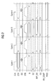
- Fig. 2 signal waveforms are shown for illustrating the method of operation of the apparatus shown in Fig. 1.
- Cycle 1 starts with the first rising edge of the timing signal CLK.
- the vector generator VECT_GEN is triggered by the rising edge of the timing signal CLK and produces the control signals CTR after a delay.
- the control signals CTR will be used by the memory MEM during cycle 2.
- Cycle 2 starts with the second rising edge of the timing signal CLK.
- the memory MEM is triggered in access mode by the rising edge of the timing signal CLK.
- the output data DO are produced by the memory MEM.
- the output data DO are sampled employing the flip-flops FF1 which are strobed by the falling edge of the delayed timing signal STB.
- the flip-flops FF1 consequently produce at their outputs Q the signal bus Q which is updated by the value of the data DO at the time when the falling edge of the delayed timing signal STB occurs.
- Cycle 3 starts with the third rising edge of the timing signal CLK.
- the flip-flops FF2 are strobed by the rising edge of the timing signal CLK and they produce data Q2 at their outputs Q.
- the vector generator VECT_GEN generates the reference values EXP_DO that are reference operands for the multi-bit comparator COMP. Afterwards the multi-bit comparator COMP generates its output signal EQ.
- Cycle 4 starts with the fourth rising edge of the timing signal CLK.
- the flip-flop FF3 functioning together with the AND gate AG as a test status generator is strobed by the rising edge of the timing signal CLK.
- the test status signal PASS is updated.
- the assumption is made that the signal PASS and the flip-flop FF3 were initialised to a high logical level prior to the cycles depicted in Fig. 2. Therefore the signal PASS can only perform a falling commutation because its function is to memorise whether at least one comparison failed.
- the signal ENAB_COMP is produced by the vector generator VECT_GEN and is used to enable the sampling of the results of the comparisons only at given cycles. In the example described here, the signal ENAB_COMP is always active. The signal ENAB_COMP would typically be activated when the memory MEM is accessed in the write mode.
Landscapes
- Tests Of Electronic Circuits (AREA)
Priority Applications (3)
| Application Number | Priority Date | Filing Date | Title |
|---|---|---|---|
| EP04290106A EP1555675B1 (de) | 2004-01-15 | 2004-01-15 | Vorrichtung zur Bestimmung der Zugriffszeit und/oder der minimalen Zykluszeit eines Speichers |
| DE602004007349T DE602004007349T2 (de) | 2004-01-15 | 2004-01-15 | Vorrichtung zur Bestimmung der Zugriffszeit und/oder der minimalen Zykluszeit eines Speichers |
| US11/036,542 US7171611B2 (en) | 2004-01-15 | 2005-01-14 | Apparatus for determining the access time and/or the minimally allowable cycle time of a memory |
Applications Claiming Priority (1)
| Application Number | Priority Date | Filing Date | Title |
|---|---|---|---|
| EP04290106A EP1555675B1 (de) | 2004-01-15 | 2004-01-15 | Vorrichtung zur Bestimmung der Zugriffszeit und/oder der minimalen Zykluszeit eines Speichers |
Publications (2)
| Publication Number | Publication Date |
|---|---|
| EP1555675A1 true EP1555675A1 (de) | 2005-07-20 |
| EP1555675B1 EP1555675B1 (de) | 2007-07-04 |
Family
ID=34610233
Family Applications (1)
| Application Number | Title | Priority Date | Filing Date |
|---|---|---|---|
| EP04290106A Expired - Lifetime EP1555675B1 (de) | 2004-01-15 | 2004-01-15 | Vorrichtung zur Bestimmung der Zugriffszeit und/oder der minimalen Zykluszeit eines Speichers |
Country Status (3)
| Country | Link |
|---|---|
| US (1) | US7171611B2 (de) |
| EP (1) | EP1555675B1 (de) |
| DE (1) | DE602004007349T2 (de) |
Families Citing this family (10)
| Publication number | Priority date | Publication date | Assignee | Title |
|---|---|---|---|---|
| US7184936B1 (en) * | 2004-07-12 | 2007-02-27 | Cisco Technology, Inc. | Timing variation measurement system and method |
| US7376001B2 (en) * | 2005-10-13 | 2008-05-20 | International Business Machines Corporation | Row circuit ring oscillator method for evaluating memory cell performance |
| US7349271B2 (en) * | 2005-10-13 | 2008-03-25 | International Business Machines Corporation | Cascaded test circuit with inter-bitline drive devices for evaluating memory cell performance |
| US7414904B2 (en) | 2006-12-12 | 2008-08-19 | International Business Machines Corporation | Method for evaluating storage cell design using a wordline timing and cell access detection circuit |
| US7409305B1 (en) | 2007-03-06 | 2008-08-05 | International Business Machines Corporation | Pulsed ring oscillator circuit for storage cell read timing evaluation |
| US7973549B2 (en) * | 2007-06-12 | 2011-07-05 | International Business Machines Corporation | Method and apparatus for calibrating internal pulses in an integrated circuit |
| US7760565B2 (en) * | 2007-07-24 | 2010-07-20 | International Business Machines Corporation | Wordline-to-bitline output timing ring oscillator circuit for evaluating storage array performance |
| US7668037B2 (en) * | 2007-11-06 | 2010-02-23 | International Business Machines Corporation | Storage array including a local clock buffer with programmable timing |
| FR3110261B1 (fr) * | 2020-05-18 | 2022-04-29 | Idemia Starchip | Procede et systeme de test d’un circuit integre |
| CN117033113B (zh) * | 2023-08-07 | 2024-03-19 | 上海奎芯集成电路设计有限公司 | 一种信号延迟的控制电路和方法 |
Citations (3)
| Publication number | Priority date | Publication date | Assignee | Title |
|---|---|---|---|---|
| US4430735A (en) * | 1981-05-26 | 1984-02-07 | Burroughs Corporation | Apparatus and technique for testing IC memories |
| US5995424A (en) * | 1997-07-16 | 1999-11-30 | Tanisys Technology, Inc. | Synchronous memory test system |
| US6266749B1 (en) * | 1997-03-14 | 2001-07-24 | Texas Instruments Incorporated | Access time measurement circuit and method |
Family Cites Families (7)
| Publication number | Priority date | Publication date | Assignee | Title |
|---|---|---|---|---|
| US6570944B2 (en) * | 2001-06-25 | 2003-05-27 | Rambus Inc. | Apparatus for data recovery in a synchronous chip-to-chip system |
| GB8717173D0 (en) | 1987-07-21 | 1987-08-26 | Logic Replacement Technology L | Time measurement apparatus |
| US5083299A (en) | 1990-07-16 | 1992-01-21 | Unisys Corporation | Tester for measuring signal propagation delay through electronic components |
| US5923676A (en) | 1996-12-20 | 1999-07-13 | Logic Vision, Inc. | Bist architecture for measurement of integrated circuit delays |
| US6370675B1 (en) * | 1998-08-18 | 2002-04-09 | Advantest Corp. | Semiconductor integrated circuit design and evaluation system using cycle base timing |
| US6567941B1 (en) * | 2000-04-12 | 2003-05-20 | Advantest Corp. | Event based test system storing pin calibration data in non-volatile memory |
| US6424583B1 (en) | 2000-11-30 | 2002-07-23 | Taiwan Semiconductor Manufacturing Co., Ltd | System and measuring access time of embedded memories |
-
2004
- 2004-01-15 EP EP04290106A patent/EP1555675B1/de not_active Expired - Lifetime
- 2004-01-15 DE DE602004007349T patent/DE602004007349T2/de not_active Expired - Lifetime
-
2005
- 2005-01-14 US US11/036,542 patent/US7171611B2/en not_active Expired - Lifetime
Patent Citations (3)
| Publication number | Priority date | Publication date | Assignee | Title |
|---|---|---|---|---|
| US4430735A (en) * | 1981-05-26 | 1984-02-07 | Burroughs Corporation | Apparatus and technique for testing IC memories |
| US6266749B1 (en) * | 1997-03-14 | 2001-07-24 | Texas Instruments Incorporated | Access time measurement circuit and method |
| US5995424A (en) * | 1997-07-16 | 1999-11-30 | Tanisys Technology, Inc. | Synchronous memory test system |
Also Published As
| Publication number | Publication date |
|---|---|
| EP1555675B1 (de) | 2007-07-04 |
| US20050204211A1 (en) | 2005-09-15 |
| DE602004007349T2 (de) | 2008-03-13 |
| DE602004007349D1 (de) | 2007-08-16 |
| US7171611B2 (en) | 2007-01-30 |
Similar Documents
| Publication | Publication Date | Title |
|---|---|---|
| US10114073B2 (en) | Integrated circuit testing | |
| US6978352B2 (en) | Memory controller emulator for controlling memory devices in a memory system | |
| US8166361B2 (en) | Integrated circuit testing module configured for set-up and hold time testing | |
| US7139957B2 (en) | Automatic self test of an integrated circuit component via AC I/O loopback | |
| US5127011A (en) | Per-pin integrated circuit test system having n-bit interface | |
| US6760873B1 (en) | Built-in self test for speed and timing margin for a source synchronous IO interface | |
| US20060253266A1 (en) | Integrated circuit test array including test module | |
| US6031382A (en) | Functional tester for integrated circuits | |
| US8001439B2 (en) | Integrated circuit testing module including signal shaping interface | |
| WO2001063311A2 (en) | Method and system for wafer and device-level testing of an integrated circuit | |
| WO2002025296A2 (en) | Method and system for wafer and device-level testing of an integrated circuit | |
| US7114114B1 (en) | Dynamically reconfigurable precision signal delay test system for automatic test equipment | |
| EP1555675B1 (de) | Vorrichtung zur Bestimmung der Zugriffszeit und/oder der minimalen Zykluszeit eines Speichers | |
| US20030005359A1 (en) | Apparatus having pattern scrambler for testing a semiconductor device and method for operating same | |
| US7080302B2 (en) | Semiconductor device and test system therefor | |
| KR100590204B1 (ko) | 온-칩 셋업/홀드 측정 회로를 포함한 집적 회로 장치 | |
| KR100514335B1 (ko) | 다중 주기 발생기를 구비하는 집적 회로 테스터 | |
| US7446551B1 (en) | Integrated circuit testing module including address generator | |
| US20040218459A1 (en) | Oscillation based access time measurement | |
| US20240418776A1 (en) | Integrated-circuit chip for retention cell testing | |
| US6381722B1 (en) | Method and apparatus for testing high speed input paths | |
| US7219270B1 (en) | Device and method for using a lessened load to measure signal skew at the output of an integrated circuit | |
| WO2022035812A1 (en) | Apparatus and method for operating source synchronous devices | |
| JP2002289000A (ja) | 半導体集積回路のテスト回路装置 |
Legal Events
| Date | Code | Title | Description |
|---|---|---|---|
| PUAI | Public reference made under article 153(3) epc to a published international application that has entered the european phase |
Free format text: ORIGINAL CODE: 0009012 |
|
| AK | Designated contracting states |
Kind code of ref document: A1 Designated state(s): AT BE BG CH CY CZ DE DK EE ES FI FR GB GR HU IE IT LI LU MC NL PT RO SE SI SK TR |
|
| AX | Request for extension of the european patent |
Extension state: AL LT LV MK |
|
| 17P | Request for examination filed |
Effective date: 20051221 |
|
| AKX | Designation fees paid |
Designated state(s): DE FR GB |
|
| GRAP | Despatch of communication of intention to grant a patent |
Free format text: ORIGINAL CODE: EPIDOSNIGR1 |
|
| GRAS | Grant fee paid |
Free format text: ORIGINAL CODE: EPIDOSNIGR3 |
|
| GRAA | (expected) grant |
Free format text: ORIGINAL CODE: 0009210 |
|
| AK | Designated contracting states |
Kind code of ref document: B1 Designated state(s): DE FR GB |
|
| REG | Reference to a national code |
Ref country code: GB Ref legal event code: FG4D |
|
| REF | Corresponds to: |
Ref document number: 602004007349 Country of ref document: DE Date of ref document: 20070816 Kind code of ref document: P |
|
| ET | Fr: translation filed | ||
| PLBE | No opposition filed within time limit |
Free format text: ORIGINAL CODE: 0009261 |
|
| STAA | Information on the status of an ep patent application or granted ep patent |
Free format text: STATUS: NO OPPOSITION FILED WITHIN TIME LIMIT |
|
| 26N | No opposition filed |
Effective date: 20080407 |
|
| GBPC | Gb: european patent ceased through non-payment of renewal fee |
Effective date: 20080115 |
|
| PG25 | Lapsed in a contracting state [announced via postgrant information from national office to epo] |
Ref country code: GB Free format text: LAPSE BECAUSE OF NON-PAYMENT OF DUE FEES Effective date: 20080115 |
|
| REG | Reference to a national code |
Ref country code: FR Ref legal event code: PLFP Year of fee payment: 13 |
|
| REG | Reference to a national code |
Ref country code: FR Ref legal event code: PLFP Year of fee payment: 14 |
|
| REG | Reference to a national code |
Ref country code: FR Ref legal event code: PLFP Year of fee payment: 15 |
|
| PGFP | Annual fee paid to national office [announced via postgrant information from national office to epo] |
Ref country code: FR Payment date: 20190123 Year of fee payment: 16 |
|
| PGFP | Annual fee paid to national office [announced via postgrant information from national office to epo] |
Ref country code: DE Payment date: 20190321 Year of fee payment: 16 |
|
| REG | Reference to a national code |
Ref country code: DE Ref legal event code: R119 Ref document number: 602004007349 Country of ref document: DE |
|
| PG25 | Lapsed in a contracting state [announced via postgrant information from national office to epo] |
Ref country code: FR Free format text: LAPSE BECAUSE OF NON-PAYMENT OF DUE FEES Effective date: 20200131 Ref country code: DE Free format text: LAPSE BECAUSE OF NON-PAYMENT OF DUE FEES Effective date: 20200801 |