EP1553155A1 - Organic electroluminescence device - Google Patents
Organic electroluminescence device Download PDFInfo
- Publication number
- EP1553155A1 EP1553155A1 EP04031026A EP04031026A EP1553155A1 EP 1553155 A1 EP1553155 A1 EP 1553155A1 EP 04031026 A EP04031026 A EP 04031026A EP 04031026 A EP04031026 A EP 04031026A EP 1553155 A1 EP1553155 A1 EP 1553155A1
- Authority
- EP
- European Patent Office
- Prior art keywords
- group
- hole blocking
- blocking layer
- organic electroluminescence
- electroluminescence device
- Prior art date
- Legal status (The legal status is an assumption and is not a legal conclusion. Google has not performed a legal analysis and makes no representation as to the accuracy of the status listed.)
- Granted
Links
- 0 *c1cc2ccccc2c2c1cccc2 Chemical compound *c1cc2ccccc2c2c1cccc2 0.000 description 1
- CBFIPOTVFMLMFQ-UHFFFAOYSA-N Ic1cc2ccccc2c2c1cccc2 Chemical compound Ic1cc2ccccc2c2c1cccc2 CBFIPOTVFMLMFQ-UHFFFAOYSA-N 0.000 description 1
Classifications
-
- C—CHEMISTRY; METALLURGY
- C09—DYES; PAINTS; POLISHES; NATURAL RESINS; ADHESIVES; COMPOSITIONS NOT OTHERWISE PROVIDED FOR; APPLICATIONS OF MATERIALS NOT OTHERWISE PROVIDED FOR
- C09K—MATERIALS FOR MISCELLANEOUS APPLICATIONS, NOT PROVIDED FOR ELSEWHERE
- C09K11/00—Luminescent materials, e.g. electroluminescent or chemiluminescent
- C09K11/06—Luminescent materials, e.g. electroluminescent or chemiluminescent containing organic luminescent materials
-
- B—PERFORMING OPERATIONS; TRANSPORTING
- B25—HAND TOOLS; PORTABLE POWER-DRIVEN TOOLS; MANIPULATORS
- B25B—TOOLS OR BENCH DEVICES NOT OTHERWISE PROVIDED FOR, FOR FASTENING, CONNECTING, DISENGAGING, OR HOLDING
- B25B1/00—Vices
- B25B1/22—Arrangements for turning or tilting vices
-
- B—PERFORMING OPERATIONS; TRANSPORTING
- B23—MACHINE TOOLS; METAL-WORKING NOT OTHERWISE PROVIDED FOR
- B23Q—DETAILS, COMPONENTS, OR ACCESSORIES FOR MACHINE TOOLS, e.g. ARRANGEMENTS FOR COPYING OR CONTROLLING; MACHINE TOOLS IN GENERAL CHARACTERISED BY THE CONSTRUCTION OF PARTICULAR DETAILS OR COMPONENTS; COMBINATIONS OR ASSOCIATIONS OF METAL-WORKING MACHINES, NOT DIRECTED TO A PARTICULAR RESULT
- B23Q3/00—Devices holding, supporting, or positioning work or tools, of a kind normally removable from the machine
- B23Q3/02—Devices holding, supporting, or positioning work or tools, of a kind normally removable from the machine for mounting on a work-table, tool-slide, or analogous part
- B23Q3/06—Work-clamping means
- B23Q3/066—Bench vices
-
- B—PERFORMING OPERATIONS; TRANSPORTING
- B25—HAND TOOLS; PORTABLE POWER-DRIVEN TOOLS; MANIPULATORS
- B25B—TOOLS OR BENCH DEVICES NOT OTHERWISE PROVIDED FOR, FOR FASTENING, CONNECTING, DISENGAGING, OR HOLDING
- B25B1/00—Vices
- B25B1/02—Vices with sliding jaws
-
- H—ELECTRICITY
- H05—ELECTRIC TECHNIQUES NOT OTHERWISE PROVIDED FOR
- H05B—ELECTRIC HEATING; ELECTRIC LIGHT SOURCES NOT OTHERWISE PROVIDED FOR; CIRCUIT ARRANGEMENTS FOR ELECTRIC LIGHT SOURCES, IN GENERAL
- H05B33/00—Electroluminescent light sources
- H05B33/12—Light sources with substantially two-dimensional [2D] radiating surfaces
- H05B33/14—Light sources with substantially two-dimensional [2D] radiating surfaces characterised by the chemical or physical composition or the arrangement of the electroluminescent material, or by the simultaneous addition of the electroluminescent material in or onto the light source
-
- H—ELECTRICITY
- H10—SEMICONDUCTOR DEVICES; ELECTRIC SOLID-STATE DEVICES NOT OTHERWISE PROVIDED FOR
- H10K—ORGANIC ELECTRIC SOLID-STATE DEVICES
- H10K50/00—Organic light-emitting devices
- H10K50/10—OLEDs or polymer light-emitting diodes [PLED]
- H10K50/18—Carrier blocking layers
-
- H—ELECTRICITY
- H10—SEMICONDUCTOR DEVICES; ELECTRIC SOLID-STATE DEVICES NOT OTHERWISE PROVIDED FOR
- H10K—ORGANIC ELECTRIC SOLID-STATE DEVICES
- H10K85/00—Organic materials used in the body or electrodes of devices covered by this subclass
- H10K85/60—Organic compounds having low molecular weight
- H10K85/615—Polycyclic condensed aromatic hydrocarbons, e.g. anthracene
- H10K85/626—Polycyclic condensed aromatic hydrocarbons, e.g. anthracene containing more than one polycyclic condensed aromatic rings, e.g. bis-anthracene
-
- H—ELECTRICITY
- H10—SEMICONDUCTOR DEVICES; ELECTRIC SOLID-STATE DEVICES NOT OTHERWISE PROVIDED FOR
- H10K—ORGANIC ELECTRIC SOLID-STATE DEVICES
- H10K85/00—Organic materials used in the body or electrodes of devices covered by this subclass
- H10K85/60—Organic compounds having low molecular weight
- H10K85/649—Aromatic compounds comprising a hetero atom
- H10K85/657—Polycyclic condensed heteroaromatic hydrocarbons
-
- C—CHEMISTRY; METALLURGY
- C09—DYES; PAINTS; POLISHES; NATURAL RESINS; ADHESIVES; COMPOSITIONS NOT OTHERWISE PROVIDED FOR; APPLICATIONS OF MATERIALS NOT OTHERWISE PROVIDED FOR
- C09K—MATERIALS FOR MISCELLANEOUS APPLICATIONS, NOT PROVIDED FOR ELSEWHERE
- C09K2211/00—Chemical nature of organic luminescent or tenebrescent compounds
- C09K2211/10—Non-macromolecular compounds
- C09K2211/1003—Carbocyclic compounds
- C09K2211/1011—Condensed systems
-
- C—CHEMISTRY; METALLURGY
- C09—DYES; PAINTS; POLISHES; NATURAL RESINS; ADHESIVES; COMPOSITIONS NOT OTHERWISE PROVIDED FOR; APPLICATIONS OF MATERIALS NOT OTHERWISE PROVIDED FOR
- C09K—MATERIALS FOR MISCELLANEOUS APPLICATIONS, NOT PROVIDED FOR ELSEWHERE
- C09K2211/00—Chemical nature of organic luminescent or tenebrescent compounds
- C09K2211/10—Non-macromolecular compounds
- C09K2211/1018—Heterocyclic compounds
- C09K2211/1025—Heterocyclic compounds characterised by ligands
- C09K2211/1029—Heterocyclic compounds characterised by ligands containing one nitrogen atom as the heteroatom
-
- H—ELECTRICITY
- H10—SEMICONDUCTOR DEVICES; ELECTRIC SOLID-STATE DEVICES NOT OTHERWISE PROVIDED FOR
- H10K—ORGANIC ELECTRIC SOLID-STATE DEVICES
- H10K2101/00—Properties of the organic materials covered by group H10K85/00
- H10K2101/10—Triplet emission
-
- H—ELECTRICITY
- H10—SEMICONDUCTOR DEVICES; ELECTRIC SOLID-STATE DEVICES NOT OTHERWISE PROVIDED FOR
- H10K—ORGANIC ELECTRIC SOLID-STATE DEVICES
- H10K50/00—Organic light-emitting devices
- H10K50/10—OLEDs or polymer light-emitting diodes [PLED]
- H10K50/11—OLEDs or polymer light-emitting diodes [PLED] characterised by the electroluminescent [EL] layers
-
- H—ELECTRICITY
- H10—SEMICONDUCTOR DEVICES; ELECTRIC SOLID-STATE DEVICES NOT OTHERWISE PROVIDED FOR
- H10K—ORGANIC ELECTRIC SOLID-STATE DEVICES
- H10K85/00—Organic materials used in the body or electrodes of devices covered by this subclass
- H10K85/30—Coordination compounds
- H10K85/321—Metal complexes comprising a group IIIA element, e.g. Tris (8-hydroxyquinoline) gallium [Gaq3]
- H10K85/324—Metal complexes comprising a group IIIA element, e.g. Tris (8-hydroxyquinoline) gallium [Gaq3] comprising aluminium, e.g. Alq3
-
- H—ELECTRICITY
- H10—SEMICONDUCTOR DEVICES; ELECTRIC SOLID-STATE DEVICES NOT OTHERWISE PROVIDED FOR
- H10K—ORGANIC ELECTRIC SOLID-STATE DEVICES
- H10K85/00—Organic materials used in the body or electrodes of devices covered by this subclass
- H10K85/30—Coordination compounds
- H10K85/341—Transition metal complexes, e.g. Ru(II)polypyridine complexes
- H10K85/342—Transition metal complexes, e.g. Ru(II)polypyridine complexes comprising iridium
-
- H—ELECTRICITY
- H10—SEMICONDUCTOR DEVICES; ELECTRIC SOLID-STATE DEVICES NOT OTHERWISE PROVIDED FOR
- H10K—ORGANIC ELECTRIC SOLID-STATE DEVICES
- H10K85/00—Organic materials used in the body or electrodes of devices covered by this subclass
- H10K85/60—Organic compounds having low molecular weight
- H10K85/631—Amine compounds having at least two aryl rest on at least one amine-nitrogen atom, e.g. triphenylamine
-
- H—ELECTRICITY
- H10—SEMICONDUCTOR DEVICES; ELECTRIC SOLID-STATE DEVICES NOT OTHERWISE PROVIDED FOR
- H10K—ORGANIC ELECTRIC SOLID-STATE DEVICES
- H10K85/00—Organic materials used in the body or electrodes of devices covered by this subclass
- H10K85/60—Organic compounds having low molecular weight
- H10K85/631—Amine compounds having at least two aryl rest on at least one amine-nitrogen atom, e.g. triphenylamine
- H10K85/633—Amine compounds having at least two aryl rest on at least one amine-nitrogen atom, e.g. triphenylamine comprising polycyclic condensed aromatic hydrocarbons as substituents on the nitrogen atom
-
- H—ELECTRICITY
- H10—SEMICONDUCTOR DEVICES; ELECTRIC SOLID-STATE DEVICES NOT OTHERWISE PROVIDED FOR
- H10K—ORGANIC ELECTRIC SOLID-STATE DEVICES
- H10K85/00—Organic materials used in the body or electrodes of devices covered by this subclass
- H10K85/60—Organic compounds having low molecular weight
- H10K85/649—Aromatic compounds comprising a hetero atom
-
- H—ELECTRICITY
- H10—SEMICONDUCTOR DEVICES; ELECTRIC SOLID-STATE DEVICES NOT OTHERWISE PROVIDED FOR
- H10K—ORGANIC ELECTRIC SOLID-STATE DEVICES
- H10K85/00—Organic materials used in the body or electrodes of devices covered by this subclass
- H10K85/60—Organic compounds having low molecular weight
- H10K85/649—Aromatic compounds comprising a hetero atom
- H10K85/654—Aromatic compounds comprising a hetero atom comprising only nitrogen as heteroatom
-
- Y—GENERAL TAGGING OF NEW TECHNOLOGICAL DEVELOPMENTS; GENERAL TAGGING OF CROSS-SECTIONAL TECHNOLOGIES SPANNING OVER SEVERAL SECTIONS OF THE IPC; TECHNICAL SUBJECTS COVERED BY FORMER USPC CROSS-REFERENCE ART COLLECTIONS [XRACs] AND DIGESTS
- Y10—TECHNICAL SUBJECTS COVERED BY FORMER USPC
- Y10S—TECHNICAL SUBJECTS COVERED BY FORMER USPC CROSS-REFERENCE ART COLLECTIONS [XRACs] AND DIGESTS
- Y10S428/00—Stock material or miscellaneous articles
- Y10S428/917—Electroluminescent
Definitions
- the present invention relates to an organic electroluminescence device.
- OLED organic light emitting diode
- An organic electroluminescence device includes an organic film which is formed between an electron injecting electrode(cathode) and a hole injecting electrode(anode), and emits light generated upon extinction after electrons and holes are paired.
- the device can be formed on a flexible transparent substrate, such as plastic, can be driven at a lower voltage (below 10V) than a plasma display panel or inorganic electroluminescence(EL) display is, has relatively low power consumption, and has a superior color sense. Further, the organic electroluminescence(EL) device can represent three colors of green, blue and red, and thus is drawing a great deal of attention as a next-generation full-color display device.
- an anode material is coated on a transparent substrate.
- Indium tin oxide(ITO) is often used as the anode material.
- a hole injecting layer(HIL) is coated thereon.
- Copper phthalocyanine(CuPC) is mainly used as the hole injecting layer at a thickness of 10 to 30nm.
- a hole transport layer(HTL) is coated.
- 4.4' -bis[N-(1-naphthyl)-N-phentylamino]-biphenyl(NPB) is deposited and coated at 30 to 60nm as the hole transport layer.
- An organic emitting layer is formed thereon. At this moment, a dopant is added thereto as needed.
- a dopant is added thereto as needed.
- tris(8-hydroxy-quinolate)aluminum(Alq3) is deposited at a thickness of 30 to 60nm as the organic emitting layer, and MQD(N-methyl quinacridone) is commonly used as the dopant.
- An electron transport layer(ETL) or electron injecting layer(EIL) are consecutively coated thereon, or an electron injecting transport layer is formed thereon.
- ETL electron transport layer
- EIL electron injecting layer
- blue, green and red light emitting devices each can be realized depending on how a light emitting layer is formed.
- the organic electroluminescence device forms excitons by the combination of holes from the hole transport layer and electrons from the electron transport layer. At this time, the excitons are protons that conduct heat without being accompanied by the movement of an electric charge in a semiconductor or insulating body.
- the excitons thus generated are dispersed a relatively long distance before extinction, and thus increases the possibility of some parts of the excitons being dispersed out of the light emitting layer.
- the excitons are dispersed and quenched by the anode.
- a hole blocking layer is used which can disperse electrons, substantially support the dispersion of excitons, and substantially prevent the dispersion of holes.
- the hole blocking layer according to the prior art is low in stability, and thus is unable to prevent the quenching of the exictons to a satisfying level.
- the present invention is directed to an organic electroluminescence device that substantially obviates one or more problems due to limitations and disadvantages of the related art.
- An object of the present invention is to provide an organic electroluminescence device which is suitable for phosphorescence and excellent in luminance and driving characteristics by comprising a hole blocking layer having an excellent stability disposed between an electron injecting electrode (cathode) and a hole injecting electrode (anode).
- the organic electroluminescence device of the present invention comprises an anode, a hole injecting layer, a hole transport layer, an emitting layer, a hole blocking layer, an electron transport layer, an electron injecting layer and a cathode, the material for the hole blocking layer is expressed by the following chemical formula 1:
- the organic electroluminescence device of the present invention comprises an anode, a hole injecting layer, a hole transport layer, an emitting layer, a hole blocking layer, an electron transport layer, an electron injecting layer and a cathode
- the material for the hole blocking layer is expressed by the following chemical formula 1: wherein A is selected from the group consisting of a substituted or non-substituted aromatic group, a hetero ring group, a substituted or non-substituted phenyl, biphenyl, pyridyl, bipyridyl, naphthyl, binaphthyl, quinoline, isoquinoline, anthracene, phenanthraene and the like.
- the substituent on the substituted aromatic group or hetero ring group is selected from the group consisting of alkyl, allyl, alkoxy, halogene, cyano and the like, or the group consisting of methyl, ethyl, isopropyl, phenyl, naphtyl, methoxy, ethoxy, fluoro, chloro, cyano and the like.
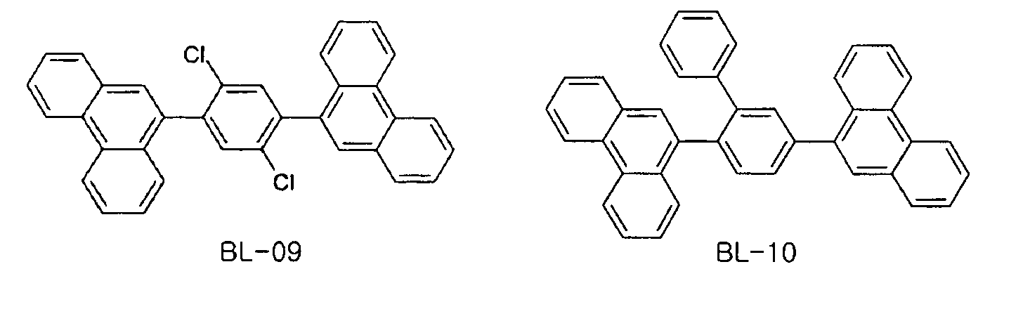
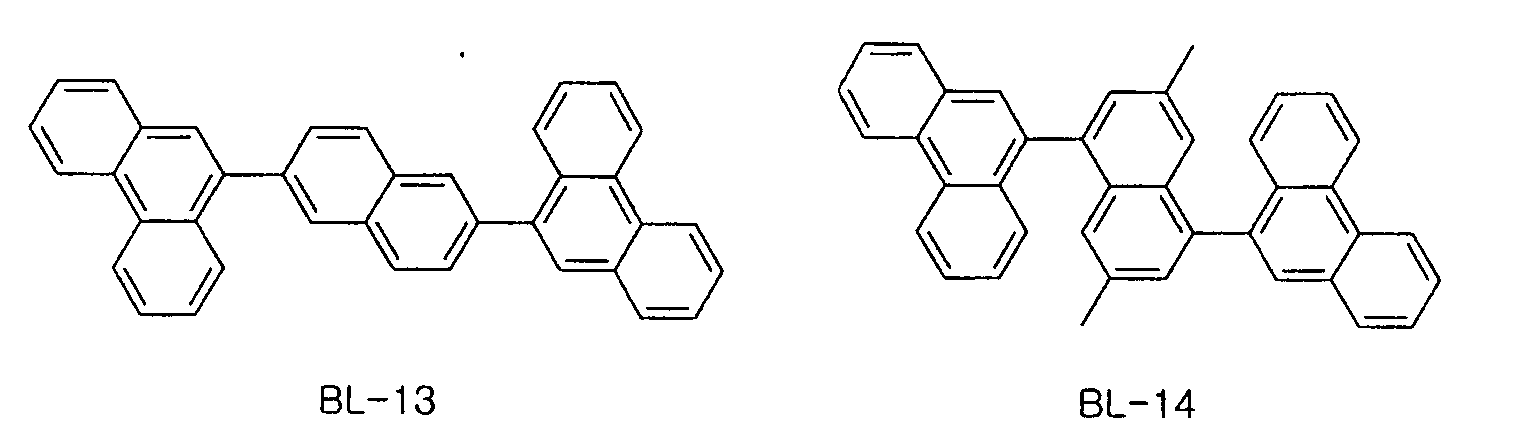
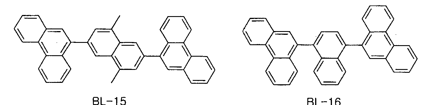
- A is expressed by one of the following chemical formulae 2: and the material for the hole blocking layer is expressed by one of the following chemical formulae 3:
- An ITO glass was patterned to have a luminescence area of 3mm X 3mm, and then washed.
- the substrate is mounted to a vacuum chamber, the base pressure was set to 1 ⁇ 10 -6 Torr, and then organic materials were deposited on the ITO in the order of HIL(600 ⁇ )/NPD(300 ⁇ )/CBP+1r(ppy) 3 (8%)(200 ⁇ )BL-01(100 ⁇ )(hole blocking layer)/Alq 3 (300 ⁇ )/LiF(5 ⁇ )/Al(1000 ⁇ ).
- the luminescence showed 2,625cd/m 2 (8.16V) at 1mA, where x and y are 0.286 and 0.628, respectively, on CIE chromaticity diagram.
- An ITO glass was patterned to have a luminescence area of 3mm ⁇ 3mm, and then washed.
- the substrate is mounted to a vacuum chamber, the base pressure was set to 1 ⁇ 10 -6 Torr, and then organic materials were deposited on the ITO in the order of HIL(600 ⁇ )/NPD(300 ⁇ )/CBP+1r(ppy) 3 (8%)(200 ⁇ )/BL-25(100 ⁇ )(hole blocking layer)/Alq 3 (300 ⁇ )/LiF(5 ⁇ )/Al(1000 ⁇ ).
- the luminescence showed 3,209cd/m 2 (8.18V) at 1mA, where x and y are 0.287 and 0.627, respectively, on CIE chromaticity diagram.
- An ITO glass was patterned to have a luminescence area of 3mm ⁇ 3mm, and then washed.
- the substrate is mounted to a vacuum chamber, the base pressure was set to 1 ⁇ 10 -6 Torr, and then organic materials were deposited on the ITO in the order of HIL(600 ⁇ )/NPD(300 ⁇ )/CBP+1r(ppy) 3 (8%)(200 ⁇ )/BAlq(100 ⁇ )(hole blocking layer)/Alq 3 (300 ⁇ )/LiF(5 ⁇ )/Al(1000 ⁇ ).
- the luminescence showed 2,893cd/m 2 (9.73V) at 1mA, where x and y are 0.318 and 0.617, respectively, on CIE chromaticity diagram.
- the structural formula of CuPC, NPB, CBP, Ir(ppy) 3 , BAlq and Alq 3 was expressed below.
- Examples 1 and 2 according to the present invention BL-1 and BL-25 were used as the hole blocking layer, respectively.
- BAlq was used as the hole blocking layer. It can be known that Examples of the present invention are superior in luminescence and driving characteristics than Comparative Example.
- the organic electroluminescence device can solve the prior art extinction problem completely and improve the luminescence and driving characteristics by forming a hole blocking layer of a material having an excellent stability, as shown in the aforementioned chemical formulae 3, between an electron injecting electrode and a hole injecting electrode.
Landscapes
- Engineering & Computer Science (AREA)
- Chemical & Material Sciences (AREA)
- Physics & Mathematics (AREA)
- Materials Engineering (AREA)
- Spectroscopy & Molecular Physics (AREA)
- Mechanical Engineering (AREA)
- Optics & Photonics (AREA)
- Organic Chemistry (AREA)
- Electroluminescent Light Sources (AREA)
Abstract

Description
- This application claims the benefit of the Korean Patent Application No. 10-2004-0000624, filed on January 6, 2004, which is hereby incorporated by reference as if fully set forth herein.
- The present invention relates to an organic electroluminescence device.
- With the recent trend of a display device' s growing in size, the need for a flat display device occupying a small space is increasing. As one of such flat display devices, the technology of organic electroluminescence device, known as an organic light emitting diode (OLED), has been developed rapidly, and a variety of sample products have been already released.
- An organic electroluminescence device includes an organic film which is formed between an electron injecting electrode(cathode) and a hole injecting electrode(anode), and emits light generated upon extinction after electrons and holes are paired. The device can be formed on a flexible transparent substrate, such as plastic, can be driven at a lower voltage (below 10V) than a plasma display panel or inorganic electroluminescence(EL) display is, has relatively low power consumption, and has a superior color sense. Further, the organic electroluminescence(EL) device can represent three colors of green, blue and red, and thus is drawing a great deal of attention as a next-generation full-color display device.
- Here, the procedure of fabricating an organic electroluminescence device will be described briefly.
- (1) Firstly, an anode material is coated on a transparent substrate. Indium tin oxide(ITO) is often used as the anode material.
- (2) A hole injecting layer(HIL) is coated thereon. Copper phthalocyanine(CuPC)is mainly used as the hole injecting layer at a thickness of 10 to 30nm.
- (3) Then, a hole transport layer(HTL) is coated. 4.4' -bis[N-(1-naphthyl)-N-phentylamino]-biphenyl(NPB) is deposited and coated at 30 to 60nm as the hole transport layer.
- (4) An organic emitting layer is formed thereon. At this moment, a dopant is added thereto as needed. In case of green luminescence, tris(8-hydroxy-quinolate)aluminum(Alq3) is deposited at a thickness of 30 to 60nm as the organic emitting layer, and MQD(N-methyl quinacridone) is commonly used as the dopant.
- (5) An electron transport layer(ETL) or electron injecting layer(EIL) are consecutively coated thereon, or an electron injecting transport layer is formed thereon. In case of green luminescence, Alq3 of the above (4) has a good electron transport capability, and thus it is often the case that no electron injecting/transport layer is used.
- (6) Next, a cathode is coated, and finally a protecting layer is coated.
- In the above structure, blue, green and red light emitting devices each can be realized depending on how a light emitting layer is formed.
- The organic electroluminescence device forms excitons by the combination of holes from the hole transport layer and electrons from the electron transport layer. At this time, the excitons are protons that conduct heat without being accompanied by the movement of an electric charge in a semiconductor or insulating body.
- The excitons thus generated are dispersed a relatively long distance before extinction, and thus increases the possibility of some parts of the excitons being dispersed out of the light emitting layer. In some cases, the excitons are dispersed and quenched by the anode. To reduce this phenomenon, a hole blocking layer is used which can disperse electrons, substantially support the dispersion of excitons, and substantially prevent the dispersion of holes.
- However, the hole blocking layer according to the prior art is low in stability, and thus is unable to prevent the quenching of the exictons to a satisfying level.
- Accordingly, the present invention is directed to an organic electroluminescence device that substantially obviates one or more problems due to limitations and disadvantages of the related art.
- An object of the present invention is to provide an organic electroluminescence device which is suitable for phosphorescence and excellent in luminance and driving characteristics by comprising a hole blocking layer having an excellent stability disposed between an electron injecting electrode (cathode) and a hole injecting electrode (anode).
- The organic electroluminescence device of the present invention comprises an anode, a hole injecting layer, a hole transport layer, an emitting layer, a hole blocking layer, an electron transport layer, an electron injecting layer and a cathode, the material for the hole blocking layer is expressed by the following chemical formula 1:

- Additional advantages, objects, and features of the invention will be set forth in part in the description which follows and in part will become apparent to those having ordinary skill in the art upon examination of the following or may be learned from practice of the invention.
- The organic electroluminescence device of the present invention comprises an anode, a hole injecting layer, a hole transport layer, an emitting layer, a hole blocking layer, an electron transport layer, an electron injecting layer and a cathode, the material for the hole blocking layer is expressed by the following chemical formula 1:wherein A is selected from the group consisting of a substituted or non-substituted aromatic group, a hetero ring group, a substituted or non-substituted phenyl, biphenyl, pyridyl, bipyridyl, naphthyl, binaphthyl, quinoline, isoquinoline, anthracene, phenanthraene and the like. The substituent on the substituted aromatic group or hetero ring group is selected from the group consisting of alkyl, allyl, alkoxy, halogene, cyano and the like, or the group consisting of methyl, ethyl, isopropyl, phenyl, naphtyl, methoxy, ethoxy, fluoro, chloro, cyano and the like.

- A is expressed by one of the following chemical formulae 2:


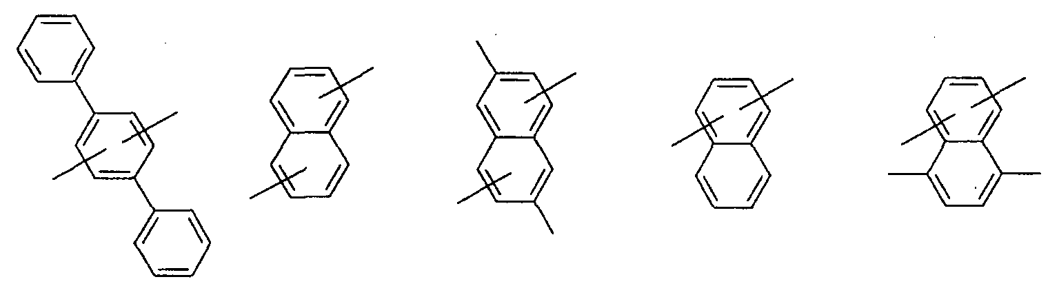

 and the material for the hole blocking layer is expressed by one of the following chemical formulae 3:

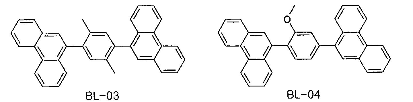

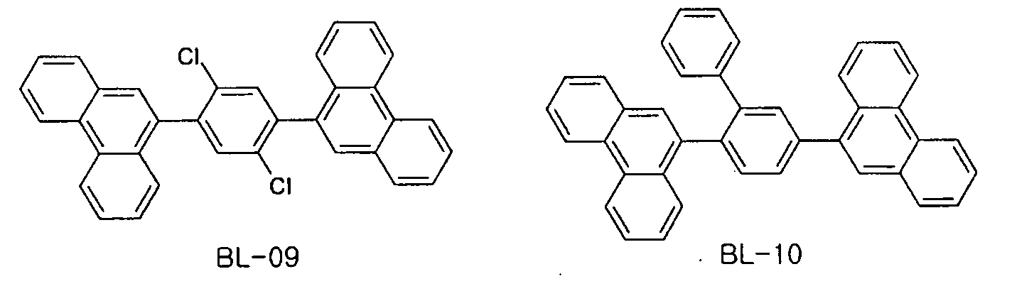
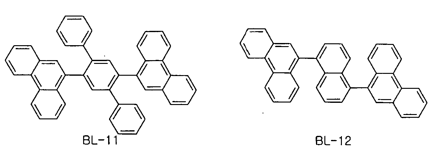
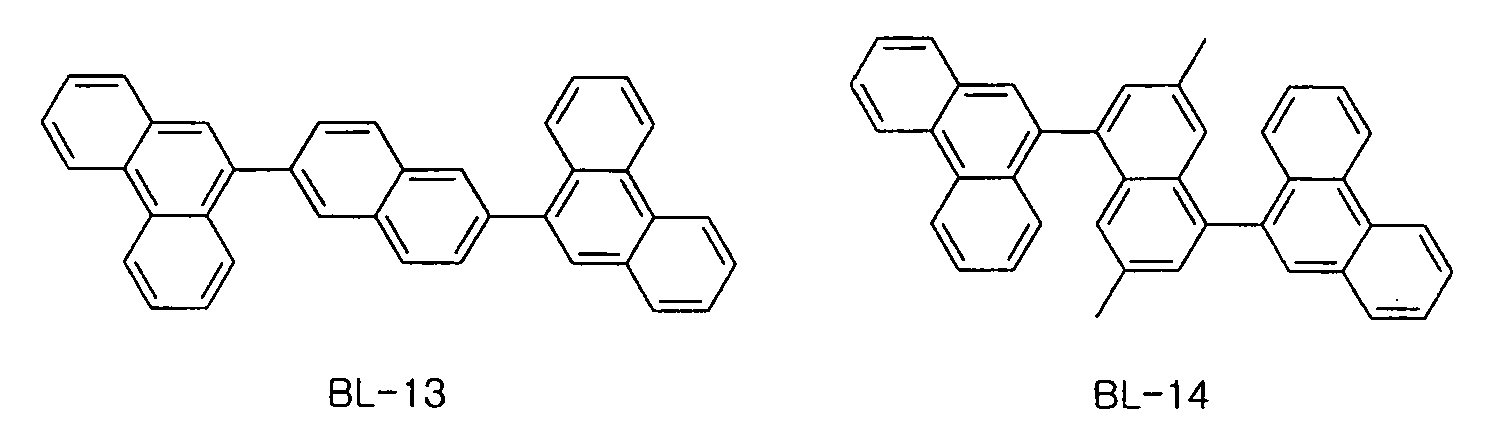


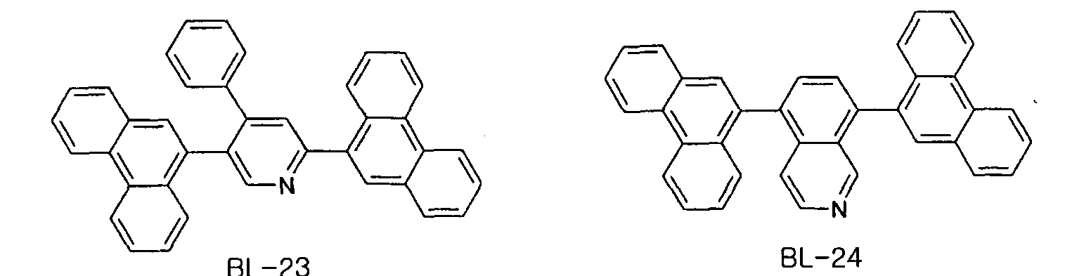

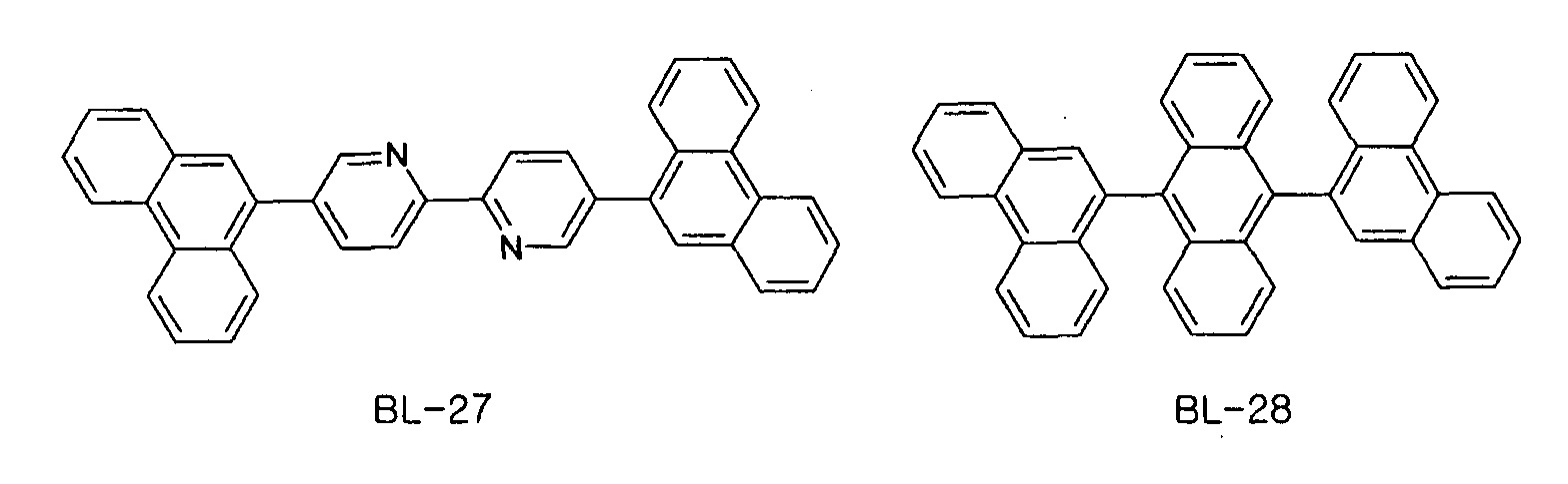
- At this time, the method of synthesis of some parts (BL-1, BL-25) of the hole blocking material as shown in formulae 3 will be described.
- 1. Synthesis of Phenanthryl Boronic AcidIn a well-dried three-neck round bottom flask, 9-bromophnanthrene (2.57g, 0.01mol) was dissolved in 100ml of anhydrous diethyl ether, and a -78°C container was disposed. To this mixture, n-BuLi (2.5M in hexane, 4mL, 0.01mol) was slowly added for 10 minutes, and stirred for 30 minutes at a room temperature. Next, a -78°C container was disposed againand trimethylborate (1.59ml, 0.014mol) was slowly added to the mixture. After addition, the mixture was stirred at the room temperature for 12 hours. After reaction, a -0°C container was disposed again, 10% hydrochloric acid was slowly added to the mixture to have a pH of 2 or 3. Next, the reaction was extracted using diethyl ether, and then the solvent was distilled under vacuum and precipitates were filtered off using petroleum ether, thereby obtaining a white solid (1.93g, 87%), i.e., phenathryl boronic acid.

- 2. Synthesis of 1,4-Diphenanthrylbenzene (BL-01)In a two-neck round bottom flask, phenanthryl boronic acid (6.3g, 0.028mol),1,4-dibromo benzene (2.68g, 0.011mol), Tetrakis(triphenylphosphine)palladium(0)(0.19g, 0.05eq), and potassium carbonate (6.21g, 0.045mol) were dissolved in toluene (80ml), THF(50mL) and water(50mL), and stirred for 24 hours in a 100°C container. After reaction, THF and toluene were removed, and the reaction was extracted using dichloromethane and water, distilled under vacuum, and purified through silica gel column chromatography. Then, the solvent was distilled under vacuum and recrystallized using dichloromethane and methanol and filtered off, thereby obtaining a product, i.e., a white solid of 1,4-diphenanthrylbenzene (3.57g, 73%).
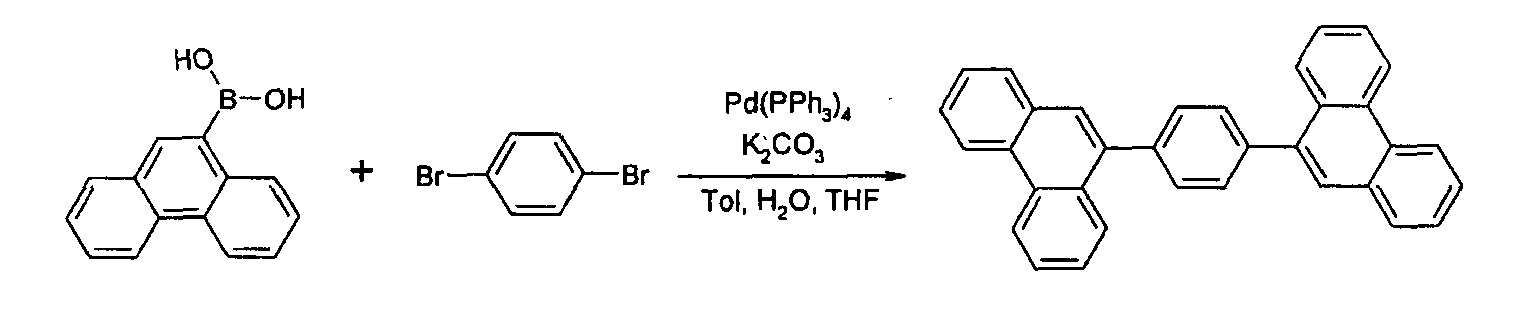
- 3. Synthesis of 1.4-diphenathrylquinoline (BL-25)In a two-neck round bottom flask, phenanthryl boronic acid (3.25g, 0.015mol),1,4-dibromo benzene (1.4g, 0.005mol), Tetrakis(triphenylphosphine)palladium(0)(0.1g, 0.05eq), and potassium carbonate (3.36g, 0.025mol) were dissolved in toluene (40ml), THF(20mL) and water(20mL), and stirred for 24 hours in a 100°C container. After reaction, THF and toluene were removed, and the reaction was extracted using dichloromethane and water, distilled under vacuum, and purified through silica gel column chromatography. Then, the solvent was distilled under vacuum and recrystallized using dichloromethane and methanol and filtered off, thereby obtaining a product, i.e., a white solid of 1,4-diphenanthrylbenzene (1.61g, 69%).

- Hereinafter, examples of the organic electroluminescence according to the present invention and the corresponding driving voltage and luminescence characteristics will be described below.
- An ITO glass was patterned to have a luminescence area of 3mm X 3mm, and then washed.
- Then, the substrate is mounted to a vacuum chamber, the base pressure was set to 1 × 10⁻⁶ Torr, and then organic materials were deposited on the ITO in the order of HIL(600Å)/NPD(300Å)/CBP+1r(ppy)3(8%)(200Å)BL-01(100Å)(hole blocking layer)/Alq3(300Å)/LiF(5Å)/Al(1000Å).
- The luminescence showed 2,625cd/m2 (8.16V) at 1mA, where x and y are 0.286 and 0.628, respectively, on CIE chromaticity diagram.
- An ITO glass was patterned to have a luminescence area of 3mm × 3mm, and then washed.
- Then, the substrate is mounted to a vacuum chamber, the base pressure was set to 1 × 10⁻⁶ Torr, and then organic materials were deposited on the ITO in the order of HIL(600Å)/NPD(300Å)/CBP+1r(ppy)3(8%)(200Å)/BL-25(100Å)(hole blocking layer)/Alq3(300Å)/LiF(5Å)/Al(1000Å).
- The luminescence showed 3,209cd/m2 (8.18V) at 1mA, where x and y are 0.287 and 0.627, respectively, on CIE chromaticity diagram.
- Comparative Example
- An ITO glass was patterned to have a luminescence area of 3mm × 3mm, and then washed.
- Then, the substrate is mounted to a vacuum chamber, the base pressure was set to 1 × 10⁻⁶ Torr, and then organic materials were deposited on the ITO in the order of HIL(600Å)/NPD(300Å)/CBP+1r(ppy)3(8%)(200Å)/BAlq(100Å)(hole blocking layer)/Alq3(300Å)/LiF(5Å)/Al(1000Å).
- The luminescence showed 2,893cd/m2 (9.73V) at 1mA, where x and y are 0.318 and 0.617, respectively, on CIE chromaticity diagram. The structural formula of CuPC, NPB, CBP, Ir(ppy)3, BAlq and Alq3 was expressed below.


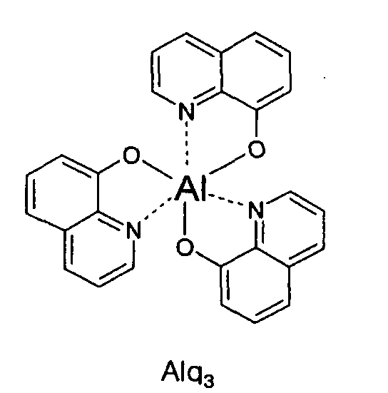
- At this time, in Examples 1 and 2 according to the present invention, BL-1 and BL-25 were used as the hole blocking layer, respectively. In the prior art illustrated by way of Comparative Example, BAlq was used as the hole blocking layer. It can be known that Examples of the present invention are superior in luminescence and driving characteristics than Comparative Example.
- Accordingly, the organic electroluminescence device according to the present invention can solve the prior art extinction problem completely and improve the luminescence and driving characteristics by forming a hole blocking layer of a material having an excellent stability, as shown in the aforementioned chemical formulae 3, between an electron injecting electrode and a hole injecting electrode.
- The forgoing embodiments are merely exemplary and are not to be construed as limiting the present invention. The present teachings can be readily applied to other types of apparatuses. The description of the present invention is intended to be illustrative, and not to limit the scope of the claims. Many alternatives, modifications, and variations will be apparent to those skilled in the art.
- The claims refer to examples of preferred embodiments of the invention. However, the invention also refers to the use of any single feature and subcombination of features which are disclosed in the claims and the description.
Claims (5)





Applications Claiming Priority (2)
| Application Number | Priority Date | Filing Date | Title |
|---|---|---|---|
| KR2004000624 | 2004-01-06 | ||
| KR1020040000624A KR100577262B1 (en) | 2004-01-06 | 2004-01-06 | Organic light emitting diode |
Publications (2)
| Publication Number | Publication Date |
|---|---|
| EP1553155A1 true EP1553155A1 (en) | 2005-07-13 |
| EP1553155B1 EP1553155B1 (en) | 2008-10-29 |
Family
ID=34588117
Family Applications (1)
| Application Number | Title | Priority Date | Filing Date |
|---|---|---|---|
| EP04031026A Expired - Lifetime EP1553155B1 (en) | 2004-01-06 | 2004-12-30 | Organic electroluminescence device |
Country Status (7)
| Country | Link |
|---|---|
| US (1) | US7709101B2 (en) |
| EP (1) | EP1553155B1 (en) |
| JP (1) | JP4209849B2 (en) |
| KR (1) | KR100577262B1 (en) |
| CN (1) | CN100456523C (en) |
| AT (1) | ATE412721T1 (en) |
| DE (1) | DE602004017413D1 (en) |
Cited By (3)
| Publication number | Priority date | Publication date | Assignee | Title |
|---|---|---|---|---|
| WO2010047707A1 (en) * | 2008-10-23 | 2010-04-29 | Universal Display Corporation | Organic light emitting device and materials for use in same |
| EP2433929A1 (en) * | 2010-09-27 | 2012-03-28 | Semiconductor Energy Laboratory Co, Ltd. | Organic Compound, Light-Emitting Element, Light-Emitting Device, Electronic Device, and Lighting Device |
| EP2553744A4 (en) * | 2010-03-31 | 2017-02-08 | Canon Kabushiki Kaisha | Organic light-emitting device |
Families Citing this family (25)
| Publication number | Priority date | Publication date | Assignee | Title |
|---|---|---|---|---|
| KR100669717B1 (en) * | 2004-07-29 | 2007-01-16 | 삼성에스디아이 주식회사 | Organic electroluminescent element |
| JP4865258B2 (en) * | 2005-06-21 | 2012-02-01 | キヤノン株式会社 | 1,8-naphthyridine compound and organic light-emitting device using the same |
| CN100341869C (en) * | 2005-11-21 | 2007-10-10 | 中国科学院长春应用化学研究所 | Phenanthrene/thiophene hybridized high-mobility organic semiconductor and application thereof |
| KR100754474B1 (en) * | 2005-12-02 | 2007-09-03 | 네오뷰코오롱 주식회사 | Anthracene-based organic light emitting compound and organic light emitting diode comprising same |
| CN100443483C (en) * | 2005-12-08 | 2008-12-17 | 中国科学院长春应用化学研究所 | Oligothiophene high-mobility organic semiconductor material terminated by fused ring unit and its application |
| KR101338253B1 (en) * | 2006-06-15 | 2013-12-09 | 삼성디스플레이 주식회사 | Cyclopentaphenanthrene-based compound and organoelectroluminescent device employing the same |
| US8211552B2 (en) | 2007-07-07 | 2012-07-03 | Idemitsu Kosan Co., Ltd. | Organic electroluminescence device |
| WO2009008205A1 (en) | 2007-07-07 | 2009-01-15 | Idemitsu Kosan Co., Ltd. | Organic electroluminescent device and material for organic electroluminescent device |
| JPWO2009008198A1 (en) | 2007-07-07 | 2010-09-02 | 出光興産株式会社 | Naphthalene derivative, material for organic EL element, and organic EL element using the same |
| US8154195B2 (en) | 2007-07-07 | 2012-04-10 | Idemitsu Kosan Co., Ltd. | Organic electroluminescence device and material for organic electroluminescence device |
| US8779655B2 (en) | 2007-07-07 | 2014-07-15 | Idemitsu Kosan Co., Ltd. | Organic electroluminescence device and material for organic electroluminescence device |
| KR101474007B1 (en) | 2007-12-10 | 2014-12-17 | 엘지디스플레이 주식회사 | Luminescent material and organic electroluminescent device including the same |
| KR100924144B1 (en) | 2008-06-05 | 2009-10-28 | 삼성모바일디스플레이주식회사 | Organic electroluminescent device and manufacturing method thereof |
| JP5279583B2 (en) | 2008-12-24 | 2013-09-04 | 出光興産株式会社 | Organic EL device |
| US8940412B2 (en) | 2008-12-26 | 2015-01-27 | Idemitsu Kosan Co., Ltd. | Material for organic electroluminescent element, and organic electroluminescent element |
| EP2372804B1 (en) | 2008-12-26 | 2014-04-02 | Idemitsu Kosan Co., Ltd. | Organic electroluminescence element and compound |
| KR20110117073A (en) | 2009-01-05 | 2011-10-26 | 이데미쓰 고산 가부시키가이샤 | Material for organic electroluminescent device and organic electroluminescent device using same |
| US8039129B2 (en) | 2009-04-06 | 2011-10-18 | Idemitsu Kosan Co., Ltd. | Organic electroluminescence device and material for organic electroluminescence device |
| US8039127B2 (en) | 2009-04-06 | 2011-10-18 | Idemitsu Kosan Co., Ltd. | Organic electroluminescence device and material for organic electroluminescence device |
| KR101256204B1 (en) * | 2009-11-02 | 2013-04-19 | (주)씨에스엘쏠라 | Organic light emitting compound and organic light emitting device comprising the same |
| JP4637271B1 (en) * | 2010-01-15 | 2011-02-23 | 富士フイルム株式会社 | Organic electroluminescence device |
| KR101799077B1 (en) | 2011-06-30 | 2017-11-20 | 삼성디스플레이 주식회사 | An organic light emitting diode and method for preparing the same |
| KR102228323B1 (en) * | 2013-11-28 | 2021-03-16 | 엘지디스플레이 주식회사 | Compound and organic light emitting device comprising the same |
| US10991915B2 (en) * | 2016-01-29 | 2021-04-27 | University Of Florida Research Foundation, Incorporated | Organic light-emitting diodes comprising grating structures and light extraction layers |
| CN116925116A (en) * | 2023-07-20 | 2023-10-24 | 烟台坤益液晶显示材料有限公司 | Preparation method of high-purity 9-phenanthreneboronic acid |
Citations (4)
| Publication number | Priority date | Publication date | Assignee | Title |
|---|---|---|---|---|
| EP1167488A1 (en) * | 1999-09-21 | 2002-01-02 | Idemitsu Kosan Company Limited | Organic electroluminescence and organic luminous medium |
| EP1253151A1 (en) * | 2001-04-25 | 2002-10-30 | Toray Industries, Inc. | Pyrromethene metal complex and light emitting device composition and light emitting devices using the same |
| US20020177009A1 (en) * | 2001-02-22 | 2002-11-28 | Koichi Suzuki | Fused polynuclear compound and organic luminescence device |
| EP1437395A2 (en) * | 2002-12-24 | 2004-07-14 | Lg Electronics Inc. | Organic electroluminescent device |
Family Cites Families (11)
| Publication number | Priority date | Publication date | Assignee | Title |
|---|---|---|---|---|
| US5077142A (en) * | 1989-04-20 | 1991-12-31 | Ricoh Company, Ltd. | Electroluminescent devices |
| US5536949A (en) * | 1992-08-28 | 1996-07-16 | Idemistu Kosan Co., Ltd. | Charge injection auxiliary material and organic electroluminescence device containing the same |
| DE69511755T2 (en) * | 1994-04-26 | 2000-01-13 | Tdk Corp | Phenylanthracene derivative and organic EL element |
| US5766779A (en) * | 1996-08-20 | 1998-06-16 | Eastman Kodak Company | Electron transporting materials for organic electroluminescent devices |
| US5645948A (en) * | 1996-08-20 | 1997-07-08 | Eastman Kodak Company | Blue organic electroluminescent devices |
| JP4783526B2 (en) | 2001-05-23 | 2011-09-28 | 本田技研工業株式会社 | Organic electroluminescence device |
| JP2003297580A (en) | 2002-04-01 | 2003-10-17 | Mitsubishi Chemicals Corp | Organic electroluminescent device |
| JP4336483B2 (en) * | 2002-09-04 | 2009-09-30 | キヤノン株式会社 | Diazafluorene compound and organic light-emitting device using the same |
| US7052351B2 (en) * | 2002-12-31 | 2006-05-30 | Eastman Kodak Company | Using hole- or electron-blocking layers in color OLEDS |
| US7651788B2 (en) * | 2003-03-05 | 2010-01-26 | Lg Display Co., Ltd. | Organic electroluminescent device |
| US9085729B2 (en) * | 2004-02-09 | 2015-07-21 | Lg Display Co., Ltd. | Blue emitters for use in organic electroluminescence devices |
-
2004
- 2004-01-06 KR KR1020040000624A patent/KR100577262B1/en not_active Expired - Lifetime
- 2004-12-30 AT AT04031026T patent/ATE412721T1/en not_active IP Right Cessation
- 2004-12-30 EP EP04031026A patent/EP1553155B1/en not_active Expired - Lifetime
- 2004-12-30 DE DE602004017413T patent/DE602004017413D1/en not_active Expired - Lifetime
-
2005
- 2005-01-05 US US11/028,734 patent/US7709101B2/en not_active Expired - Lifetime
- 2005-01-06 JP JP2005001603A patent/JP4209849B2/en not_active Expired - Lifetime
- 2005-01-06 CN CNB2005100001912A patent/CN100456523C/en not_active Expired - Lifetime
Patent Citations (4)
| Publication number | Priority date | Publication date | Assignee | Title |
|---|---|---|---|---|
| EP1167488A1 (en) * | 1999-09-21 | 2002-01-02 | Idemitsu Kosan Company Limited | Organic electroluminescence and organic luminous medium |
| US20020177009A1 (en) * | 2001-02-22 | 2002-11-28 | Koichi Suzuki | Fused polynuclear compound and organic luminescence device |
| EP1253151A1 (en) * | 2001-04-25 | 2002-10-30 | Toray Industries, Inc. | Pyrromethene metal complex and light emitting device composition and light emitting devices using the same |
| EP1437395A2 (en) * | 2002-12-24 | 2004-07-14 | Lg Electronics Inc. | Organic electroluminescent device |
Cited By (10)
| Publication number | Priority date | Publication date | Assignee | Title |
|---|---|---|---|---|
| WO2010047707A1 (en) * | 2008-10-23 | 2010-04-29 | Universal Display Corporation | Organic light emitting device and materials for use in same |
| US9112171B2 (en) | 2008-10-23 | 2015-08-18 | Universal Display Corporation | Organic light emitting device and materials for use in same |
| EP2553744A4 (en) * | 2010-03-31 | 2017-02-08 | Canon Kabushiki Kaisha | Organic light-emitting device |
| EP2433929A1 (en) * | 2010-09-27 | 2012-03-28 | Semiconductor Energy Laboratory Co, Ltd. | Organic Compound, Light-Emitting Element, Light-Emitting Device, Electronic Device, and Lighting Device |
| US8614334B2 (en) | 2010-09-27 | 2013-12-24 | Semiconductor Energy Laboratory Co., Ltd. | Organic compound, light-emitting element, light-emitting device, electronic device, and lighting device |
| US9040720B2 (en) | 2010-09-27 | 2015-05-26 | Semiconductor Energy Laboratory Co., Ltd. | Organic compound, light-emitting element, light-emitting device, electronic device, and lighting device |
| US9614164B2 (en) | 2010-09-27 | 2017-04-04 | Semiconductor Energy Laboratory Co., Ltd. | Organic compound, light-emitting element, light-emitting device, electronic device, and lighting device |
| US20170162798A1 (en) | 2010-09-27 | 2017-06-08 | Semiconductor Energy Laboratory Co., Ltd. | Organic compound, light-emitting element, light-emitting device, electronic device, and lighting device |
| US10263195B2 (en) | 2010-09-27 | 2019-04-16 | Semiconductor Energy Laboratory Co., Ltd. | Organic compound, light-emitting element, light-emitting device, electronic device, and lighting device |
| US10497880B2 (en) | 2010-09-27 | 2019-12-03 | Semiconductor Energy Laboratory Co., Ltd. | Organic compound, light-emitting element, light-emitting device, electronic device, and lighting device |
Also Published As
| Publication number | Publication date |
|---|---|
| US7709101B2 (en) | 2010-05-04 |
| US20050146268A1 (en) | 2005-07-07 |
| DE602004017413D1 (en) | 2008-12-11 |
| JP2005197262A (en) | 2005-07-21 |
| KR100577262B1 (en) | 2006-05-10 |
| ATE412721T1 (en) | 2008-11-15 |
| KR20050072247A (en) | 2005-07-11 |
| CN100456523C (en) | 2009-01-28 |
| CN1638573A (en) | 2005-07-13 |
| EP1553155B1 (en) | 2008-10-29 |
| JP4209849B2 (en) | 2009-01-14 |
Similar Documents
| Publication | Publication Date | Title |
|---|---|---|
| EP1553155B1 (en) | Organic electroluminescence device | |
| EP1317005B1 (en) | Organic electroluminescent device | |
| KR101847578B1 (en) | Fused aromatic compounds and organic light-emitting diode including the same | |
| US7449593B2 (en) | Silicon-contained anthracene compound for organic electroluminescent device | |
| CN105481811B (en) | A kind of compound and its organic electroluminescence device with spiro structure | |
| KR20110041726A (en) | Aromatic Compounds and Organic Electroluminescent Devices Using the Same | |
| KR20100109060A (en) | Novel organic electroluminescent compounds and organic electroluminescent device using the same | |
| KR101326668B1 (en) | Electron transporting-injection material and Organic electroluminescent device using the same | |
| KR20110057078A (en) | Heteroarylamine compound and organic light emitting device comprising the same | |
| KR20110041728A (en) | Aromatic Compounds and Organic Electroluminescent Devices Using the Same | |
| KR20100007639A (en) | Novel phenyl-fluorene derivatives and organic electroluminescent device comprising the same | |
| KR20100008947A (en) | Fluorenecarbazole derivative and organic electroluminescent device comprising same | |
| KR101694496B1 (en) | Dibenzothiophene derivative compound and organic electroluminescent device using the same | |
| US10396290B2 (en) | Spiro organic compounds, material comprising the same for organic electroluminescence devices, and organic electroluminescence device comprising the material | |
| EP1586616A2 (en) | Organic electroluminescence device | |
| KR20150066429A (en) | Organic Compound and Organic Light Emitting Diode Devices using the same | |
| Kim et al. | Synthesis and characterization of new blue light emitting material with tetraphenylsilyl | |
| Mi et al. | New polycyclic aromatic hydrocarbon dopants for red organic electroluminescent devices | |
| KR100948070B1 (en) | Pyrene Derivatives and Organic Electroluminescent Devices Using the Same | |
| KR20040079803A (en) | organic electroluminescence device | |
| KR100525415B1 (en) | organic electroluminescence device | |
| JP2008308449A (en) | Fused ring aromatic compound and organic light emitting device using the same | |
| Seo et al. | Efficient orange-red organic light-emitting diodes using 9, 10-bis [4-(di-4-tert-butylphenylamino) styryl] anthracene as a fluorescent orange-red emitter | |
| KR100556422B1 (en) | Blue phosphorescent organic EL device | |
| KR101561554B1 (en) | - Electron transporting-injection material and Organic electroluminescent device using the same |
Legal Events
| Date | Code | Title | Description |
|---|---|---|---|
| PUAI | Public reference made under article 153(3) epc to a published international application that has entered the european phase |
Free format text: ORIGINAL CODE: 0009012 |
|
| 17P | Request for examination filed |
Effective date: 20041230 |
|
| AK | Designated contracting states |
Kind code of ref document: A1 Designated state(s): AT BE BG CH CY CZ DE DK EE ES FI FR GB GR HU IE IS IT LI LT LU MC NL PL PT RO SE SI SK TR |
|
| AX | Request for extension of the european patent |
Extension state: AL BA HR LV MK YU |
|
| AKX | Designation fees paid |
Designated state(s): AT BE BG CH CY CZ DE DK EE ES FI FR GB GR HU IE IS IT LI LT LU MC NL PL PT RO SE SI SK TR |
|
| 17Q | First examination report despatched |
Effective date: 20051212 |
|
| GRAP | Despatch of communication of intention to grant a patent |
Free format text: ORIGINAL CODE: EPIDOSNIGR1 |
|
| RAP1 | Party data changed (applicant data changed or rights of an application transferred) |
Owner name: LG DISPLAY CO., LTD. |
|
| GRAS | Grant fee paid |
Free format text: ORIGINAL CODE: EPIDOSNIGR3 |
|
| GRAA | (expected) grant |
Free format text: ORIGINAL CODE: 0009210 |
|
| AK | Designated contracting states |
Kind code of ref document: B1 Designated state(s): AT BE BG CH CY CZ DE DK EE ES FI FR GB GR HU IE IS IT LI LT LU MC NL PL PT RO SE SI SK TR |
|
| REG | Reference to a national code |
Ref country code: GB Ref legal event code: FG4D |
|
| REG | Reference to a national code |
Ref country code: CH Ref legal event code: EP |
|
| REG | Reference to a national code |
Ref country code: IE Ref legal event code: FG4D |
|
| REF | Corresponds to: |
Ref document number: 602004017413 Country of ref document: DE Date of ref document: 20081211 Kind code of ref document: P |
|
| LTIE | Lt: invalidation of european patent or patent extension |
Effective date: 20081029 |
|
| PG25 | Lapsed in a contracting state [announced via postgrant information from national office to epo] |
Ref country code: AT Free format text: LAPSE BECAUSE OF FAILURE TO SUBMIT A TRANSLATION OF THE DESCRIPTION OR TO PAY THE FEE WITHIN THE PRESCRIBED TIME-LIMIT Effective date: 20081029 Ref country code: BG Free format text: LAPSE BECAUSE OF FAILURE TO SUBMIT A TRANSLATION OF THE DESCRIPTION OR TO PAY THE FEE WITHIN THE PRESCRIBED TIME-LIMIT Effective date: 20090129 Ref country code: LT Free format text: LAPSE BECAUSE OF FAILURE TO SUBMIT A TRANSLATION OF THE DESCRIPTION OR TO PAY THE FEE WITHIN THE PRESCRIBED TIME-LIMIT Effective date: 20081029 Ref country code: ES Free format text: LAPSE BECAUSE OF FAILURE TO SUBMIT A TRANSLATION OF THE DESCRIPTION OR TO PAY THE FEE WITHIN THE PRESCRIBED TIME-LIMIT Effective date: 20090209 |
|
| PG25 | Lapsed in a contracting state [announced via postgrant information from national office to epo] |
Ref country code: IS Free format text: LAPSE BECAUSE OF FAILURE TO SUBMIT A TRANSLATION OF THE DESCRIPTION OR TO PAY THE FEE WITHIN THE PRESCRIBED TIME-LIMIT Effective date: 20090228 Ref country code: PT Free format text: LAPSE BECAUSE OF FAILURE TO SUBMIT A TRANSLATION OF THE DESCRIPTION OR TO PAY THE FEE WITHIN THE PRESCRIBED TIME-LIMIT Effective date: 20090330 Ref country code: PL Free format text: LAPSE BECAUSE OF FAILURE TO SUBMIT A TRANSLATION OF THE DESCRIPTION OR TO PAY THE FEE WITHIN THE PRESCRIBED TIME-LIMIT Effective date: 20081029 Ref country code: FI Free format text: LAPSE BECAUSE OF FAILURE TO SUBMIT A TRANSLATION OF THE DESCRIPTION OR TO PAY THE FEE WITHIN THE PRESCRIBED TIME-LIMIT Effective date: 20081029 Ref country code: SI Free format text: LAPSE BECAUSE OF FAILURE TO SUBMIT A TRANSLATION OF THE DESCRIPTION OR TO PAY THE FEE WITHIN THE PRESCRIBED TIME-LIMIT Effective date: 20081029 |
|
| PG25 | Lapsed in a contracting state [announced via postgrant information from national office to epo] |
Ref country code: MC Free format text: LAPSE BECAUSE OF NON-PAYMENT OF DUE FEES Effective date: 20081231 Ref country code: DK Free format text: LAPSE BECAUSE OF FAILURE TO SUBMIT A TRANSLATION OF THE DESCRIPTION OR TO PAY THE FEE WITHIN THE PRESCRIBED TIME-LIMIT Effective date: 20081029 Ref country code: RO Free format text: LAPSE BECAUSE OF FAILURE TO SUBMIT A TRANSLATION OF THE DESCRIPTION OR TO PAY THE FEE WITHIN THE PRESCRIBED TIME-LIMIT Effective date: 20081029 Ref country code: EE Free format text: LAPSE BECAUSE OF FAILURE TO SUBMIT A TRANSLATION OF THE DESCRIPTION OR TO PAY THE FEE WITHIN THE PRESCRIBED TIME-LIMIT Effective date: 20081029 Ref country code: BE Free format text: LAPSE BECAUSE OF FAILURE TO SUBMIT A TRANSLATION OF THE DESCRIPTION OR TO PAY THE FEE WITHIN THE PRESCRIBED TIME-LIMIT Effective date: 20081029 |
|
| REG | Reference to a national code |
Ref country code: CH Ref legal event code: PL |
|
| PG25 | Lapsed in a contracting state [announced via postgrant information from national office to epo] |
Ref country code: SE Free format text: LAPSE BECAUSE OF FAILURE TO SUBMIT A TRANSLATION OF THE DESCRIPTION OR TO PAY THE FEE WITHIN THE PRESCRIBED TIME-LIMIT Effective date: 20090129 Ref country code: IT Free format text: LAPSE BECAUSE OF FAILURE TO SUBMIT A TRANSLATION OF THE DESCRIPTION OR TO PAY THE FEE WITHIN THE PRESCRIBED TIME-LIMIT Effective date: 20081029 Ref country code: CZ Free format text: LAPSE BECAUSE OF FAILURE TO SUBMIT A TRANSLATION OF THE DESCRIPTION OR TO PAY THE FEE WITHIN THE PRESCRIBED TIME-LIMIT Effective date: 20081029 |
|
| PLBE | No opposition filed within time limit |
Free format text: ORIGINAL CODE: 0009261 |
|
| STAA | Information on the status of an ep patent application or granted ep patent |
Free format text: STATUS: NO OPPOSITION FILED WITHIN TIME LIMIT |
|
| PG25 | Lapsed in a contracting state [announced via postgrant information from national office to epo] |
Ref country code: SK Free format text: LAPSE BECAUSE OF FAILURE TO SUBMIT A TRANSLATION OF THE DESCRIPTION OR TO PAY THE FEE WITHIN THE PRESCRIBED TIME-LIMIT Effective date: 20081029 |
|
| 26N | No opposition filed |
Effective date: 20090730 |
|
| PG25 | Lapsed in a contracting state [announced via postgrant information from national office to epo] |
Ref country code: CH Free format text: LAPSE BECAUSE OF NON-PAYMENT OF DUE FEES Effective date: 20081231 Ref country code: LI Free format text: LAPSE BECAUSE OF NON-PAYMENT OF DUE FEES Effective date: 20081231 |
|
| PG25 | Lapsed in a contracting state [announced via postgrant information from national office to epo] |
Ref country code: IE Free format text: LAPSE BECAUSE OF NON-PAYMENT OF DUE FEES Effective date: 20081230 |
|
| PG25 | Lapsed in a contracting state [announced via postgrant information from national office to epo] |
Ref country code: CY Free format text: LAPSE BECAUSE OF FAILURE TO SUBMIT A TRANSLATION OF THE DESCRIPTION OR TO PAY THE FEE WITHIN THE PRESCRIBED TIME-LIMIT Effective date: 20081029 Ref country code: HU Free format text: LAPSE BECAUSE OF FAILURE TO SUBMIT A TRANSLATION OF THE DESCRIPTION OR TO PAY THE FEE WITHIN THE PRESCRIBED TIME-LIMIT Effective date: 20090430 Ref country code: LU Free format text: LAPSE BECAUSE OF NON-PAYMENT OF DUE FEES Effective date: 20081230 |
|
| PG25 | Lapsed in a contracting state [announced via postgrant information from national office to epo] |
Ref country code: TR Free format text: LAPSE BECAUSE OF FAILURE TO SUBMIT A TRANSLATION OF THE DESCRIPTION OR TO PAY THE FEE WITHIN THE PRESCRIBED TIME-LIMIT Effective date: 20081029 |
|
| PG25 | Lapsed in a contracting state [announced via postgrant information from national office to epo] |
Ref country code: GR Free format text: LAPSE BECAUSE OF FAILURE TO SUBMIT A TRANSLATION OF THE DESCRIPTION OR TO PAY THE FEE WITHIN THE PRESCRIBED TIME-LIMIT Effective date: 20090130 |
|
| REG | Reference to a national code |
Ref country code: FR Ref legal event code: PLFP Year of fee payment: 12 |
|
| REG | Reference to a national code |
Ref country code: FR Ref legal event code: PLFP Year of fee payment: 13 |
|
| REG | Reference to a national code |
Ref country code: FR Ref legal event code: PLFP Year of fee payment: 14 |
|
| REG | Reference to a national code |
Ref country code: FR Ref legal event code: PLFP Year of fee payment: 15 |
|
| PGFP | Annual fee paid to national office [announced via postgrant information from national office to epo] |
Ref country code: NL Payment date: 20231024 Year of fee payment: 20 |
|
| PGFP | Annual fee paid to national office [announced via postgrant information from national office to epo] |
Ref country code: GB Payment date: 20231023 Year of fee payment: 20 |
|
| PGFP | Annual fee paid to national office [announced via postgrant information from national office to epo] |
Ref country code: FR Payment date: 20231024 Year of fee payment: 20 Ref country code: DE Payment date: 20231023 Year of fee payment: 20 |
|
| REG | Reference to a national code |
Ref country code: DE Ref legal event code: R071 Ref document number: 602004017413 Country of ref document: DE |
|
| PG25 | Lapsed in a contracting state [announced via postgrant information from national office to epo] |
Ref country code: GB Free format text: LAPSE BECAUSE OF EXPIRATION OF PROTECTION Effective date: 20241229 |
|
| REG | Reference to a national code |
Ref country code: GB Ref legal event code: PE20 Expiry date: 20241229 Ref country code: NL Ref legal event code: MK Effective date: 20241229 |
|
| PG25 | Lapsed in a contracting state [announced via postgrant information from national office to epo] |
Ref country code: GB Free format text: LAPSE BECAUSE OF EXPIRATION OF PROTECTION Effective date: 20241229 |