EP1548943A1 - ECL-CMOS-Pegelwandler - Google Patents
ECL-CMOS-Pegelwandler Download PDFInfo
- Publication number
- EP1548943A1 EP1548943A1 EP03360133A EP03360133A EP1548943A1 EP 1548943 A1 EP1548943 A1 EP 1548943A1 EP 03360133 A EP03360133 A EP 03360133A EP 03360133 A EP03360133 A EP 03360133A EP 1548943 A1 EP1548943 A1 EP 1548943A1
- Authority
- EP
- European Patent Office
- Prior art keywords
- cmos
- ecl
- signals
- voltage
- stage
- Prior art date
- Legal status (The legal status is an assumption and is not a legal conclusion. Google has not performed a legal analysis and makes no representation as to the accuracy of the status listed.)
- Withdrawn
Links
- 230000005669 field effect Effects 0.000 claims description 6
- 230000003287 optical effect Effects 0.000 claims description 3
- 238000006243 chemical reaction Methods 0.000 abstract description 10
- 230000001934 delay Effects 0.000 abstract description 2
- 230000003321 amplification Effects 0.000 description 3
- 238000005516 engineering process Methods 0.000 description 3
- 238000003199 nucleic acid amplification method Methods 0.000 description 3
- 230000005540 biological transmission Effects 0.000 description 2
- 238000010586 diagram Methods 0.000 description 2
- 239000004065 semiconductor Substances 0.000 description 2
- 239000000872 buffer Substances 0.000 description 1
- 230000000295 complement effect Effects 0.000 description 1
- 238000005259 measurement Methods 0.000 description 1
- 229910044991 metal oxide Inorganic materials 0.000 description 1
- 150000004706 metal oxides Chemical class 0.000 description 1
Images
Classifications
-
- H—ELECTRICITY
- H03—ELECTRONIC CIRCUITRY
- H03K—PULSE TECHNIQUE
- H03K19/00—Logic circuits, i.e. having at least two inputs acting on one output; Inverting circuits
- H03K19/0175—Coupling arrangements; Interface arrangements
- H03K19/0185—Coupling arrangements; Interface arrangements using field effect transistors only
- H03K19/018507—Interface arrangements
- H03K19/018521—Interface arrangements of complementary type, e.g. CMOS
- H03K19/018528—Interface arrangements of complementary type, e.g. CMOS with at least one differential stage
-
- H—ELECTRICITY
- H03—ELECTRONIC CIRCUITRY
- H03K—PULSE TECHNIQUE
- H03K19/00—Logic circuits, i.e. having at least two inputs acting on one output; Inverting circuits
- H03K19/0175—Coupling arrangements; Interface arrangements
- H03K19/017509—Interface arrangements
- H03K19/017518—Interface arrangements using a combination of bipolar and field effect transistors [BIFET]
- H03K19/017527—Interface arrangements using a combination of bipolar and field effect transistors [BIFET] with at least one differential stage
Definitions
- the invention relates to a converter for converting ECL (emitter coupled logic) input signals delivered from an ECL circuit part operating at a first supply voltage into CMOS (complementary metal oxide semiconductor) output signals for a CMOS circuit part operating at a second, different operating voltage.
- ECL emitter coupled logic
- CMOS complementary metal oxide semiconductor
- Logic converters are used to adjust different logic levels.
- the converter has the task of converting signals with the corresponding frequency. Such signals occur p. ex. between active components within a chip or between two chips. Theses components may be arranged close to one another or be spaced apart. For example, such components may be connected via a bus.
- the components may be integrated in network elements having a fair distance from one another.
- Signal exchanging systems in general telecommunications systems or networks, have to exchange (electrical) signals reliably and as quickly as possible.
- defined uniform transmission rates (frequencies) and defined amplitudes are used.
- Differential ECL circuits are used for data transmission due to their fast data processing and advantageous signal properties.
- the differential aspect of these signals with low potential levels leads, p. ex., to a good signal-to-noise ratio.
- An input stage receives and buffers, i.e. decouples, the ECL signals, which are supplied with a signal level swing of a few 100 mV with respect to the positive operating voltage of the ECL circuit part.
- a level shifter shifts the ECL signal level towards the CMOS threshold voltage and increases the signal level swing.
- An output stage forms a CMOS compatible output signal.
- ECL and CMOS circuit parts are often allocated to different voltage supply systems, which may vary within given tolerances.
- the supply voltage of one system may be at the upper tolerance level and the supply voltage of the other system may be at the lower tolerance level, thus further increasing the difference between the operating voltages.
- the variations of the supply voltages may vary independent from one another.
- the ECL part has an operating (supply) voltage of 3.3 V ⁇ 0.3 V and the CMOS part has an operating (supply) voltage of 1.8 V ⁇ 0.3 V.
- the converter must be able to deal with differences in supply voltage between the ECL and CMOS part of as much as 2.1 V.
- a converter for converting ECL input signals delivered from an ECL circuit part operating at a first supply voltage into CMOS output signals for a CMOS circuit part operating at a second, different operating voltage comprising an input stage for decoupling and shifting the signal level, i.e. the potential of the ECL signals, a level shifter connected to the input stage, and an output stage having the CMOS signals at its output, wherein the input stage and the level shifter are connected to the ECL operating voltage and the output stage is connected to the CMOS operating voltage.
- Such a converter works over a wide range of power supply voltages and tolerances of the operating voltages.
- the operating voltage of the ECL part may be 3.3 V ⁇ 0.3 V or 2.5 V ⁇ 0.3 V and the CMOS operating voltage may be 1.8 V ⁇ 0.3 V.
- Such a converter may be realized with few devices and therefore small circuit area.
- the number of active devices and their deviations (or size) may be kept low such that the level conversion may be performed extremely fast with propagation delays below 250 ps.
- the level shifter comprises a differential stage containing p-type field effect transistors (PFETs) or pnp bipolar transistors.
- PFETs p-type field effect transistors
- pnp bipolar differential stage works over a wide range of power supply voltages for the ECL and CMOS part.
- the differential stage may be operated with a reference voltage, which corresponds approximately to half the CMOS supply voltage.
- the voltage available for the differential stage corresponds to the ECL operating voltage minus half the CMOS supply voltage. Since the ECL supply voltage is generally larger than the CMOS supply voltage, a much larger voltage is available to the differential stage above half the CMOS supply voltage than between half the CMOS supply voltage and ground.
- a control circuit for controlling the threshold voltage of the level shifter.
- Using a control circuit allows precise control of the CMOS threshold voltage which is used as input voltage for the level shifter, thus controlling the current in the differential stage.
- the threshold voltage of the differential stage may be directly controlled by the CMOS switching threshold voltage.
- the control circuit may preferably comprise a CMOS inverter supplied with the CMOS operation voltage, two resistors for providing a mean voltage from the output signals of the level shifter, and an operational amplifier connected with the non-inverting input port and the output port to the level shifter and with the inverting input port to the CMOS inverter. Measurement of the output voltage of the level shifter allows precise control of the CMOS switching threshold voltage and results in independence from temperature or technology parameter variations.
- the measured mean voltage which corresponds to the signal level of the output signals of the level shifter, around which the output signals of the level shifter swing, is compared to the CMOS threshold voltage by the operational amplifier, the output port of which is connected to the gate of a PFET, acting as current source for the differential stage, thus controlling the current in the differential stage.
- the CMOS threshold value is easily obtained by short-circuiting the CMOS inverter.
- the input stage comprises at least one emitter follower. If two ECL signals are to be processed, in particular differential ECL signals, preferably two emitter followers are provided for decoupling the signals and reducing the potential of the ECL signals.
- the input stage may even comprise two emitter followers, if only one ECL signal is to be processed. In this case the second input port of the input stage should be supplied with a reference voltage.
- the emitter follower comprises at least one diode for reducing the ECL signal level. If a bipolar transistor with emitter and base being short-circuited is used as diode, the level of the ECL input signal may be reduced by two diode forward voltages , i.e. approximately 1.6 V. Thus, the gate voltages of the PFETs of the differential stage, which correspond to the reduced level ECL signals, are shifted into a range where variations of the operating voltages do not influence the differential amplification of the differential stage.
- the output stage comprises at least one CMOS inverter for pulse forming.
- the output stage receives signals, in case of differential ECL signals differential signals, form the level shifter. These signals are transformed into CMOS compatible output signals by the inverters in the output stage.
- CMOS inverters Preferably, for each output signal two CMOS inverters connected in series are provided.
- the inverters in the output stage are supplied with the CMOS operating voltage and are formed by p-type and n-type field effect transistors, which are identical to those used in the CMOS inverter of the control circuit.
- CMOS inverter of the control stage Supplying the CMOS inverter of the control stage, the CMOS inverters of the output stage, and the subsequent CMOS circuit part with the same operating voltage has the advantage that reliable operation of the converter is ensured even if the temperature, operating voltage and technology parameters vary. This is because the threshold value of all the CMOS inverters is the same and may be used to control the threshold voltage of the level shifter.
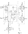
- the circuit diagram of Fig. 1 shows a converter 1 comprising an input stage 2 which is supplied with differential ECL signals ECL+, ECL- by an ECL stage not shown in Fig. 1.
- the input stage 2 comprises a first emitter follower for the signal ECL+, comprising the elements Q1, Q3, Q5 and R6, wherein Q5 and R6 form the current source of the first emitter follower.
- the input stage 2 further comprises a second emitter follower for the signal ECL-, comprising the elements Q2, Q4, Q6 and R7 , wherein Q6 and R7 form the current source of the second emitter follower.
- the input stage decouples the input signals ECL+, ECL- and shifts their potential.
- the transistors Q3, Q4 having their respective base and emitter short-circuited act as diodes for lowering the potential of the ECL input signals ECL+, ECL- by two forward diode voltages, i.e. approximately 1.6V.
- the input stage 2 is connected to the operation voltage (supply voltage) VccECL of the ECL circuit part.
- the converter 1 further comprises a level shifter 3 comprising the transistors P1 - P3, and resistors R1 - R3, wherein the transistors P1, P2 form a differential stage operating as a differential amplifier.
- the level shifter 3 is supplied with the ECL operation voltage VccECL.
- the output of the first emitter follower is connected to the gate of the p-type field effect transistor (PFET) P2 and the output of the second emitter follower is connected to the gate of the PFET P1.
- PFET p-type field effect transistor
- the gate of the PFET P3 may be supplied with a constant reference voltage, but is preferably supplied by a control circuit comprising a CMOS inverter 4 connected to an operational amplifier 5, and two resistors R4, R5.
- the level shifter 3 is dimensioned such that for a given current through the level shifter, determined by the gate voltage of PFET P3, the level of the "High" state is determined by the voltage drop at R1 and R2 or R3.
- the differential stage is designed such that the transistors P1, P2 are nearly switched off (cut-off) or on for a defined ECL input signal.
- the distribution of the current between PFETs P1, P2 depends on the exact dimensioning, wherein switching velocity, amplification and transistor size must be optimized.
- P1 or P2 In the differential stage either P1 or P2 is conducting, depending on the gate potentials. If, for example, P1 is switched on, the current flows through R1, R2, P1 and P3, resulting in a voltage drop at R1 and R2. The drain potential LS+ of P1 is then at the logic level "low” and LS- is at the logic level "high”.
- the logic levels adjusted by R1 and R2/R3 should be symmetrical to the threshold voltage of the CMOS inverters P4,PN1; P6,N3 in the output stage 6 in order to achieve fast switching.
- the threshold voltage of the CMOS inverter 4 comprising the p-type field effect transistor PDUMMY and the n-type field effect transistor NDUMMY , is used as reference input variable for the control.
- This reference input variable is directly compared by the operational amplifier 5 with the actual mean voltage of the signal level swing of the differential stage.
- the non-inverting input port of the operational amplifier is connected to the CMOS inverter 4 and the inverting input port is connected to the level shifter 3.
- the threshold voltage of the CMOS inverter 4 is generated by short circuiting the CMOS inverter 4.
- the identical resistors R4, R5 generate a mean voltage from the differential output signals LS+, LS- of the level shifter 3, which mean voltage is equal to the threshold voltage of the differential stage (P1, P2).
- the operational amplifier 5 pulls the mean voltage of the differential stage onto the threshold voltage of the CMOS inverter 4 by controlling the current through the PFET P3, which is connected to the output port of the operational amplifier 5.
- the signal levels of the output signals LS+, LS- of the level shifter 3 and hence of the differential stage (P1, P2) are always centered around the threshold voltage of the CMOS inverter 4, i.e. symmetrical to the threshold voltage.
- the CMOS inverter 4 is identical to the CMOS inverters P4, N1; P5, N2; P6, N3; P7, N4 of the output stage 6.
- the CMOS inverter 4 is supplied with the CMOS operating voltage VccCMOS , the same as the inverters P4, N1; P5, N2; P6, N3; P7, N4 of the output stage 6.
- the inverters P4, N1; P5, N2; P6, N3; P7, N4 in the output stage 6 serve for pulse forming and provide the CMOS compatible differential CMOS signals CMOS+, CMOS- for a CMOS part not shown in Fig. 1
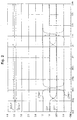
- the ECL operating (or supply) voltage VccECL is at the maximum tolerance level i.e. 3.6 V and the CMOS operating voltage is at the minimum tolerance level, i.e. 1.5 V.
- the signals ECL+, ECL- have a signal level swing of only a few hundred mV with respect to VccECL and are at a much higher signal level than the signals LS+, LS- and CMOS+, CMOS-.
- the signal level of the signals ECL+, ECL- is shifted towards the CMOS threshold voltage, which may be seen by signals LS+, LS-.
- LS+ and LS- are not only shifted towards the CMOS threshold voltage, but their signal level swing is also increased.
- the signals LS+ and LS - respectively are then converted into the signals CMOS+, CMOS -.
- the propagation delay in this case is approximately 170 ps for conversion of the ECL+ signal into the CMOS+ signal and for conversion of the ECL- signal into the CMOS- signal.
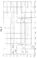
- Fig. 3 shows the signal levels for VccECL being at the minimum tolerance level i.e. 3.0 V and the CMOS operating voltage being at the maximum tolerance level, i.e. 2.1 V.
- the signal level of the signals LS+, LS- is higher because the CMOS threshold voltage is higher and the signals LS+, LS- are centered on the CMOS threshold voltage.
- the propagation delay in this case is approximately 240 ps for conversion of the ECL+ signal into the CMOS+ signal and for conversion of the ECL- signal into the CMOS- signal.
Landscapes
- Engineering & Computer Science (AREA)
- Computer Hardware Design (AREA)
- Physics & Mathematics (AREA)
- Computing Systems (AREA)
- General Engineering & Computer Science (AREA)
- Mathematical Physics (AREA)
- Logic Circuits (AREA)
Priority Applications (1)
| Application Number | Priority Date | Filing Date | Title |
|---|---|---|---|
| EP03360133A EP1548943A1 (de) | 2003-11-28 | 2003-11-28 | ECL-CMOS-Pegelwandler |
Applications Claiming Priority (1)
| Application Number | Priority Date | Filing Date | Title |
|---|---|---|---|
| EP03360133A EP1548943A1 (de) | 2003-11-28 | 2003-11-28 | ECL-CMOS-Pegelwandler |
Publications (1)
| Publication Number | Publication Date |
|---|---|
| EP1548943A1 true EP1548943A1 (de) | 2005-06-29 |
Family
ID=34530853
Family Applications (1)
| Application Number | Title | Priority Date | Filing Date |
|---|---|---|---|
| EP03360133A Withdrawn EP1548943A1 (de) | 2003-11-28 | 2003-11-28 | ECL-CMOS-Pegelwandler |
Country Status (1)
| Country | Link |
|---|---|
| EP (1) | EP1548943A1 (de) |
Cited By (1)
| Publication number | Priority date | Publication date | Assignee | Title |
|---|---|---|---|---|
| DE102005007579A1 (de) * | 2005-02-18 | 2006-08-24 | Infineon Technologies Ag | Empfängerschaltung |
Citations (4)
| Publication number | Priority date | Publication date | Assignee | Title |
|---|---|---|---|---|
| US4453095A (en) * | 1982-07-16 | 1984-06-05 | Motorola Inc. | ECL MOS Buffer circuits |
| JPS62123825A (ja) * | 1985-11-25 | 1987-06-05 | Hitachi Ltd | 論理レベル変換回路 |
| US5434518A (en) * | 1992-10-02 | 1995-07-18 | National Semiconductor Corporation | ECL-to-BICOMS/CMOS translator |
| EP1248371A1 (de) * | 2001-04-06 | 2002-10-09 | STMicroelectronics S.r.l. | Wandler zur Pegelwandlung von differentiellen Signalen |
-
2003
- 2003-11-28 EP EP03360133A patent/EP1548943A1/de not_active Withdrawn
Patent Citations (4)
| Publication number | Priority date | Publication date | Assignee | Title |
|---|---|---|---|---|
| US4453095A (en) * | 1982-07-16 | 1984-06-05 | Motorola Inc. | ECL MOS Buffer circuits |
| JPS62123825A (ja) * | 1985-11-25 | 1987-06-05 | Hitachi Ltd | 論理レベル変換回路 |
| US5434518A (en) * | 1992-10-02 | 1995-07-18 | National Semiconductor Corporation | ECL-to-BICOMS/CMOS translator |
| EP1248371A1 (de) * | 2001-04-06 | 2002-10-09 | STMicroelectronics S.r.l. | Wandler zur Pegelwandlung von differentiellen Signalen |
Non-Patent Citations (2)
| Title |
|---|
| HIRSCHAUER P: "LA TECHNOLOGIE BICMOS: LES AVANTAGES DU BIPOLAIRE ET DU CMOS SANS LEURS INCONVENIENTS", TOUTE L'ELECTRONIQUE, SOCIETE DES EDITIONS RADIO. PARIS, FR, no. 544, 1 May 1989 (1989-05-01), pages 22 - 26, XP000112304 * |
| PATENT ABSTRACTS OF JAPAN vol. 0113, no. 43 (E - 555) 10 November 1987 (1987-11-10) * |
Cited By (2)
| Publication number | Priority date | Publication date | Assignee | Title |
|---|---|---|---|---|
| DE102005007579A1 (de) * | 2005-02-18 | 2006-08-24 | Infineon Technologies Ag | Empfängerschaltung |
| US7372331B2 (en) | 2005-02-18 | 2008-05-13 | Infineon Technologies Ag | Receiver circuit |
Similar Documents
| Publication | Publication Date | Title |
|---|---|---|
| US5122690A (en) | Interface circuits including driver circuits with switching noise reduction | |
| JP2640443B2 (ja) | Cmos技術による光源の高速駆動用回路 | |
| US6294932B1 (en) | Input circuit, output circuit, input-output circuit and method of processing input signals | |
| JPH02290327A (ja) | デジタル・インタフェース回路、デジタル入力回路及びデジタル変換回路 | |
| US10079603B1 (en) | Configurable, multi-functional driver circuit | |
| US7154981B2 (en) | Termination circuit | |
| IE902799A1 (en) | High speed cmos differential interface circuits | |
| US5214317A (en) | CMOS to ECL translator with incorporated latch | |
| US20220224336A1 (en) | Digital logic compatible inputs in compound semiconductor circuits | |
| US7961013B2 (en) | Inverter circuit | |
| US5699002A (en) | Flip-flop circuit, and shift register circuit, serial-parallel converter and parallel-serial converter using the same | |
| JPH0379121A (ja) | 半導体集積回路装置 | |
| US6759905B2 (en) | Analog input circuit with common mode compatibility to both supply nodes | |
| EP1548943A1 (de) | ECL-CMOS-Pegelwandler | |
| EP1376867A1 (de) | Differenzverstärker zur schneller CMOS-ECL-Konversion | |
| US11863360B2 (en) | Methods and apparatus to reduce variations for on-off keying transmissions | |
| EP0803947A2 (de) | Hochgeschwindigkeitsschaltung in cmos Technologie für optische Quellen | |
| US6803820B1 (en) | Apparatus and method for reducing common-mode current in differential link | |
| US7138822B2 (en) | Integrated circuit and method of improving signal integrity | |
| JPH077407A (ja) | 半導体集積回路装置 | |
| US12283958B2 (en) | Driver circuit for low voltage differential signaling, LVDS, line driver arrangement for LVDS and method for operating an LVDS driver circuit | |
| US6956400B2 (en) | Converter from ECL to CMOS and network element for transmitting signals | |
| USRE44134E1 (en) | Universal input apparatus | |
| US5633602A (en) | Low voltage CMOS to low voltage PECL converter | |
| EP1612941A1 (de) | Leistungspegelkonverterschaltung |
Legal Events
| Date | Code | Title | Description |
|---|---|---|---|
| PUAI | Public reference made under article 153(3) epc to a published international application that has entered the european phase |
Free format text: ORIGINAL CODE: 0009012 |
|
| AK | Designated contracting states |
Kind code of ref document: A1 Designated state(s): AT BE BG CH CY CZ DE DK EE ES FI FR GB GR HU IE IT LI LU MC NL PT RO SE SI SK TR |
|
| AX | Request for extension of the european patent |
Extension state: AL LT LV MK |
|
| AKX | Designation fees paid | ||
| STAA | Information on the status of an ep patent application or granted ep patent |
Free format text: STATUS: THE APPLICATION IS DEEMED TO BE WITHDRAWN |
|
| 18D | Application deemed to be withdrawn |
Effective date: 20051230 |
|
| REG | Reference to a national code |
Ref country code: DE Ref legal event code: 8566 |