EP1548904B1 - Silicon nitride thin film for optical device and fabrication method thereof - Google Patents
Silicon nitride thin film for optical device and fabrication method thereof Download PDFInfo
- Publication number
- EP1548904B1 EP1548904B1 EP04018719A EP04018719A EP1548904B1 EP 1548904 B1 EP1548904 B1 EP 1548904B1 EP 04018719 A EP04018719 A EP 04018719A EP 04018719 A EP04018719 A EP 04018719A EP 1548904 B1 EP1548904 B1 EP 1548904B1
- Authority
- EP
- European Patent Office
- Prior art keywords
- silicon nitride
- thin film
- rare earth
- earth elements
- amorphous silicon
- Prior art date
- Legal status (The legal status is an assumption and is not a legal conclusion. Google has not performed a legal analysis and makes no representation as to the accuracy of the status listed.)
- Expired - Lifetime
Links
- 239000010409 thin film Substances 0.000 title claims description 52
- 229910052581 Si3N4 Inorganic materials 0.000 title claims description 50
- HQVNEWCFYHHQES-UHFFFAOYSA-N silicon nitride Chemical compound N12[Si]34N5[Si]62N3[Si]51N64 HQVNEWCFYHHQES-UHFFFAOYSA-N 0.000 title claims description 50
- 230000003287 optical effect Effects 0.000 title claims description 28
- 238000000034 method Methods 0.000 title claims description 25
- 238000004519 manufacturing process Methods 0.000 title 1
- 229910021417 amorphous silicon Inorganic materials 0.000 claims description 37
- 229910052761 rare earth metal Inorganic materials 0.000 claims description 35
- 150000003376 silicon Chemical class 0.000 claims description 32
- 229910052691 Erbium Inorganic materials 0.000 claims description 24
- UYAHIZSMUZPPFV-UHFFFAOYSA-N erbium Chemical compound [Er] UYAHIZSMUZPPFV-UHFFFAOYSA-N 0.000 claims description 24
- 239000002096 quantum dot Substances 0.000 claims description 8
- 238000007669 thermal treatment Methods 0.000 claims description 8
- 238000000623 plasma-assisted chemical vapour deposition Methods 0.000 claims description 6
- 239000002994 raw material Substances 0.000 claims description 5
- 238000000151 deposition Methods 0.000 claims description 3
- 229910052751 metal Inorganic materials 0.000 claims description 3
- 239000002184 metal Substances 0.000 claims description 3
- 229910052693 Europium Inorganic materials 0.000 claims description 2
- 229910052688 Gadolinium Inorganic materials 0.000 claims description 2
- 229910052771 Terbium Inorganic materials 0.000 claims description 2
- 229910052769 Ytterbium Inorganic materials 0.000 claims description 2
- OGPBJKLSAFTDLK-UHFFFAOYSA-N europium atom Chemical compound [Eu] OGPBJKLSAFTDLK-UHFFFAOYSA-N 0.000 claims description 2
- UIWYJDYFSGRHKR-UHFFFAOYSA-N gadolinium atom Chemical compound [Gd] UIWYJDYFSGRHKR-UHFFFAOYSA-N 0.000 claims description 2
- GZCRRIHWUXGPOV-UHFFFAOYSA-N terbium atom Chemical compound [Tb] GZCRRIHWUXGPOV-UHFFFAOYSA-N 0.000 claims description 2
- NAWDYIZEMPQZHO-UHFFFAOYSA-N ytterbium Chemical compound [Yb] NAWDYIZEMPQZHO-UHFFFAOYSA-N 0.000 claims description 2
- 230000008021 deposition Effects 0.000 claims 2
- 238000004544 sputter deposition Methods 0.000 claims 2
- 238000005468 ion implantation Methods 0.000 claims 1
- 230000005284 excitation Effects 0.000 description 11
- 229910021419 crystalline silicon Inorganic materials 0.000 description 10
- VYPSYNLAJGMNEJ-UHFFFAOYSA-N Silicium dioxide Chemical compound O=[Si]=O VYPSYNLAJGMNEJ-UHFFFAOYSA-N 0.000 description 7
- 239000007789 gas Substances 0.000 description 7
- 230000006798 recombination Effects 0.000 description 5
- 238000005215 recombination Methods 0.000 description 5
- 150000004767 nitrides Chemical class 0.000 description 4
- 238000005424 photoluminescence Methods 0.000 description 3
- 229910052814 silicon oxide Inorganic materials 0.000 description 3
- BLRPTPMANUNPDV-UHFFFAOYSA-N Silane Chemical compound [SiH4] BLRPTPMANUNPDV-UHFFFAOYSA-N 0.000 description 2
- XUIMIQQOPSSXEZ-UHFFFAOYSA-N Silicon Chemical compound [Si] XUIMIQQOPSSXEZ-UHFFFAOYSA-N 0.000 description 2
- 230000000630 rising effect Effects 0.000 description 2
- 229910000077 silane Inorganic materials 0.000 description 2
- 229910052710 silicon Inorganic materials 0.000 description 2
- 239000010703 silicon Substances 0.000 description 2
- 239000000377 silicon dioxide Substances 0.000 description 2
- QGZKDVFQNNGYKY-UHFFFAOYSA-N Ammonia Chemical compound N QGZKDVFQNNGYKY-UHFFFAOYSA-N 0.000 description 1
- IJGRMHOSHXDMSA-UHFFFAOYSA-N Atomic nitrogen Chemical compound N#N IJGRMHOSHXDMSA-UHFFFAOYSA-N 0.000 description 1
- XGYVOSQHOAYKBD-UHFFFAOYSA-N COC([O-])C.[Er+3].COC([O-])C.COC([O-])C Chemical compound COC([O-])C.[Er+3].COC([O-])C.COC([O-])C XGYVOSQHOAYKBD-UHFFFAOYSA-N 0.000 description 1
- QVGXLLKOCUKJST-UHFFFAOYSA-N atomic oxygen Chemical compound [O] QVGXLLKOCUKJST-UHFFFAOYSA-N 0.000 description 1
- ZVNGWTZZRANJAO-UHFFFAOYSA-N bis(trimethylsilyl)azanide;erbium(3+) Chemical compound [Er+3].C[Si](C)(C)[N-][Si](C)(C)C.C[Si](C)(C)[N-][Si](C)(C)C.C[Si](C)(C)[N-][Si](C)(C)C ZVNGWTZZRANJAO-UHFFFAOYSA-N 0.000 description 1
- 229910001873 dinitrogen Inorganic materials 0.000 description 1
- 150000002500 ions Chemical class 0.000 description 1
- 239000001301 oxygen Substances 0.000 description 1
- 229910052760 oxygen Inorganic materials 0.000 description 1
- 238000011160 research Methods 0.000 description 1
- 239000004065 semiconductor Substances 0.000 description 1
- 239000000758 substrate Substances 0.000 description 1
Images
Classifications
-
- H—ELECTRICITY
- H01—ELECTRIC ELEMENTS
- H01S—DEVICES USING THE PROCESS OF LIGHT AMPLIFICATION BY STIMULATED EMISSION OF RADIATION [LASER] TO AMPLIFY OR GENERATE LIGHT; DEVICES USING STIMULATED EMISSION OF ELECTROMAGNETIC RADIATION IN WAVE RANGES OTHER THAN OPTICAL
- H01S3/00—Lasers, i.e. devices using stimulated emission of electromagnetic radiation in the infrared, visible or ultraviolet wave range
- H01S3/05—Construction or shape of optical resonators; Accommodation of active medium therein; Shape of active medium
- H01S3/06—Construction or shape of active medium
- H01S3/063—Waveguide lasers, i.e. whereby the dimensions of the waveguide are of the order of the light wavelength
- H01S3/0632—Thin film lasers in which light propagates in the plane of the thin film
-
- H—ELECTRICITY
- H01—ELECTRIC ELEMENTS
- H01L—SEMICONDUCTOR DEVICES NOT COVERED BY CLASS H10
- H01L29/00—Semiconductor devices specially adapted for rectifying, amplifying, oscillating or switching and having potential barriers; Capacitors or resistors having potential barriers, e.g. a PN-junction depletion layer or carrier concentration layer; Details of semiconductor bodies or of electrodes thereof ; Multistep manufacturing processes therefor
- H01L29/02—Semiconductor bodies ; Multistep manufacturing processes therefor
- H01L29/06—Semiconductor bodies ; Multistep manufacturing processes therefor characterised by their shape; characterised by the shapes, relative sizes, or dispositions of the semiconductor regions ; characterised by the concentration or distribution of impurities within semiconductor regions
-
- B—PERFORMING OPERATIONS; TRANSPORTING
- B82—NANOTECHNOLOGY
- B82Y—SPECIFIC USES OR APPLICATIONS OF NANOSTRUCTURES; MEASUREMENT OR ANALYSIS OF NANOSTRUCTURES; MANUFACTURE OR TREATMENT OF NANOSTRUCTURES
- B82Y20/00—Nanooptics, e.g. quantum optics or photonic crystals
-
- H—ELECTRICITY
- H01—ELECTRIC ELEMENTS
- H01L—SEMICONDUCTOR DEVICES NOT COVERED BY CLASS H10
- H01L29/00—Semiconductor devices specially adapted for rectifying, amplifying, oscillating or switching and having potential barriers; Capacitors or resistors having potential barriers, e.g. a PN-junction depletion layer or carrier concentration layer; Details of semiconductor bodies or of electrodes thereof ; Multistep manufacturing processes therefor
- H01L29/02—Semiconductor bodies ; Multistep manufacturing processes therefor
- H01L29/12—Semiconductor bodies ; Multistep manufacturing processes therefor characterised by the materials of which they are formed
- H01L29/15—Structures with periodic or quasi periodic potential variation, e.g. multiple quantum wells, superlattices
-
- B—PERFORMING OPERATIONS; TRANSPORTING
- B82—NANOTECHNOLOGY
- B82Y—SPECIFIC USES OR APPLICATIONS OF NANOSTRUCTURES; MEASUREMENT OR ANALYSIS OF NANOSTRUCTURES; MANUFACTURE OR TREATMENT OF NANOSTRUCTURES
- B82Y10/00—Nanotechnology for information processing, storage or transmission, e.g. quantum computing or single electron logic
-
- H—ELECTRICITY
- H01—ELECTRIC ELEMENTS
- H01S—DEVICES USING THE PROCESS OF LIGHT AMPLIFICATION BY STIMULATED EMISSION OF RADIATION [LASER] TO AMPLIFY OR GENERATE LIGHT; DEVICES USING STIMULATED EMISSION OF ELECTROMAGNETIC RADIATION IN WAVE RANGES OTHER THAN OPTICAL
- H01S3/00—Lasers, i.e. devices using stimulated emission of electromagnetic radiation in the infrared, visible or ultraviolet wave range
- H01S3/14—Lasers, i.e. devices using stimulated emission of electromagnetic radiation in the infrared, visible or ultraviolet wave range characterised by the material used as the active medium
- H01S3/16—Solid materials
- H01S3/1601—Solid materials characterised by an active (lasing) ion
- H01S3/1603—Solid materials characterised by an active (lasing) ion rare earth
-
- H—ELECTRICITY
- H01—ELECTRIC ELEMENTS
- H01S—DEVICES USING THE PROCESS OF LIGHT AMPLIFICATION BY STIMULATED EMISSION OF RADIATION [LASER] TO AMPLIFY OR GENERATE LIGHT; DEVICES USING STIMULATED EMISSION OF ELECTROMAGNETIC RADIATION IN WAVE RANGES OTHER THAN OPTICAL
- H01S3/00—Lasers, i.e. devices using stimulated emission of electromagnetic radiation in the infrared, visible or ultraviolet wave range
- H01S3/14—Lasers, i.e. devices using stimulated emission of electromagnetic radiation in the infrared, visible or ultraviolet wave range characterised by the material used as the active medium
- H01S3/16—Solid materials
- H01S3/163—Solid materials characterised by a crystal matrix
-
- H—ELECTRICITY
- H01—ELECTRIC ELEMENTS
- H01S—DEVICES USING THE PROCESS OF LIGHT AMPLIFICATION BY STIMULATED EMISSION OF RADIATION [LASER] TO AMPLIFY OR GENERATE LIGHT; DEVICES USING STIMULATED EMISSION OF ELECTROMAGNETIC RADIATION IN WAVE RANGES OTHER THAN OPTICAL
- H01S3/00—Lasers, i.e. devices using stimulated emission of electromagnetic radiation in the infrared, visible or ultraviolet wave range
- H01S3/14—Lasers, i.e. devices using stimulated emission of electromagnetic radiation in the infrared, visible or ultraviolet wave range characterised by the material used as the active medium
- H01S3/16—Solid materials
- H01S3/1685—Ceramics
-
- H—ELECTRICITY
- H01—ELECTRIC ELEMENTS
- H01S—DEVICES USING THE PROCESS OF LIGHT AMPLIFICATION BY STIMULATED EMISSION OF RADIATION [LASER] TO AMPLIFY OR GENERATE LIGHT; DEVICES USING STIMULATED EMISSION OF ELECTROMAGNETIC RADIATION IN WAVE RANGES OTHER THAN OPTICAL
- H01S3/00—Lasers, i.e. devices using stimulated emission of electromagnetic radiation in the infrared, visible or ultraviolet wave range
- H01S3/14—Lasers, i.e. devices using stimulated emission of electromagnetic radiation in the infrared, visible or ultraviolet wave range characterised by the material used as the active medium
- H01S3/16—Solid materials
- H01S3/1691—Solid materials characterised by additives / sensitisers / promoters as further dopants
Definitions
- the present invention relates to a silicon nitride thin film and method for fabricating the same, and more particularly, to a silicon nitride thin film and method for fabricating the same, which comprises rare earth elements and amorphous silicon quantum dots in the silicon nitride thin film to enhance excitation efficiency of the rare earth element, so that it may be effectively applied to an optical device.
- silica based thin films doped with rare earth elements are widely used to fabricate a waveguide optical amplifier.
- an excitation cross sectional area of the rare earth element is very small to a degree of about 1x10 -21 cm -2 , so that the optical efficiency is significantly low in this case.
- excitation efficiency of the rare earth elements becomes higher, because the recombination efficiency of electrons and holes within the nano-dots is very high to thereby effectively excite rare earth elements. For this reason, development and researches for the silicon oxide thin film in which crystalline silicon nano-dots are comprised are conducted in recent years.
- US Patent Application US 2002/0153522 discloses a silicon nitride thin film for an optical device comprising amorphous silicon quantum dots.
- the optical efficiency is not sufficient for application of a light-emitting device so as to have high efficiency, and an oxide based thin film is used, so that an operating voltage of the device is still high.
- the present invention is directed to a silicon nitride thin film wherein rare earth elements are excited by amorphous silicon quantum dots, which are superior to crystalline silicon nano-dots in terms of luminous efficiency to thereby enhance luminous efficiency of rare earth elements.
- the present invention is also directed to a method for fabricating silicon nitride thin film having a relatively small energy gap instead of silicon oxide to enhance operation characteristics of a device when the device is fabricated.
- One aspect of the present invention is to provide a silicon nitride thin film for an optical device, wherein amorphous silicon quantum dots and rare earth elements are comprised in the silicon nitride thin film, and rare earth elements are excited by the amorphous silicon quantum dots to emit light.
- Another aspect of the present invention is to provide a method for fabricating a silicon nitride thin film for an optical device, which comprises steps of growing silicon nitride in which amorphous silicon quantum dots are comprised, and doping rare earth elements within the silicon nitride thin film, wherein rare earth elements are excited by the amorphous silicon quantum dots to emit light.
- Still another aspect of the present invention is to provide a method for fabricating a silicon nitride thin film for an optical device, which comprises doping rare earth elements within the silicon nitride thin film while growing silicon nitride in which amorphous silicon quantum dots are comprised, wherein rare earth elements are excited by the amorphous silicon quantum dots to emit light.
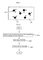
- FIG. 1 is a conceptual view of a silicon nitride thin film for an optical device in accordance with an embodiment of the present invention.
- FIG. 2 is a flow chart for explaining a method for fabricating a silicon nitride thin film for an optical device in accordance with an embodiment of the present invention.
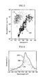
- FIG. 3 is a graph for showing luminous efficiencies of crystalline silicon nano-dots and amorphous silicon quantum dots.
- FIG. 4 is a graph for showing luminous characteristic of erbium doped within a silicon nitride thin film for an optical device, and luminous characteristic of erbium doped within crystalline silicon in accordance with an embodiment of the present invention.
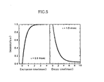
- FIG. 5 is a graph for showing decay and rise phenomena of photoluminescence measured to compute an excitation cross sectional area of erbium in the silicon nitride thin film for the optical device of FIG. 4 in terms of time.
- FIG. 1 is a conceptual view of a silicon nitride thin film for an optical device in accordance with an embodiment of the present invention.
- the silicon nitride thin film for the optical device 500 comprises amorphous silicon quantum dots 510 and rare earth elements 520, which are included, and the rare earth elements 520 are excited by the amorphous silicon quantum dots 510 to emit light.
- One of main features of the present invention is that the silicon nitride thin film having a relatively small energy gap is employed and the amorphous silicon quantum dots 510 and the rare earth elements 520 are included together in the thin film, so that recombination efficiency of electrons and holes within the quantum dots is very high to effectively excite the rare earth elements.
- excitation of the rare earth elements 520 may permit luminous efficiency to be enhanced by means of electron energy delivered from the amorphous silicon quantum dots 510.
- the rare earth elements 520 include erbium, europium, gadolinium, terbium, ytterbium, and so forth.
- the size of the amorphous silicon quantum dot 510 is preferably 1 to 5nanometer.
- FIG. 2 is a flow chart for explaining a method for fabricating a silicon nitride thin film for an optical device in accordance with an embodiment of the present invention.
- a step of forming the silicon nitride thin film in which amorphous silicon quantum dots are included is performed (S410).
- nitride gas having a degree of purity of 99.9999% and 5% silane gas diluted in nitrogen gas may be employed to grow the amorphous silicon quantum dots on a silicon substrate by a plasma enhanced chemical vapor deposition (PECVD) method.
- PECVD plasma enhanced chemical vapor deposition
- the size of the quantum dots fabricated by the above-mentioned method is about 5nm or less.
- the flow of the silane gas is 8 to 10sccm
- growth pressure is 0.5Torr
- plasma power is constantly kept at 6 to 8W.
- Raw materials are deposited under conditions of 300 °C in growth temperature, 500 to 800sccm in flow of the nitride gas, and 2.4 to 3.2nm/min in growth speed.
- erbium is doped within the silicon nitride thin film by ion implanting method (S420).
- the amount of erbium is adjusted to be in a range of 1x10 19 to 1x10 21 cm -3 , and ion-implanting energy is adjusted to be 40 to 130KeV so as to have erbium elements doped only within the thin film, and a number of implanting steps are performed to uniformly dope erbium elements within the thin film.
- the thermal treatment on the silicon nitride thin film into which erbium is implanted may be performed (S430).
- a temperature and a time of the thermal treatment may be adjusted to be in a range of 600 °C to 1000°C, and 10 to 60min, respectively.
- best luminous efficiency of the erbium element is obtained from raw materials that have been thermally treated to meet conditions of 900°C in temperature and 30min in thermal treatment time.
- a nitride atmosphere is kept when the thermal treatment is performed, and a vacuum condition of a chamber is adjusted to be 10 -4 Torr to the most before the thermal treatment is performed so as to suppress oxygen inflow during the thermal treatment.
- rare earth elements may be doped within the silicon nitride thin film while silicon nitride in which amorphous silicon quantum dots are included is deposited by means of CVD equipment to thereby form the silicon nitride thin film for an optical device.
- the silicon nitride thin film for the optical device may be formed injecting metal organic raw materials into the CVD equipment.
- a temperature to be used is in a range of room temperature to about 500°C
- gas to be used includes gas for depositing silicon, nitride gas, or ammonia gas.
- Examples of available erbium metal organic raw materials include ERBIUM III -HEPTAFLUORO-DIMETHYL-OCTANEDIONATE (C 30 H 30 ErF 21 O 6 ), ERBIUM METHOXYETHOXIDE (C 9 H 21 ErO 6 ), ERBIUM 2-PENTANEDIONATE (C 15 H 21 ErO 6 ), ERBIUM -TETRAMETHYL-HEPTANEDIONATE (C 33 H 57 ErO 6 ), ERBIUM TRIS[BIS(TRIMETHYLSILYL)AMIDE] (C 18 H 54 ErN 3 Si 6 ), and so forth.
- FIG. 3 is a graph for showing luminous efficiencies of crystalline silicon nano-dots and amorphous silicon quantum dots.
- Numerical reference 110 indicates a recombination rate of an electron and a hole of the amorphous silicon quantum dot
- numerical reference 120 indicates a recombination rate of the crystalline silicon nano-dots. It can be seen that the recombination rate of the amorphous silicon quantum dots is about 100 to 1000 times as high as that of the crystalline silicon nano-dots. In other words, the amorphous silicon quantum dots have luminous efficiency superior to that of the crystalline silicon nano-dots.
- the silicon nitride thin film for the optical device according to the embodiment of the present invention and the crystalline thin film containing doped erbium according to the related art will be compared.
- FIG. 4 is a graph for showing luminous characteristic 210 of erbium doped within a silicon nitride thin film for an optical device, and luminous characteristic 220 of erbium doped within crystalline silicon in accordance with an embodiment of the present invention.
- the amorphous silicon quantum dots are grown within the silicon nitride and erbium among the rare earth elements is doped thereto so that the silicon nitride thin film for the optical device is fabricated in accordance with the embodiment of the present invention.
- the luminous efficiency of the silicon nitride thin film for the optical device is 10 times superior to that of the erbium doped within the crystalline silicon. This result occurs from the fact that the amorphous silicon quantum dot effectively excites the erbium so that energy delivery from the amorphous silicon quantum dots to the erbium elements is effectively made.
- FIG. 5 is a graph for showing decay and rise phenomena of photoluminescence measured to compute excitation cross sectional area of erbium in the silicon nitride thin film for optical device of FIG. 4 in terms of time.
- the rising time of the photoluminescence of erbium is about 0.6msec
- the decay time is about 1.6msec.
- 1/T on - 1/T decay ⁇ ⁇
- T on is a rising time
- T decay is a decay time
- ⁇ is an excitation cross sectional area
- ⁇ is a laser power for excitation
- the excitation cross sectional area becomes about 1x10 16 cm -2 , which means that the area increases about 100,000 times a general excitation cross sectional area.
- amorphous silicon quantum dots are used as excitation medium to thereby significantly enhance the luminous efficiency of rare earth elements, and the silicon nitride thin film having a relatively small energy gap is employed instead of silicon oxide thin film to thereby provide a margin for improving operation characteristic of the device.
- silicon nitride thin film having a relatively small energy gap is employed instead of silicon oxide thin film to thereby provide a margin for improving operation characteristic of the device.
Landscapes
- Engineering & Computer Science (AREA)
- Physics & Mathematics (AREA)
- Chemical & Material Sciences (AREA)
- Power Engineering (AREA)
- Microelectronics & Electronic Packaging (AREA)
- Nanotechnology (AREA)
- Computer Hardware Design (AREA)
- Optics & Photonics (AREA)
- Crystallography & Structural Chemistry (AREA)
- Electromagnetism (AREA)
- Ceramic Engineering (AREA)
- Condensed Matter Physics & Semiconductors (AREA)
- General Physics & Mathematics (AREA)
- Biophysics (AREA)
- Plasma & Fusion (AREA)
- Life Sciences & Earth Sciences (AREA)
- Mathematical Physics (AREA)
- Theoretical Computer Science (AREA)
- Lasers (AREA)
- Chemical Vapour Deposition (AREA)
- Luminescent Compositions (AREA)
- Led Devices (AREA)
Description
- The present invention relates to a silicon nitride thin film and method for fabricating the same, and more particularly, to a silicon nitride thin film and method for fabricating the same, which comprises rare earth elements and amorphous silicon quantum dots in the silicon nitride thin film to enhance excitation efficiency of the rare earth element, so that it may be effectively applied to an optical device.
- In general, silica based thin films doped with rare earth elements are widely used to fabricate a waveguide optical amplifier. However, an excitation cross sectional area of the rare earth element is very small to a degree of about 1x10-21 cm-2, so that the optical efficiency is significantly low in this case. When a thin film containing nano-dots instead of the silica based thin film is doped with the rare earth elements, excitation efficiency of the rare earth elements becomes higher, because the recombination efficiency of electrons and holes within the nano-dots is very high to thereby effectively excite rare earth elements. For this reason, development and researches for the silicon oxide thin film in which crystalline silicon nano-dots are comprised are conducted in recent years.
- US Patent Application US 2002/0153522 discloses a silicon nitride thin film for an optical device comprising amorphous silicon quantum dots.
- However, the optical efficiency is not sufficient for application of a light-emitting device so as to have high efficiency, and an oxide based thin film is used, so that an operating voltage of the device is still high.
- The present invention is directed to a silicon nitride thin film wherein rare earth elements are excited by amorphous silicon quantum dots, which are superior to crystalline silicon nano-dots in terms of luminous efficiency to thereby enhance luminous efficiency of rare earth elements.
- The present invention is also directed to a method for fabricating silicon nitride thin film having a relatively small energy gap instead of silicon oxide to enhance operation characteristics of a device when the device is fabricated.
- One aspect of the present invention is to provide a silicon nitride thin film for an optical device, wherein amorphous silicon quantum dots and rare earth elements are comprised in the silicon nitride thin film, and rare earth elements are excited by the amorphous silicon quantum dots to emit light.
- Another aspect of the present invention is to provide a method for fabricating a silicon nitride thin film for an optical device, which comprises steps of growing silicon nitride in which amorphous silicon quantum dots are comprised, and doping rare earth elements within the silicon nitride thin film, wherein rare earth elements are excited by the amorphous silicon quantum dots to emit light.
- Still another aspect of the present invention is to provide a method for fabricating a silicon nitride thin film for an optical device, which comprises doping rare earth elements within the silicon nitride thin film while growing silicon nitride in which amorphous silicon quantum dots are comprised, wherein rare earth elements are excited by the amorphous silicon quantum dots to emit light.
- FIG. 1 is a conceptual view of a silicon nitride thin film for an optical device in accordance with an embodiment of the present invention.
- FIG. 2 is a flow chart for explaining a method for fabricating a silicon nitride thin film for an optical device in accordance with an embodiment of the present invention.
- FIG. 3 is a graph for showing luminous efficiencies of crystalline silicon nano-dots and amorphous silicon quantum dots.
- FIG. 4 is a graph for showing luminous characteristic of erbium doped within a silicon nitride thin film for an optical device, and luminous characteristic of erbium doped within crystalline silicon in accordance with an embodiment of the present invention.
- FIG. 5 is a graph for showing decay and rise phenomena of photoluminescence measured to compute an excitation cross sectional area of erbium in the silicon nitride thin film for the optical device of FIG. 4 in terms of time.
- The present invention will now be described more fully hereinafter with reference to the accompanying drawings. This invention may, however, be embodied in different forms and should not be construed as limited to the embodiments set forth herein. Rather, these embodiments are provided so that this disclosure will be thorough and complete, and will fully convey the scope of the invention to those skilled in the art. In the drawings, the thickness of layers and regions are exaggerated for clarity. Like numbers refer to like elements throughout the specification.
- FIG. 1 is a conceptual view of a silicon nitride thin film for an optical device in accordance with an embodiment of the present invention. The silicon nitride thin film for the
optical device 500 comprises amorphoussilicon quantum dots 510 andrare earth elements 520, which are included, and therare earth elements 520 are excited by the amorphoussilicon quantum dots 510 to emit light. - One of main features of the present invention is that the silicon nitride thin film having a relatively small energy gap is employed and the amorphous
silicon quantum dots 510 and therare earth elements 520 are included together in the thin film, so that recombination efficiency of electrons and holes within the quantum dots is very high to effectively excite the rare earth elements. In other words, excitation of therare earth elements 520 may permit luminous efficiency to be enhanced by means of electron energy delivered from the amorphous siliconquantum dots 510. - The
rare earth elements 520 include erbium, europium, gadolinium, terbium, ytterbium, and so forth. - The size of the amorphous silicon
quantum dot 510 is preferably 1 to 5nanometer. - Next, a method for fabricating the silicon nitride thin film for optical device will be described in detail with reference to FIG. 2 in accordance with an embodiment of the present invention. FIG. 2 is a flow chart for explaining a method for fabricating a silicon nitride thin film for an optical device in accordance with an embodiment of the present invention.
- First, a step of forming the silicon nitride thin film in which amorphous silicon quantum dots are included is performed (S410). For example, nitride gas having a degree of purity of 99.9999% and 5% silane gas diluted in nitrogen gas may be employed to grow the amorphous silicon quantum dots on a silicon substrate by a plasma enhanced chemical vapor deposition (PECVD) method. The size of the quantum dots fabricated by the above-mentioned method is about 5nm or less.
- In this case, the flow of the silane gas is 8 to 10sccm, growth pressure is 0.5Torr, and plasma power is constantly kept at 6 to 8W. Raw materials are deposited under conditions of 300 °C in growth temperature, 500 to 800sccm in flow of the nitride gas, and 2.4 to 3.2nm/min in growth speed.
- Next, erbium is doped within the silicon nitride thin film by ion implanting method (S420). In this case, the amount of erbium is adjusted to be in a range of 1x10¹⁹ to 1x1021 cm-3, and ion-implanting energy is adjusted to be 40 to 130KeV so as to have erbium elements doped only within the thin film, and a number of implanting steps are performed to uniformly dope erbium elements within the thin film.
- Next, the thermal treatment on the silicon nitride thin film into which erbium is implanted may be performed (S430). A temperature and a time of the thermal treatment may be adjusted to be in a range of 600 °C to 1000°C, and 10 to 60min, respectively. In the meantime, according to the experimental results, best luminous efficiency of the erbium element is obtained from raw materials that have been thermally treated to meet conditions of 900°C in temperature and 30min in thermal treatment time. Preferably, a nitride atmosphere is kept when the thermal treatment is performed, and a vacuum condition of a chamber is adjusted to be 10-4 Torr to the most before the thermal treatment is performed so as to suppress oxygen inflow during the thermal treatment.
- In accordance with another embodiment of the present invention, rare earth elements may be doped within the silicon nitride thin film while silicon nitride in which amorphous silicon quantum dots are included is deposited by means of CVD equipment to thereby form the silicon nitride thin film for an optical device. In this case, the silicon nitride thin film for the optical device may be formed injecting metal organic raw materials into the CVD equipment. A temperature to be used is in a range of room temperature to about 500°C, gas to be used includes gas for depositing silicon, nitride gas, or ammonia gas. Examples of available erbium metal organic raw materials include ERBIUM III -HEPTAFLUORO-DIMETHYL-OCTANEDIONATE (C30H30ErF21O6), ERBIUM METHOXYETHOXIDE (C9H21ErO6), ERBIUM 2-PENTANEDIONATE (C15H21ErO6), ERBIUM -TETRAMETHYL-HEPTANEDIONATE (C33H57ErO6), ERBIUM TRIS[BIS(TRIMETHYLSILYL)AMIDE] (C18H54ErN3Si6), and so forth.
- FIG. 3 is a graph for showing luminous efficiencies of crystalline silicon nano-dots and amorphous silicon quantum dots.
Numerical reference 110 indicates a recombination rate of an electron and a hole of the amorphous silicon quantum dot, andnumerical reference 120 indicates a recombination rate of the crystalline silicon nano-dots. It can be seen that the recombination rate of the amorphous silicon quantum dots is about 100 to 1000 times as high as that of the crystalline silicon nano-dots. In other words, the amorphous silicon quantum dots have luminous efficiency superior to that of the crystalline silicon nano-dots. - Hereinafter, the silicon nitride thin film for the optical device according to the embodiment of the present invention and the crystalline thin film containing doped erbium according to the related art will be compared.
- FIG. 4 is a graph for showing
luminous characteristic 210 of erbium doped within a silicon nitride thin film for an optical device, andluminous characteristic 220 of erbium doped within crystalline silicon in accordance with an embodiment of the present invention. The amorphous silicon quantum dots are grown within the silicon nitride and erbium among the rare earth elements is doped thereto so that the silicon nitride thin film for the optical device is fabricated in accordance with the embodiment of the present invention. Referring to FIG. 4, it can be seen that the luminous efficiency of the silicon nitride thin film for the optical device is 10 times superior to that of the erbium doped within the crystalline silicon. This result occurs from the fact that the amorphous silicon quantum dot effectively excites the erbium so that energy delivery from the amorphous silicon quantum dots to the erbium elements is effectively made. - FIG. 5 is a graph for showing decay and rise phenomena of photoluminescence measured to compute excitation cross sectional area of erbium in the silicon nitride thin film for optical device of FIG. 4 in terms of time. Referring to FIG. 5, the rising time of the photoluminescence of erbium is about 0.6msec, and the decay time is about 1.6msec. From these values and the following
equation 1/T on - 1/T decay = σ φ wherein T on is a rising time, T decay is a decay time, σ is an excitation cross sectional area, and φ is a laser power for excitation, the excitation cross sectional area becomes about 1x10 16cm-2, which means that the area increases about 100,000 times a general excitation cross sectional area. - As mentioned above, amorphous silicon quantum dots are used as excitation medium to thereby significantly enhance the luminous efficiency of rare earth elements, and the silicon nitride thin film having a relatively small energy gap is employed instead of silicon oxide thin film to thereby provide a margin for improving operation characteristic of the device. Thus, this enables the optical device having a high efficiency to be fabricated, which may lead to bring an innovational change in a semiconductor industry.
- While the present invention has been described with reference to a particular embodiment, it is understood that the disclosure has been made for purpose of illustrating the invention by way of examples and is not limited to limit the scope of the invention. And one skilled in the art can make amend and change the present invention without departing from the scope of the invention as defined by the appended claims.
Claims (13)
- A silicon nitride thin film for an optical device, comprising:amorphous silicon quantum dots (510) and rare earth elements (520) included together,wherein the rare earth elements are excited by the amorphous silicon quantum dots to emit light.
- The silicon nitride thin film as claimed in claim 1, wherein the rare earth elements (520) include any one of erbium, europium, gadolinium, terbium, and ytterbium.
- The silicon nitride thin film as claimed in claim 1 or 2, wherein the amorphous silicon quantum dot (510) has a size of 1 to 5 nanometers.
- A method for fabricating a silicon nitride thin film for an optical device, comprising the steps of:growing silicon nitride in which amorphous silicon quantum dots are included; anddoping rare earth elements within the silicon nitride thin film,wherein the rare earth elements are excited by the amorphous silicon quantum dots to emit light.
- The method as claimed in claim 4, further comprising a step of:performing thermal treatment at a temperature of 600°C to 1000°C for 30 minutes to 60 minutes after the rare earth elements are doped.
- The method as claimed in claim 4 or 5, wherein the amorphous silicon quantum dot has a size of 1 to 5 nanometers.
- The method as claimed in one of claims 4 to 6, wherein the silicon nitride in which the amorphous silicon quantum dots are included is grown by any one of a plasma enhanced chemical vapor deposition (PECVD) method and a sputtering method under conditions of 0.1 to 10Torr in deposition pressure, 0.2 to 1W/cm2 in plasma power, and room temperature to 400°C in growth temperature.
- The method as claimed in one of claims 4 to 7, wherein the rare earth elements are doped by means of an ion implantation method.
- A method for fabricating a silicon nitride thin film for an optical device, comprising a step of:doping rare earth elements within the silicon nitride thin film while growing silicon nitride in which amorphous silicon quantum dots are included,wherein the rare earth elements are excited by the amorphous silicon quantum dots to emit light.
- The method as claimed in claim 9, wherein the rare earth elements are doped within the silicon nitride thin film using metal organic raw materials.
- The method as claimed in claim 9 or 10, further comprising a step of:performing thermal treatment at a temperature of 600°C to 1000°C for 30 minutes to 60 minutes after the rare earth elements are doped.
- The method as claimed in one of claims 9 to 11, wherein the amorphous silicon quantum dot has a size of 1 to 5 nanometers.
- The method as claimed in one of claims 9 to 12, wherein the silicon nitride in which the amorphous silicon quantum dots are dispersed is grown by any one of a plasma enhanced chemical vapor deposition (PECVD) method and a sputtering method under conditions of 0.1 to 10Torr in deposition pressure, 0.2 to 1W/cm2 in plasma power, and room temperature to 400°C in growth temperature.
Applications Claiming Priority (2)
| Application Number | Priority Date | Filing Date | Title |
|---|---|---|---|
| KR2003097049 | 2003-12-26 | ||
| KR1020030097049A KR100615430B1 (en) | 2003-12-26 | 2003-12-26 | Silicon nitride thin film for optical device and fabrication method thereof |
Publications (2)
| Publication Number | Publication Date |
|---|---|
| EP1548904A1 EP1548904A1 (en) | 2005-06-29 |
| EP1548904B1 true EP1548904B1 (en) | 2006-10-18 |
Family
ID=34545910
Family Applications (1)
| Application Number | Title | Priority Date | Filing Date |
|---|---|---|---|
| EP04018719A Expired - Lifetime EP1548904B1 (en) | 2003-12-26 | 2004-08-06 | Silicon nitride thin film for optical device and fabrication method thereof |
Country Status (2)
| Country | Link |
|---|---|
| EP (1) | EP1548904B1 (en) |
| KR (1) | KR100615430B1 (en) |
Families Citing this family (5)
| Publication number | Priority date | Publication date | Assignee | Title |
|---|---|---|---|---|
| KR101924080B1 (en) * | 2009-11-11 | 2018-11-30 | 삼성 리서치 아메리카 인코포레이티드 | Device including quantum dots |
| KR101217707B1 (en) * | 2010-11-23 | 2013-01-02 | 한국조폐공사 | Nanocomposites combined Quantum Dot with Rare Earth Complexes and the method thereof |
| CN102832267B (en) * | 2012-09-06 | 2014-11-26 | 西安隆基硅材料股份有限公司 | Crystalline silicon containing up-conversion luminance quantum dot and preparation method of crystalline silicon |
| KR101532946B1 (en) * | 2013-07-15 | 2015-07-02 | 이준섭 | Apparatus for Image Sensor having Gain Medium |
| CN103509363B (en) * | 2013-09-10 | 2016-01-13 | 宁波市德明夜光科技有限公司 | A kind of preparation method of luminous plastics moulding |
Family Cites Families (2)
| Publication number | Priority date | Publication date | Assignee | Title |
|---|---|---|---|---|
| KR100384892B1 (en) * | 2000-12-01 | 2003-05-22 | 한국전자통신연구원 | Fabrication method of erbium-doped silicon nano-dots |
| US6544870B2 (en) * | 2001-04-18 | 2003-04-08 | Kwangju Institute Of Science And Technology | Silicon nitride film comprising amorphous silicon quantum dots embedded therein, its fabrication method and light-emitting device using the same |
-
2003
- 2003-12-26 KR KR1020030097049A patent/KR100615430B1/en not_active IP Right Cessation
-
2004
- 2004-08-06 EP EP04018719A patent/EP1548904B1/en not_active Expired - Lifetime
Also Published As
| Publication number | Publication date |
|---|---|
| EP1548904A1 (en) | 2005-06-29 |
| KR20050065889A (en) | 2005-06-30 |
| KR100615430B1 (en) | 2006-08-25 |
Similar Documents
| Publication | Publication Date | Title |
|---|---|---|
| US6544870B2 (en) | Silicon nitride film comprising amorphous silicon quantum dots embedded therein, its fabrication method and light-emitting device using the same | |
| US4481229A (en) | Method for growing silicon-including film by employing plasma deposition | |
| JP2005039172A (en) | Zinc oxide semiconductor manufacturing method | |
| JP2004507107A (en) | Boron diffusion barrier layer and its use in semiconductor device fabrication | |
| US7531068B2 (en) | Method for manufacturing silicon nanodot film for light emission in nano-size photonic devices | |
| JP2011503893A (en) | Amorphous III-V semiconductor material and manufacturing method thereof | |
| WO2009118784A1 (en) | Light-emitting element and method for manufacturing the same | |
| US20010042502A1 (en) | Method of self-assembly silicon quantum dots | |
| JP3439994B2 (en) | Method for synthesizing low-resistance n-type and low-resistance p-type single-crystal AlN thin films | |
| CN114525489A (en) | Preparation method of silicon-based silicon carbide film material | |
| US20040136681A1 (en) | Erbium-doped oxide glass | |
| WO2006038567A1 (en) | METHOD FOR PRODUCING P-TYPE Ga2O3 FILM AND METHOD FOR PRODUCING PN JUNCTION-TYPE Ga2O3 FILM | |
| EP1548904B1 (en) | Silicon nitride thin film for optical device and fabrication method thereof | |
| CN110199380B (en) | Method for producing insulating layers on silicon carbide | |
| JP3322179B2 (en) | Gallium nitride based semiconductor light emitting device | |
| WO2007024017A1 (en) | Base material for luminescent layer formation, luminous body, and luminescent material | |
| JP2000164921A (en) | Semiconductor light emitting material, manufacture thereof, and light emitting element using the material | |
| JPH11310776A (en) | Luminescent material, production thereof, and luminescent element prepared by using the same | |
| JP2005347465A (en) | Semiconductor light emitting device and manufacturing method thereof | |
| JP3666683B2 (en) | Light emitting device and manufacturing method thereof | |
| KR100334344B1 (en) | Silicon nitride film comprising amorphous silicon quantum dot nanostructure embedded therein and light emitting diode containing same | |
| CN108417481B (en) | Processing method of silicon nitride dielectric layer, thin film transistor and display device | |
| JP3464618B2 (en) | Method for manufacturing high-brightness light emitting semiconductor material | |
| JP2005045222A (en) | Nitriding at low temperature of silicon | |
| JPH07291790A (en) | Molecular beam epitaxy apparatus |
Legal Events
| Date | Code | Title | Description |
|---|---|---|---|
| PUAI | Public reference made under article 153(3) epc to a published international application that has entered the european phase |
Free format text: ORIGINAL CODE: 0009012 |
|
| AK | Designated contracting states |
Kind code of ref document: A1 Designated state(s): AT BE BG CH CY CZ DE DK EE ES FI FR GB GR HU IE IT LI LU MC NL PL PT RO SE SI SK TR |
|
| AX | Request for extension of the european patent |
Extension state: AL HR LT LV MK |
|
| 17P | Request for examination filed |
Effective date: 20051124 |
|
| GRAP | Despatch of communication of intention to grant a patent |
Free format text: ORIGINAL CODE: EPIDOSNIGR1 |
|
| RIN1 | Information on inventor provided before grant (corrected) |
Inventor name: SUNG, GUN YONG HANBIT APT. 135-1301 Inventor name: PARK, NAE MAN Inventor name: KIM, TAE YOUB |
|
| AKX | Designation fees paid |
Designated state(s): FR IT |
|
| REG | Reference to a national code |
Ref country code: DE Ref legal event code: 8566 |
|
| GRAS | Grant fee paid |
Free format text: ORIGINAL CODE: EPIDOSNIGR3 |
|
| GRAA | (expected) grant |
Free format text: ORIGINAL CODE: 0009210 |
|
| AK | Designated contracting states |
Kind code of ref document: B1 Designated state(s): FR IT |
|
| PG25 | Lapsed in a contracting state [announced via postgrant information from national office to epo] |
Ref country code: IT Free format text: LAPSE BECAUSE OF FAILURE TO SUBMIT A TRANSLATION OF THE DESCRIPTION OR TO PAY THE FEE WITHIN THE PRESCRIBED TIME-LIMIT;WARNING: LAPSES OF ITALIAN PATENTS WITH EFFECTIVE DATE BEFORE 2007 MAY HAVE OCCURRED AT ANY TIME BEFORE 2007. THE CORRECT EFFECTIVE DATE MAY BE DIFFERENT FROM THE ONE RECORDED. Effective date: 20061018 |
|
| RIN1 | Information on inventor provided before grant (corrected) |
Inventor name: PARK, NAE MAN Inventor name: KIM, TAE YOUB Inventor name: SUNG, GUN YONG, HANBIT APT. 135-1301 |
|
| ET | Fr: translation filed | ||
| PLBE | No opposition filed within time limit |
Free format text: ORIGINAL CODE: 0009261 |
|
| STAA | Information on the status of an ep patent application or granted ep patent |
Free format text: STATUS: NO OPPOSITION FILED WITHIN TIME LIMIT |
|
| 26N | No opposition filed |
Effective date: 20070719 |
|
| PGRI | Patent reinstated in contracting state [announced from national office to epo] |
Ref country code: IT Effective date: 20081001 |
|
| PGFP | Annual fee paid to national office [announced via postgrant information from national office to epo] |
Ref country code: FR Payment date: 20090814 Year of fee payment: 6 |
|
| PGFP | Annual fee paid to national office [announced via postgrant information from national office to epo] |
Ref country code: IT Payment date: 20090814 Year of fee payment: 6 |
|
| REG | Reference to a national code |
Ref country code: FR Ref legal event code: ST Effective date: 20110502 |
|
| PG25 | Lapsed in a contracting state [announced via postgrant information from national office to epo] |
Ref country code: IT Free format text: LAPSE BECAUSE OF NON-PAYMENT OF DUE FEES Effective date: 20100806 |
|
| PG25 | Lapsed in a contracting state [announced via postgrant information from national office to epo] |
Ref country code: FR Free format text: LAPSE BECAUSE OF NON-PAYMENT OF DUE FEES Effective date: 20100831 |