EP1548525B2 - Ceramic element for watch case and method of manufacturing the same - Google Patents
Ceramic element for watch case and method of manufacturing the same Download PDFInfo
- Publication number
- EP1548525B2 EP1548525B2 EP03405924.6A EP03405924A EP1548525B2 EP 1548525 B2 EP1548525 B2 EP 1548525B2 EP 03405924 A EP03405924 A EP 03405924A EP 1548525 B2 EP1548525 B2 EP 1548525B2
- Authority
- EP
- European Patent Office
- Prior art keywords
- layer
- ceramic element
- thickness
- features
- visible surface
- Prior art date
- Legal status (The legal status is an assumption and is not a legal conclusion. Google has not performed a legal analysis and makes no representation as to the accuracy of the status listed.)
- Expired - Lifetime
Links
- 239000000919 ceramic Substances 0.000 title claims description 25
- 238000004519 manufacturing process Methods 0.000 title claims description 5
- 238000000034 method Methods 0.000 claims description 21
- 229920000642 polymer Polymers 0.000 claims description 14
- 238000005323 electroforming Methods 0.000 claims description 9
- 238000000151 deposition Methods 0.000 claims description 8
- 229910052737 gold Inorganic materials 0.000 claims description 7
- 229910052751 metal Inorganic materials 0.000 claims description 6
- 239000002184 metal Substances 0.000 claims description 6
- 238000005240 physical vapour deposition Methods 0.000 claims description 6
- 230000008021 deposition Effects 0.000 claims description 5
- 229910052719 titanium Inorganic materials 0.000 claims description 5
- 238000001755 magnetron sputter deposition Methods 0.000 claims description 4
- 229910052759 nickel Inorganic materials 0.000 claims description 4
- 229910052709 silver Inorganic materials 0.000 claims description 4
- 229910019912 CrN Inorganic materials 0.000 claims description 3
- 229910052776 Thorium Inorganic materials 0.000 claims description 3
- ATJFFYVFTNAWJD-UHFFFAOYSA-N Tin Chemical compound [Sn] ATJFFYVFTNAWJD-UHFFFAOYSA-N 0.000 claims description 3
- 229910052804 chromium Inorganic materials 0.000 claims description 3
- 239000000203 mixture Substances 0.000 claims description 3
- 229910000510 noble metal Inorganic materials 0.000 claims description 3
- 229910052697 platinum Inorganic materials 0.000 claims description 3
- 229910052715 tantalum Inorganic materials 0.000 claims description 3
- 229910052718 tin Inorganic materials 0.000 claims description 3
- 229910052763 palladium Inorganic materials 0.000 claims description 2
- 229910045601 alloy Inorganic materials 0.000 claims 4
- 239000000956 alloy Substances 0.000 claims 4
- MCMNRKCIXSYSNV-UHFFFAOYSA-N Zirconium dioxide Chemical compound O=[Zr]=O MCMNRKCIXSYSNV-UHFFFAOYSA-N 0.000 claims 2
- 229910008322 ZrN Inorganic materials 0.000 claims 2
- PNEYBMLMFCGWSK-UHFFFAOYSA-N aluminium oxide Inorganic materials [O-2].[O-2].[O-2].[Al+3].[Al+3] PNEYBMLMFCGWSK-UHFFFAOYSA-N 0.000 claims 1
- 229910052593 corundum Inorganic materials 0.000 claims 1
- 238000003856 thermoforming Methods 0.000 claims 1
- 229920001169 thermoplastic Polymers 0.000 claims 1
- 238000013022 venting Methods 0.000 claims 1
- 229910001845 yogo sapphire Inorganic materials 0.000 claims 1
- 239000000758 substrate Substances 0.000 description 25
- XKRFYHLGVUSROY-UHFFFAOYSA-N Argon Chemical compound [Ar] XKRFYHLGVUSROY-UHFFFAOYSA-N 0.000 description 20
- 229910052786 argon Inorganic materials 0.000 description 10
- 239000010931 gold Substances 0.000 description 8
- 239000010936 titanium Substances 0.000 description 6
- RYGMFSIKBFXOCR-UHFFFAOYSA-N Copper Chemical compound [Cu] RYGMFSIKBFXOCR-UHFFFAOYSA-N 0.000 description 4
- PXHVJJICTQNCMI-UHFFFAOYSA-N Nickel Chemical compound [Ni] PXHVJJICTQNCMI-UHFFFAOYSA-N 0.000 description 4
- 230000015572 biosynthetic process Effects 0.000 description 4
- 229910052802 copper Inorganic materials 0.000 description 4
- 239000010949 copper Substances 0.000 description 4
- 230000004907 flux Effects 0.000 description 4
- KFZMGEQAYNKOFK-UHFFFAOYSA-N Isopropanol Chemical compound CC(C)O KFZMGEQAYNKOFK-UHFFFAOYSA-N 0.000 description 3
- PCHJSUWPFVWCPO-UHFFFAOYSA-N gold Chemical compound [Au] PCHJSUWPFVWCPO-UHFFFAOYSA-N 0.000 description 3
- 238000001771 vacuum deposition Methods 0.000 description 3
- IJGRMHOSHXDMSA-UHFFFAOYSA-N Atomic nitrogen Chemical compound N#N IJGRMHOSHXDMSA-UHFFFAOYSA-N 0.000 description 2
- 229920002120 photoresistant polymer Polymers 0.000 description 2
- 238000005086 pumping Methods 0.000 description 2
- 239000011347 resin Substances 0.000 description 2
- 229920005989 resin Polymers 0.000 description 2
- 229910018072 Al 2 O 3 Inorganic materials 0.000 description 1
- BQCADISMDOOEFD-UHFFFAOYSA-N Silver Chemical compound [Ag] BQCADISMDOOEFD-UHFFFAOYSA-N 0.000 description 1
- RTAQQCXQSZGOHL-UHFFFAOYSA-N Titanium Chemical compound [Ti] RTAQQCXQSZGOHL-UHFFFAOYSA-N 0.000 description 1
- 230000016571 aggressive behavior Effects 0.000 description 1
- QVGXLLKOCUKJST-UHFFFAOYSA-N atomic oxygen Chemical compound [O] QVGXLLKOCUKJST-UHFFFAOYSA-N 0.000 description 1
- BGTFCAQCKWKTRL-YDEUACAXSA-N chembl1095986 Chemical compound C1[C@@H](N)[C@@H](O)[C@H](C)O[C@H]1O[C@@H]([C@H]1C(N[C@H](C2=CC(O)=CC(O[C@@H]3[C@H]([C@@H](O)[C@H](O)[C@@H](CO)O3)O)=C2C=2C(O)=CC=C(C=2)[C@@H](NC(=O)[C@@H]2NC(=O)[C@@H]3C=4C=C(C(=C(O)C=4)C)OC=4C(O)=CC=C(C=4)[C@@H](N)C(=O)N[C@@H](C(=O)N3)[C@H](O)C=3C=CC(O4)=CC=3)C(=O)N1)C(O)=O)=O)C(C=C1)=CC=C1OC1=C(O[C@@H]3[C@H]([C@H](O)[C@@H](O)[C@H](CO[C@@H]5[C@H]([C@@H](O)[C@H](O)[C@@H](C)O5)O)O3)O[C@@H]3[C@H]([C@@H](O)[C@H](O)[C@@H](CO)O3)O[C@@H]3[C@H]([C@H](O)[C@@H](CO)O3)O)C4=CC2=C1 BGTFCAQCKWKTRL-YDEUACAXSA-N 0.000 description 1
- 238000004140 cleaning Methods 0.000 description 1
- 230000000295 complement effect Effects 0.000 description 1
- 230000006378 damage Effects 0.000 description 1
- 239000008367 deionised water Substances 0.000 description 1
- 229910021641 deionized water Inorganic materials 0.000 description 1
- 238000005137 deposition process Methods 0.000 description 1
- 238000001035 drying Methods 0.000 description 1
- 230000005489 elastic deformation Effects 0.000 description 1
- 230000005496 eutectics Effects 0.000 description 1
- 239000007789 gas Substances 0.000 description 1
- 239000011521 glass Substances 0.000 description 1
- 238000010438 heat treatment Methods 0.000 description 1
- 230000000873 masking effect Effects 0.000 description 1
- 239000000463 material Substances 0.000 description 1
- 238000005259 measurement Methods 0.000 description 1
- 230000008018 melting Effects 0.000 description 1
- 238000002844 melting Methods 0.000 description 1
- 229910052757 nitrogen Inorganic materials 0.000 description 1
- 239000012811 non-conductive material Substances 0.000 description 1
- 239000001301 oxygen Substances 0.000 description 1
- 229910052760 oxygen Inorganic materials 0.000 description 1
- 238000000059 patterning Methods 0.000 description 1
- 238000001552 radio frequency sputter deposition Methods 0.000 description 1
- 230000007261 regionalization Effects 0.000 description 1
- 229910052703 rhodium Inorganic materials 0.000 description 1
- 239000010948 rhodium Substances 0.000 description 1
- 239000004332 silver Substances 0.000 description 1
- 238000005507 spraying Methods 0.000 description 1
- 238000004544 sputter deposition Methods 0.000 description 1
- 229910001220 stainless steel Inorganic materials 0.000 description 1
- 239000010935 stainless steel Substances 0.000 description 1
- XLYOFNOQVPJJNP-UHFFFAOYSA-N water Chemical compound O XLYOFNOQVPJJNP-UHFFFAOYSA-N 0.000 description 1
Images

Classifications
-
- B—PERFORMING OPERATIONS; TRANSPORTING
- B44—DECORATIVE ARTS
- B44C—PRODUCING DECORATIVE EFFECTS; MOSAICS; TARSIA WORK; PAPERHANGING
- B44C3/00—Processes, not specifically provided for elsewhere, for producing ornamental structures
- B44C3/02—Superimposing layers
-
- C—CHEMISTRY; METALLURGY
- C04—CEMENTS; CONCRETE; ARTIFICIAL STONE; CERAMICS; REFRACTORIES
- C04B—LIME, MAGNESIA; SLAG; CEMENTS; COMPOSITIONS THEREOF, e.g. MORTARS, CONCRETE OR LIKE BUILDING MATERIALS; ARTIFICIAL STONE; CERAMICS; REFRACTORIES; TREATMENT OF NATURAL STONE
- C04B41/00—After-treatment of mortars, concrete, artificial stone or ceramics; Treatment of natural stone
- C04B41/45—Coating or impregnating, e.g. injection in masonry, partial coating of green or fired ceramics, organic coating compositions for adhering together two concrete elements
- C04B41/52—Multiple coating or impregnating multiple coating or impregnating with the same composition or with compositions only differing in the concentration of the constituents, is classified as single coating or impregnation
-
- Y—GENERAL TAGGING OF NEW TECHNOLOGICAL DEVELOPMENTS; GENERAL TAGGING OF CROSS-SECTIONAL TECHNOLOGIES SPANNING OVER SEVERAL SECTIONS OF THE IPC; TECHNICAL SUBJECTS COVERED BY FORMER USPC CROSS-REFERENCE ART COLLECTIONS [XRACs] AND DIGESTS
- Y10—TECHNICAL SUBJECTS COVERED BY FORMER USPC
- Y10T—TECHNICAL SUBJECTS COVERED BY FORMER US CLASSIFICATION
- Y10T428/00—Stock material or miscellaneous articles
- Y10T428/12—All metal or with adjacent metals
- Y10T428/12382—Defined configuration of both thickness and nonthickness surface or angle therebetween [e.g., rounded corners, etc.]
-
- Y—GENERAL TAGGING OF NEW TECHNOLOGICAL DEVELOPMENTS; GENERAL TAGGING OF CROSS-SECTIONAL TECHNOLOGIES SPANNING OVER SEVERAL SECTIONS OF THE IPC; TECHNICAL SUBJECTS COVERED BY FORMER USPC CROSS-REFERENCE ART COLLECTIONS [XRACs] AND DIGESTS
- Y10—TECHNICAL SUBJECTS COVERED BY FORMER USPC
- Y10T—TECHNICAL SUBJECTS COVERED BY FORMER US CLASSIFICATION
- Y10T428/00—Stock material or miscellaneous articles
- Y10T428/12—All metal or with adjacent metals
- Y10T428/12493—Composite; i.e., plural, adjacent, spatially distinct metal components [e.g., layers, joint, etc.]
- Y10T428/12535—Composite; i.e., plural, adjacent, spatially distinct metal components [e.g., layers, joint, etc.] with additional, spatially distinct nonmetal component
- Y10T428/12611—Oxide-containing component
-
- Y—GENERAL TAGGING OF NEW TECHNOLOGICAL DEVELOPMENTS; GENERAL TAGGING OF CROSS-SECTIONAL TECHNOLOGIES SPANNING OVER SEVERAL SECTIONS OF THE IPC; TECHNICAL SUBJECTS COVERED BY FORMER USPC CROSS-REFERENCE ART COLLECTIONS [XRACs] AND DIGESTS
- Y10—TECHNICAL SUBJECTS COVERED BY FORMER USPC
- Y10T—TECHNICAL SUBJECTS COVERED BY FORMER US CLASSIFICATION
- Y10T428/00—Stock material or miscellaneous articles
- Y10T428/21—Circular sheet or circular blank
- Y10T428/216—Ornamental, decorative, pattern, or indicia
-
- Y—GENERAL TAGGING OF NEW TECHNOLOGICAL DEVELOPMENTS; GENERAL TAGGING OF CROSS-SECTIONAL TECHNOLOGIES SPANNING OVER SEVERAL SECTIONS OF THE IPC; TECHNICAL SUBJECTS COVERED BY FORMER USPC CROSS-REFERENCE ART COLLECTIONS [XRACs] AND DIGESTS
- Y10—TECHNICAL SUBJECTS COVERED BY FORMER USPC
- Y10T—TECHNICAL SUBJECTS COVERED BY FORMER US CLASSIFICATION
- Y10T428/00—Stock material or miscellaneous articles
- Y10T428/24—Structurally defined web or sheet [e.g., overall dimension, etc.]
- Y10T428/24802—Discontinuous or differential coating, impregnation or bond [e.g., artwork, printing, retouched photograph, etc.]
- Y10T428/24851—Intermediate layer is discontinuous or differential
-
- Y—GENERAL TAGGING OF NEW TECHNOLOGICAL DEVELOPMENTS; GENERAL TAGGING OF CROSS-SECTIONAL TECHNOLOGIES SPANNING OVER SEVERAL SECTIONS OF THE IPC; TECHNICAL SUBJECTS COVERED BY FORMER USPC CROSS-REFERENCE ART COLLECTIONS [XRACs] AND DIGESTS
- Y10—TECHNICAL SUBJECTS COVERED BY FORMER USPC
- Y10T—TECHNICAL SUBJECTS COVERED BY FORMER US CLASSIFICATION
- Y10T428/00—Stock material or miscellaneous articles
- Y10T428/24—Structurally defined web or sheet [e.g., overall dimension, etc.]
- Y10T428/24802—Discontinuous or differential coating, impregnation or bond [e.g., artwork, printing, retouched photograph, etc.]
- Y10T428/24917—Discontinuous or differential coating, impregnation or bond [e.g., artwork, printing, retouched photograph, etc.] including metal layer
-
- Y—GENERAL TAGGING OF NEW TECHNOLOGICAL DEVELOPMENTS; GENERAL TAGGING OF CROSS-SECTIONAL TECHNOLOGIES SPANNING OVER SEVERAL SECTIONS OF THE IPC; TECHNICAL SUBJECTS COVERED BY FORMER USPC CROSS-REFERENCE ART COLLECTIONS [XRACs] AND DIGESTS
- Y10—TECHNICAL SUBJECTS COVERED BY FORMER USPC
- Y10T—TECHNICAL SUBJECTS COVERED BY FORMER US CLASSIFICATION
- Y10T428/00—Stock material or miscellaneous articles
- Y10T428/24—Structurally defined web or sheet [e.g., overall dimension, etc.]
- Y10T428/24802—Discontinuous or differential coating, impregnation or bond [e.g., artwork, printing, retouched photograph, etc.]
- Y10T428/24926—Discontinuous or differential coating, impregnation or bond [e.g., artwork, printing, retouched photograph, etc.] including ceramic, glass, porcelain or quartz layer
-
- Y—GENERAL TAGGING OF NEW TECHNOLOGICAL DEVELOPMENTS; GENERAL TAGGING OF CROSS-SECTIONAL TECHNOLOGIES SPANNING OVER SEVERAL SECTIONS OF THE IPC; TECHNICAL SUBJECTS COVERED BY FORMER USPC CROSS-REFERENCE ART COLLECTIONS [XRACs] AND DIGESTS
- Y10—TECHNICAL SUBJECTS COVERED BY FORMER USPC
- Y10T—TECHNICAL SUBJECTS COVERED BY FORMER US CLASSIFICATION
- Y10T428/00—Stock material or miscellaneous articles
- Y10T428/31504—Composite [nonstructural laminate]
- Y10T428/31678—Of metal
Definitions
- the present invention relates to a method of manufacturing ceramic element intended to be attached to a watch case, whose visible surface comprises patterns, and to a ceramic element obtained by this method.
- the object of the present invention is to overcome, at least in part, the aforementioned drawbacks.
- this invention firstly relates to a method of manufacturing a ceramic element intended to be attached to a watch case and whose visible surface has patterns, according to claim 1. It then has for ceramic element according to claim 4.
- the essential advantage of this invention is to allow the selective formation of patterns, without any limitation of shape, giving rise to a new product, offering original aesthetic possibilities, to renew and improve the appearance of watches, in particular fixed and rotating glasses.
- the method according to the present invention makes it possible to obtain excellent adhesion of the relief patterns to the surface of the ceramic element, which is of great importance, especially when the patterns are in relief, since a wristwatch case in particular is very exposed to all kinds of external aggression.
- the visible surface on which the patterns are formed is a frustoconical or truncated pyramid surface, which therefore requires a particular masking technique.
- the figure 1 illustrates a sintered substrate 1 of ZrO 2 , Al 2 O 3 or a mixture of both at the surface of which a layer 2 of a photosensitive polymer is deposited for the formation of a shaped layer for the selective deposition of the patterns.
- the thickness of this layer 2 depends on the variant used to form the patterns, depending on whether they will be substantially surface or raised.
- a mask is applied to this layer 2 of photosensitive polymer type RISTON® MM150, so as to selectively insolve this layer 2 under UV light to polymerize the portions of the layer 2 of photosensitive polymer that must remain on the substrate 1. It then develops this layer 2 in a 0.85% Na 2 CO 3 bath according to the indications of the supplier of the photosensitive polymer, to dissolve the non-insolated portions of the layer 2 to expose portions of surfaces 1a of the substrate 1. These portions present the shapes chosen for the formation of the patterns, as illustrated by the figure 2 . This procedure corresponds to a standard photolithographic process.
- the substrate 1 shown in section by the Figures 1 to 7 is actually a portion of the ceramic element object of the present invention.
- This portion may correspond in particular to a radial section of this ceramic element consisting of a circular ring of rectangular section.
- this ring has a frustoconical shape, so that the surface visible 1a is inclined relative to the axis of revolution of this ring.
- the mask used for forming the patterns in the polymer layer 2 is not a conventional mask, but a polymer mask, thermoformed to give it a shape complementary to that of the ceramic substrate.
- This polymeric mask which has a certain flexibility is applied to the layer 2 with sufficient pressure to marry this layer 2 over its entire surface.
- the substrate 1 thus selectively coated with the layer 2 is placed in a vacuum coating chamber, in which a first Ti, Ta, Cr or Th tilting layer 3 is used.
- a first Ti, Ta, Cr or Th tilting layer 3 is used.
- at least 100 nm is deposited ( figure 3 ) by the technique of physical vapor deposition (PVD) and magnetron cathode sputtering which ensures adhesion of the attachment layer 3, greater than that which would be obtained using the PVD technique without magnetron.
- PVD physical vapor deposition
- magnetron cathode sputtering the temperature of the substrate 1 can be kept low, well below 100 ° C during the deposition process.
- a second layer 4 is formed ( figure 4 ) by magnetron sputtering using an Au, Ag, Pt, Pd, TiN, CrN, Ni target.
- the thickness of this second layer is at least 100 nm, preferably between 500 nm and 15 ⁇ m.
- the pieces were cleaned in an ultrasonic bath in a mixture of 20% isopropyl alcohol and 80% deionized water for five minutes. Drying with a nitrogen gun.
- the substrates thus obtained are entirely covered with the titanium bonding layer covered with the gold layer, as illustrated by the figure 4 .
- the substrate is removed from the vacuum deposition chamber and there is a choice between two solutions.
- the substrate 1 is selectively coated with the polymer layer 2 and the layers 3 and 4 ( figure 4 ), to an electroforming operation, using the same noble metal as used for the second layer 4, in this example, gold.
- the advantage of the invention lies in the ability to keep the polymer mask intact for use in the subsequent selective electroforming operation.
- An additional layer 5 of desired thickness is thus deposited by electroforming. SOE.
- the golden bath used in this case is high Au and allows electroforming at least 0.10 mm, preferably a few tenths of a millimeter thick.
- the operating conditions of the electroforming process are those indicated by the suppliers of the electroforming bath.
- the duration of the process is a function of the thickness of the deposited layer.
- the growth rate of the deposit is approximately 10 ⁇ m / h.
- the polymer layer 2 is dissolved, as has been done previously to pass from the step of the figure 5 to that of the figure 6 , so that there remains on the substrate 1 only the layers 3 and 4 which were on the parts 1a where the ceramic substrate was not covered by the dissolved polymer layer 2.
- the patterns are substantially on the surface of the substrate 1.
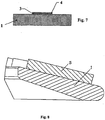
- the ceramic element which is the subject of the present invention, could be in the form of a polygonal frame with a face inclined with respect to the central axis of this element and thus constitute a truncated pyramid.
- the figure 8 illustrates a ceramic ring 1, of frustoconical shape intended to be reported by elastic deformation on a telescope.
- This ring 1 is provided with relief patterns 5, according to the embodiment of the figure 5 .
Landscapes
- Chemical & Material Sciences (AREA)
- Engineering & Computer Science (AREA)
- Ceramic Engineering (AREA)
- Materials Engineering (AREA)
- Structural Engineering (AREA)
- Organic Chemistry (AREA)
- Physical Vapour Deposition (AREA)
- Micromachines (AREA)
- Compositions Of Oxide Ceramics (AREA)
Description
La présente invention se rapporte à un procédé de fabrication d'élément en céramique destiné à être rapporté sur une boîte de montre, dont la surface visible comporte des motifs, ainsi qu'à un élément en céramique obtenu par ce procédé.The present invention relates to a method of manufacturing ceramic element intended to be attached to a watch case, whose visible surface comprises patterns, and to a ceramic element obtained by this method.
Il a déjà été proposé dans le
Etant donné que ces procédés ne permettent pas d'utiliser des matériaux photosensibles, selon des techniques couramment utilisées pour la fabrication de composants électroniques notamment, il ne peuvent donc pas être utilisés pour faire croître sélectivement des motifs tels que des chiffres par électroformage, puisque de tels masques ne résisteraient pas à la température du traitement de fixation des couches au four.Since these methods do not make it possible to use photosensitive materials, according to techniques commonly used for the manufacture of electronic components in particular, they can not therefore be used to selectively grow patterns such as figures by electroforming, since such masks would not withstand the temperature of the process of setting the layers in the oven.
On a également proposé dans le
Le but de la présente invention est de remédier, au moins en partie, aux inconvénients susmentionnés.The object of the present invention is to overcome, at least in part, the aforementioned drawbacks.
A cet effet, cette invention a tout d'abord pour objet un procédé de fabrication d'un élément en céramique destiné à être rapporté sur une boîte de montre et dont la surface visible présente des motifs, selon la revendication 1. Elle a ensuite pour objet un élément en céramique, selon la revendication 4.For this purpose, this invention firstly relates to a method of manufacturing a ceramic element intended to be attached to a watch case and whose visible surface has patterns, according to
L'avantage essentiel de cette invention est de permettre la formation sélective de motifs, sans aucune limitation de forme, donnant naissance à un produit nouveau, offrant des possibilités esthétiques originales, permettant de renouveler et d'améliorer l'aspect des montres, en particulier celui des montres à lunettes fixes et tournantes.The essential advantage of this invention is to allow the selective formation of patterns, without any limitation of shape, giving rise to a new product, offering original aesthetic possibilities, to renew and improve the appearance of watches, in particular fixed and rotating glasses.
Le procédé selon la présente invention permet d'obtenir une excellente adhésion des motifs en relief à la surface de l'élément en céramique, ce qui présente une grande importance, surtout lorsque les motifs sont en relief, puisqu'une boîte de montre-bracelet en particulier est très exposée à toutes sortes d'agressions externes.The method according to the present invention makes it possible to obtain excellent adhesion of the relief patterns to the surface of the ceramic element, which is of great importance, especially when the patterns are in relief, since a wristwatch case in particular is very exposed to all kinds of external aggression.
Avantageusement, la surface visible sur laquelle les motifs sont formés est une surface tronconique ou en forme de tronc de pyramide, qui nécessite de ce fait une technique de masquage particulière.Advantageously, the visible surface on which the patterns are formed is a frustoconical or truncated pyramid surface, which therefore requires a particular masking technique.
D'autres particularités et avantages apparaîtront au cours de la description qui suit et qui sera faite en se référant aux dessins annexés qui illustrent, schématiquement et à titre d'exemple, une forme d'exécution et une variante de la mise en oeuvre du procédé objet de la présente invention, ainsi que les éléments en céramiques obtenus par ce procédé.
- Les
figures 1 à 4 illustrent différentes phases du procédé de préparation d'un élément en céramique vu en coupe, destiné à être rapporté sur une boîte de montre, objet de la présente invention; - les
figures 5 et 6 illustrent une forme d'exécution de formation de motifs en relief; - la
figure 7 illustre une variante pour l'obtention de motifs à la surface de l'élément en céramique; - la
figure 8 est une vue partielle en coupe d'un anneau en céramique pour lunette, selon la présente invention.
- The
Figures 1 to 4 illustrate different phases of the method of preparing a ceramic element seen in section, intended to be attached to a watch case object of the present invention; - the
Figures 5 and 6 illustrate an embodiment of pattern formation in relief; - the
figure 7 illustrates a variant for obtaining patterns on the surface of the ceramic element; - the
figure 8 is a partial sectional view of a ceramic bezel ring, according to the present invention.
La
On applique un masque sur cette couche 2 de polymère photosensible type RISTON® MM150, de manière à insoler sélectivement cette couche 2 sous une lumière UV pour polymériser les parties de la couche 2 de polymère photosensibles qui doivent rester sur le substrat 1. On développe alors cette couche 2 dans un bain de Na2CO3 à 0,85% selon les indications du fournisseur du polymère photosensible, pour dissoudre les parties non insolées de la couche 2 pour mettre à nu des portions de surfaces 1a du substrat 1. Ces portions présentent les formes choisies pour la formation des motifs, comme illustré par la
Il y a lieu de remarquer que dans les exemples illustrés, le substrat 1 représenté en coupe par les
Pour cette raison, le masque utilisé pour la formation des motifs dans la couche de polymère 2 n'est pas un masque classique, mais un masque en polymère, thermoformé pour lui donner une forme complémentaire à celle du substrat en céramique. Ce masque en polymère qui présente une certaine souplesse est appliqué sur la couche 2 avec une pression suffisante pour qu'il épouse cette couche 2 sur toute sa surface.For this reason, the mask used for forming the patterns in the
Une fois cette opération de formation des motifs effectuée, on dispose le substrat 1 ainsi revêtu sélectivement par la couche 2, dans une enceinte de revêtement sous vide, dans laquelle une première couche d'accrochage 3 de Ti, Ta, Cr ou Th d'au moins 100 nm est déposée (
Tout en maintenant le vide dans l'enceinte de dépôt, on forme une seconde couche 4 (
L'équipement utilisé pour effectuer le dépôt sous vide par pulvérisation cathodique au magnétron comprend:
- une enceinte cylindrique en acier inoxydable avec système de pompage turbomoléculaire et pompe rotative à palettes;
- un porte-substrat de type carrousel à axe de rotation vertical et substrats positionnés verticalement. Possibilité de réaliser une pulvérisation cathodique RF polarisée sur le porte-substrat;
- deux cathodes magnétrons rectangulaires verticales montées face au carrousel selon un angle de 120° par rapport à l'axe du carrousel;
- deux cathodes:
- une cible Ti99,99
- une cible Au99,99
- une alimentation des cathodes par un générateur RF 13,56 MHz de 600 W avec une boîte d'accord d'impédance manuel;
- une alimentation en gaz (pureté: 5,7-6,0) par débitmètre de masse;
- un contrôle de pression par jauge Penning pour le contrôle du vide limite et par jauge capacitive (mesure absolue) pour le contrôle de la pression de travail.
- a cylindrical stainless steel enclosure with turbomolecular pumping system and rotary vane pump;
- a carousel-type substrate holder with vertical axis of rotation and substrates positioned vertically. Possibility of polarized RF sputtering on the substrate holder;
- two vertical rectangular magnetron cathodes mounted facing the carousel at an angle of 120 ° to the carousel axis;
- two cathodes:
- a 99.99 Ti target
- a target at 99.99
- a cathode supply by a 13.56 MHz 600 W RF generator with manual impedance tuning box;
- a gas supply (purity: 5.7-6.0) by mass flow meter;
- a pressure control by Penning gauge for the control of the limit vacuum and by capacitive gauge (absolute measurement) for the control of the working pressure.
Les pièces ont été nettoyées dans un bain aux ultrasons dans un mélange de 20% d'alcool isopropylique et de 80% d'eau déionisée, pendant cinq minutes. Séchage au pistolet à azote.The pieces were cleaned in an ultrasonic bath in a mixture of 20% isopropyl alcohol and 80% deionized water for five minutes. Drying with a nitrogen gun.
Les substrats sont décapés par mise sous vide de l'enceinte et pompage jusqu'à une pression inférieure à 5 × 10⁻² Pa. Un nettoyage ionique de la surface des substrats est exécuté par pulvérisation inversée:
- puissance RF sur porte-substrat:> 100 W
- flux d'argon:> 15 cm3/min
- flux d'oxygène:> 5 cm3/min
- pression totale:< 5 Pa
- durée: 20-30 min
- RF power on substrate holder:> 100 W
- argon flow:> 15 cm 3 / min
- oxygen flow:> 5 cm 3 / min
- total pressure: <5 Pa
- duration: 20-30 min
Les conditions de dépôt de la sous-couche de titane sont les suivantes:
- puissance RF sur la cathode:> 150 W
- flux d'argon:> 5 cm3/min
- pression d'argon:< 5 Pa
- l'épaisseur de la couche est >100 nm, de préférence >100 nm et <1500 nm
- RF power on the cathode:> 150 W
- argon flow:> 5 cm 3 / min
- argon pressure: <5 Pa
- the thickness of the layer is> 100 nm, preferably> 100 nm and <1500 nm
Tout en maintenant le vide dans l'enceinte, les substrats sont déplacés par rotation du carrousel vers une petite cathode équipée de la cible Au99,99. Les conditions du dépôt sont les suivantes:
- puissance RF sur la cathode:> 50 W
- flux d'argon:> 10 cm3/min
- pression d'argon:< 5 Pa
- l'épaisseur de la couche est >100 nm, de préférence, >500 nm et <15 µm
- RF power on the cathode:> 50 W
- argon flow:> 10 cm 3 / min
- argon pressure: <5 Pa
- the thickness of the layer is> 100 nm, preferably> 500 nm and <15 μm
Les substrats ainsi obtenus sont entièrement recouverts de la couche d'accrochage en titane recouverte de la couche d'or, comme illustré par la
Suite au dépôt de cette seconde couche 4, on sort le substrat de l'enceinte de dépôt sous vide et on a le choix entre deux solutions.Following the deposition of this
Selon une première forme d'exécution, on soumet le substrat 1 sélectivement revêtu de la couche de polymère 2 et des couches 3 et 4 (
Selon une deuxième forme d'exécution illustrée par la
En variante, au lieu d'être en forme d'anneau tronconique, l'élément en céramique, objet de la présente invention, pourrait être en forme de cadre polygonal à face inclinée par rapport à l'axe central de cet élément et constituer ainsi un tronc de pyramide.As a variant, instead of being in the form of a frustoconical ring, the ceramic element, which is the subject of the present invention, could be in the form of a polygonal frame with a face inclined with respect to the central axis of this element and thus constitute a truncated pyramid.
La
Claims (9)
- A process for manufacturing a ceramic element intended to be fitted onto a watch case and the visible surface of which has features, wherein a soluble layer (2) of a photosensitive polymer is selectively deposited on said visible surface, the thickness of said soluble layer being at least equal to the height of said features, a first tie layer (3) of the Ti, Ta, Cr or Th type is vacuum-deposited by magnetron sputtering with a thickness of at least 100 nm by physical vapor deposition (PVD) on said surface thus selectively coated, followed, without venting atmosphere, by PVD deposition of said second layer (4) made of Au, Pt, Ag, Ni, Pd, TiN, CrN, ZrN or alloys thereof with a thickness of at least 100 nm, and then said soluble layer (2) is dissolved.
- The process as claimed in claim 1, in which, before said soluble layer (2) is dissolved, an additional layer (5) of a noble metal or an alloy of noble metals is deposited by electroforming.
- The process as claimed in claim 2, in which a thermoplastic polymer mask produced by thermoforming is applied to said photosensitive polymer layer (2).
- A ceramic element intended to be fitted onto a watch case and the visible surface of which has features, wherein these features are fixed to this surface via a first Ti, Ta, Cr or Th tie layer (3) at least 100 nm in thickness, covered by at least one second layer (4) of the group comprising Au, Ag, CrN, Ni, Pt, TiN, ZrN, Pd or alloys thereof, with a thickness of at least 100 nm.
- The ceramic element as claimed in claim 4, the shape of which is circular, the face forming said visible surface being of frustoconical shape.
- The ceramic element as claimed in claim 4, the shape of which is that of a polygonal frame, that face forming said visible surface being of frustopyramidal shape.
- The ceramic element as claimed in one of claims 4 to 6, in which said ceramic is ZrO2, Al2O3 or a mixture of the two.
- The ceramic element as claimed in one of claims 4 to 7, in which said features are formed by an additional layer (5) with a thickness of at least 0.10 mm, made of the same metal or alloy as said second layer (4).
- A watch case comprising a ceramic element according to one of claims 4 to 8.
Priority Applications (7)
| Application Number | Priority Date | Filing Date | Title |
|---|---|---|---|
| EP03405924.6A EP1548525B2 (en) | 2003-12-23 | 2003-12-23 | Ceramic element for watch case and method of manufacturing the same |
| CNB2004100819067A CN100507765C (en) | 2003-12-23 | 2004-12-16 | Method for producing a ceramic element for a watch case and element obtained by this method |
| JP2004371658A JP2005181341A (en) | 2003-12-23 | 2004-12-22 | Method for manufacturing ceramic member of timepiece case, and member obtained by the same |
| US11/061,289 US7628894B2 (en) | 2003-12-23 | 2005-02-18 | Process for manufacturing a ceramic element for a watch case and element obtained by this process |
| HK05105899.6A HK1073506B (en) | 2005-07-12 | Ceramic element for watch case and method of manufacturing the same | |
| US12/603,792 US8282270B2 (en) | 2003-12-23 | 2009-10-22 | Process for manufacturing a ceramic element for a watch case and element obtained by this process |
| JP2011138570A JP4921603B2 (en) | 2003-12-23 | 2011-06-22 | Method for manufacturing ceramic member for watch case and member obtained by the method |
Applications Claiming Priority (1)
| Application Number | Priority Date | Filing Date | Title |
|---|---|---|---|
| EP03405924.6A EP1548525B2 (en) | 2003-12-23 | 2003-12-23 | Ceramic element for watch case and method of manufacturing the same |
Publications (3)
| Publication Number | Publication Date |
|---|---|
| EP1548525A1 EP1548525A1 (en) | 2005-06-29 |
| EP1548525B1 EP1548525B1 (en) | 2013-08-14 |
| EP1548525B2 true EP1548525B2 (en) | 2017-08-16 |
Family
ID=34530866
Family Applications (1)
| Application Number | Title | Priority Date | Filing Date |
|---|---|---|---|
| EP03405924.6A Expired - Lifetime EP1548525B2 (en) | 2003-12-23 | 2003-12-23 | Ceramic element for watch case and method of manufacturing the same |
Country Status (4)
| Country | Link |
|---|---|
| US (2) | US7628894B2 (en) |
| EP (1) | EP1548525B2 (en) |
| JP (2) | JP2005181341A (en) |
| CN (1) | CN100507765C (en) |
Families Citing this family (16)
| Publication number | Priority date | Publication date | Assignee | Title |
|---|---|---|---|---|
| US7781679B1 (en) * | 2005-09-09 | 2010-08-24 | Magnecomp Corporation | Disk drive suspension via formation using a tie layer and product |
| US8553364B1 (en) | 2005-09-09 | 2013-10-08 | Magnecomp Corporation | Low impedance, high bandwidth disk drive suspension circuit |
| US7829793B2 (en) * | 2005-09-09 | 2010-11-09 | Magnecomp Corporation | Additive disk drive suspension manufacturing using tie layers for vias and product thereof |
| US8395866B1 (en) | 2005-09-09 | 2013-03-12 | Magnecomp Corporation | Resilient flying lead and terminus for disk drive suspension |
| CH714243B1 (en) * | 2006-10-03 | 2019-04-15 | Swatch Group Res & Dev Ltd | Electroforming process and part or layer obtained by this method. |
| CH710184B1 (en) | 2007-09-21 | 2016-03-31 | Aliprandini Laboratoires G | Process for obtaining a yellow gold alloy deposit by electroplating without the use of toxic metals or metalloids. |
| EP2312021B1 (en) | 2009-10-15 | 2020-03-18 | The Swatch Group Research and Development Ltd. | Method for obtaining a deposit of a yellow gold alloy by galvanoplasty without using toxic metals |
| EP2823080A1 (en) * | 2012-03-07 | 2015-01-14 | Seco Tools AB | A body with a metal based nitride layer and a method for coating the body |
| CN102912292B (en) * | 2012-10-18 | 2014-05-28 | 东南大学 | High temperature resistance bonding coating used for surface of nickel base alloy fastener and preparation method thereof |
| US9284485B2 (en) | 2012-11-07 | 2016-03-15 | Rolex Sa | Persistent phosphorescent composite material |
| CN103572233B (en) * | 2013-10-16 | 2015-09-23 | 中国科学院宁波材料技术与工程研究所 | A kind of Noble metal ceramic film and preparation method thereof |
| US9919971B2 (en) | 2013-12-27 | 2018-03-20 | Tosoh Corporation | Zirconia sintered body and use thereof |
| EP3034461B1 (en) * | 2014-12-19 | 2020-07-01 | Rolex Sa | Production of a multi-level clock component |
| FR3077302B1 (en) * | 2018-01-29 | 2019-12-27 | Avipo | DEPOSIT OF PVD AT THE BOTTOM OF ENGRAVING |
| EP3536826B1 (en) * | 2018-03-09 | 2021-04-28 | The Swatch Group Research and Development Ltd | Method for producing a metal decoration on a dial and dial obtained according to said method |
| EP3575447A1 (en) * | 2018-05-28 | 2019-12-04 | The Swatch Group Research and Development Ltd | Method for producing a metal decoration on a dial and dial obtained according to said method |
Citations (17)
| Publication number | Priority date | Publication date | Assignee | Title |
|---|---|---|---|---|
| DE2533524A1 (en) † | 1975-07-26 | 1977-03-10 | Licentia Gmbh | Forming strongly adhering metal coating on glass or ceramic - by applying intermediate layer contg. copper and its oxides, and heating |
| US4213840A (en) † | 1978-11-13 | 1980-07-22 | Avantek, Inc. | Low-resistance, fine-line semiconductor device and the method for its manufacture |
| US4226082A (en) † | 1976-06-07 | 1980-10-07 | Nobuo Nishida | Ornamental part for watches and method of producing the same |
| JPS60141647A (en) † | 1983-12-27 | 1985-07-26 | Seiko Instr & Electronics Ltd | Decorating method of cover glass |
| EP0221492A2 (en) † | 1985-11-04 | 1987-05-13 | Asulab S.A. | Article coated with a wear-resistant film of a precious metal |
| WO1987004812A1 (en) † | 1986-02-04 | 1987-08-13 | Preci-Coat S.A. | Method for depositing on a substrate a wear-resistant decorative coating layer, and object produced according to this method |
| US4699850A (en) † | 1985-03-19 | 1987-10-13 | Seiko Instruments & Electronics Ltd. | Ornamental part |
| US4943486A (en) † | 1987-04-01 | 1990-07-24 | Seiko Epson Corporation | Coated article and method of production |
| WO1991014017A1 (en) † | 1990-03-09 | 1991-09-19 | Kennametal Inc. | Physical vapor deposition of titanium nitride on a nonconductive substrate |
| JPH046263A (en) † | 1990-04-24 | 1992-01-10 | Namiki Precision Jewel Co Ltd | Method for ornamenting noble metal to sapphire |
| JPH0725199A (en) † | 1993-07-12 | 1995-01-27 | Namiki Precision Jewel Co Ltd | How to decorate sapphire with precious metals |
| EP0686706A1 (en) † | 1993-12-28 | 1995-12-13 | Citizen Watch Co. Ltd. | White decorative part and process for producing the same |
| US5972233A (en) † | 1996-01-31 | 1999-10-26 | Refractal Design, Inc. | Method of manufacturing a decorative article |
| EP1286234A1 (en) † | 2000-04-20 | 2003-02-26 | Trigger Co., Ltd. | Radiowave wristwatch case |
| JP2003253473A (en) † | 2001-12-28 | 2003-09-10 | Citizen Watch Co Ltd | Ornament having white coating film and manufacturing method thereof |
| JP2003268568A (en) † | 2002-01-09 | 2003-09-25 | Citizen Watch Co Ltd | Ornament with white film, and its manufacturing method |
| CH702127B1 (en) † | 2007-05-25 | 2011-05-13 | Paul Hartzband | Timepiece fitted with a round variable hours. |
Family Cites Families (26)
| Publication number | Priority date | Publication date | Assignee | Title |
|---|---|---|---|---|
| CH573139B5 (en) * | 1974-01-18 | 1976-02-27 | Far Fab Assortiments Reunies | |
| JPS55135769A (en) * | 1979-04-11 | 1980-10-22 | Kawaguchiko Seimitsu Kk | Manufacture of dial for watch |
| JPS55141569A (en) * | 1979-04-24 | 1980-11-05 | Kawaguchiko Seimitsu Kk | Manufacture of dial plate of watch |
| CH641313GA3 (en) * | 1980-05-31 | 1984-02-29 | ||
| US4397566A (en) * | 1982-05-04 | 1983-08-09 | Montres Rado S.A. | Wrist-watch casing |
| US4512863A (en) * | 1983-09-09 | 1985-04-23 | Ppg Industries, Inc. | Stainless steel primer for sputtered films |
| US4565616A (en) * | 1984-04-30 | 1986-01-21 | Ppg Industries, Inc. | Method for producing a photoelectroforming mandrel |
| EP0230853A1 (en) * | 1986-01-20 | 1987-08-05 | W. Blösch AG | Process for the realization of a brazeable coating of an alloy on a preferably oxide-ceramic substrate |
| US5100714A (en) * | 1986-07-24 | 1992-03-31 | Ceramic Packaging, Inc. | Metallized ceramic substrate and method therefor |
| US5058799A (en) * | 1986-07-24 | 1991-10-22 | Zsamboky Kalman F | Metallized ceramic substrate and method therefor |
| US4886766A (en) * | 1987-08-10 | 1989-12-12 | Lanxide Technology Company, Lp | Method of making ceramic composite articles and articles made thereby |
| US5082700A (en) * | 1987-08-10 | 1992-01-21 | Lanxide Technology Company, Lp | Method of making ceramic composite articles and articles made thereby |
| JPH0192356A (en) * | 1987-09-30 | 1989-04-11 | Pentel Kk | Ornamental body and its production |
| US5157258A (en) * | 1989-08-21 | 1992-10-20 | Rockwell International Corporation | Multicolor infrared focal plane arrays |
| DE4009151A1 (en) * | 1990-03-22 | 1991-09-26 | Leybold Ag | DEVICE FOR COATING SUBSTRATES BY CATODE SCREENING |
| US5358597A (en) * | 1991-09-04 | 1994-10-25 | Gte Laboratories Incorporated | Method of protecting aluminum nitride circuit substrates during electroless plating using sol-gel oxide films and article made therefrom |
| US5331608A (en) * | 1992-03-31 | 1994-07-19 | Citizen Watch Co., Ltd. | Electronic watch with an antenna for a receiving device |
| DE4213041C1 (en) * | 1992-04-21 | 1993-06-09 | W.C. Heraeus Gmbh, 6450 Hanau, De | |
| US5912064A (en) * | 1995-04-07 | 1999-06-15 | Citizen Watch Co., Ltd. | Dial plate for solar battery powered watch |
| JPH09127261A (en) * | 1995-11-01 | 1997-05-16 | Kawaguchiko Seimitsu Kk | Dial for time piece |
| EP0844539B1 (en) * | 1996-11-22 | 2003-11-19 | Montres Rado S.A. | Decorative element particularly component of a timepiece |
| US6502982B1 (en) * | 1998-06-05 | 2003-01-07 | Montres Rado Sa | Structural component made of hard material for a wristwatch |
| JP3957920B2 (en) * | 1998-06-11 | 2007-08-15 | キヤノン株式会社 | Inkjet head manufacturing method |
| TW517180B (en) * | 2001-02-23 | 2003-01-11 | Swatch Group Man Serv Ag | Timepiece with analogue display of time related information based on a decimal system |
| TW589167B (en) * | 2001-08-29 | 2004-06-01 | Rado Montres Sa | Link for watch bracelet |
| EP1459644B1 (en) * | 2001-12-28 | 2011-03-30 | Citizen Holdings Co., Ltd. | Decorative article having white coating and method for manufacture thereof |
-
2003
- 2003-12-23 EP EP03405924.6A patent/EP1548525B2/en not_active Expired - Lifetime
-
2004
- 2004-12-16 CN CNB2004100819067A patent/CN100507765C/en not_active Expired - Lifetime
- 2004-12-22 JP JP2004371658A patent/JP2005181341A/en not_active Withdrawn
-
2005
- 2005-02-18 US US11/061,289 patent/US7628894B2/en not_active Expired - Lifetime
-
2009
- 2009-10-22 US US12/603,792 patent/US8282270B2/en not_active Expired - Lifetime
-
2011
- 2011-06-22 JP JP2011138570A patent/JP4921603B2/en not_active Expired - Lifetime
Patent Citations (17)
| Publication number | Priority date | Publication date | Assignee | Title |
|---|---|---|---|---|
| DE2533524A1 (en) † | 1975-07-26 | 1977-03-10 | Licentia Gmbh | Forming strongly adhering metal coating on glass or ceramic - by applying intermediate layer contg. copper and its oxides, and heating |
| US4226082A (en) † | 1976-06-07 | 1980-10-07 | Nobuo Nishida | Ornamental part for watches and method of producing the same |
| US4213840A (en) † | 1978-11-13 | 1980-07-22 | Avantek, Inc. | Low-resistance, fine-line semiconductor device and the method for its manufacture |
| JPS60141647A (en) † | 1983-12-27 | 1985-07-26 | Seiko Instr & Electronics Ltd | Decorating method of cover glass |
| US4699850A (en) † | 1985-03-19 | 1987-10-13 | Seiko Instruments & Electronics Ltd. | Ornamental part |
| EP0221492A2 (en) † | 1985-11-04 | 1987-05-13 | Asulab S.A. | Article coated with a wear-resistant film of a precious metal |
| WO1987004812A1 (en) † | 1986-02-04 | 1987-08-13 | Preci-Coat S.A. | Method for depositing on a substrate a wear-resistant decorative coating layer, and object produced according to this method |
| US4943486A (en) † | 1987-04-01 | 1990-07-24 | Seiko Epson Corporation | Coated article and method of production |
| WO1991014017A1 (en) † | 1990-03-09 | 1991-09-19 | Kennametal Inc. | Physical vapor deposition of titanium nitride on a nonconductive substrate |
| JPH046263A (en) † | 1990-04-24 | 1992-01-10 | Namiki Precision Jewel Co Ltd | Method for ornamenting noble metal to sapphire |
| JPH0725199A (en) † | 1993-07-12 | 1995-01-27 | Namiki Precision Jewel Co Ltd | How to decorate sapphire with precious metals |
| EP0686706A1 (en) † | 1993-12-28 | 1995-12-13 | Citizen Watch Co. Ltd. | White decorative part and process for producing the same |
| US5972233A (en) † | 1996-01-31 | 1999-10-26 | Refractal Design, Inc. | Method of manufacturing a decorative article |
| EP1286234A1 (en) † | 2000-04-20 | 2003-02-26 | Trigger Co., Ltd. | Radiowave wristwatch case |
| JP2003253473A (en) † | 2001-12-28 | 2003-09-10 | Citizen Watch Co Ltd | Ornament having white coating film and manufacturing method thereof |
| JP2003268568A (en) † | 2002-01-09 | 2003-09-25 | Citizen Watch Co Ltd | Ornament with white film, and its manufacturing method |
| CH702127B1 (en) † | 2007-05-25 | 2011-05-13 | Paul Hartzband | Timepiece fitted with a round variable hours. |
Also Published As
| Publication number | Publication date |
|---|---|
| CN100507765C (en) | 2009-07-01 |
| US20100110841A1 (en) | 2010-05-06 |
| US20060011471A1 (en) | 2006-01-19 |
| CN1637662A (en) | 2005-07-13 |
| US7628894B2 (en) | 2009-12-08 |
| JP2011191321A (en) | 2011-09-29 |
| US8282270B2 (en) | 2012-10-09 |
| EP1548525A1 (en) | 2005-06-29 |
| JP2005181341A (en) | 2005-07-07 |
| EP1548525B1 (en) | 2013-08-14 |
| JP4921603B2 (en) | 2012-04-25 |
| HK1073506A1 (en) | 2005-10-07 |
Similar Documents
| Publication | Publication Date | Title |
|---|---|---|
| EP1548524B1 (en) | Ceramic element for watch case and method of manufacturing the same | |
| EP1548525B2 (en) | Ceramic element for watch case and method of manufacturing the same | |
| EP0038294B1 (en) | Method of depositing a hard coating of a metal, deposition target for such a method and piece of jewellery comprising such a coating | |
| EP3078436B1 (en) | Method for manufacturing a clock component | |
| EP3339980A1 (en) | Method for producing a pattern on a timepiece and timepiece | |
| EP2354083B1 (en) | Micromechanical device encapsulation process with a mechanically reinforced package cap | |
| EP2659307B1 (en) | Process for fabricating high-precision objects by high-resolution lithography and dry deposition and objects thus obtained | |
| EP1672436B1 (en) | Watch dial and manufacturing methods for such a dial | |
| CH710716A2 (en) | Method of manufacturing a part with at least one decoration | |
| EP3764169B1 (en) | Method for frosting some parts of a silicon timepiece component | |
| EP0627330B1 (en) | Process for making engraved markings covered with contrasting material | |
| EP0411079B1 (en) | Method for the deposition of at least one thickness of at least one decorative material to an object, and decorative object obtained by such method | |
| JP4909477B2 (en) | Decorative member and method of manufacturing decorative member | |
| CH715191B1 (en) | Process for decorating a watch exterior component. | |
| HK1073506B (en) | Ceramic element for watch case and method of manufacturing the same | |
| EP4524288A1 (en) | Method for decorating a substrate by depositing a masking layer by sol-gel method in order to produce a trim part | |
| CH721122A2 (en) | METHOD FOR DECORATING A SUBSTRATE BY DEPOSITING A MASKING LAYER BY SOL-GEL METHOD IN ORDER TO PRODUCE A COVERING PART | |
| HK1073507B (en) | Ceramic element for watch case and method of manufacturing the same | |
| CH720105A2 (en) | METHOD FOR MANUFACTURING A WATCH COMPONENT | |
| EP2833204A1 (en) | Method for treating a layer of photosensitive resin and method for manufacturing a metal component |
Legal Events
| Date | Code | Title | Description |
|---|---|---|---|
| PUAI | Public reference made under article 153(3) epc to a published international application that has entered the european phase |
Free format text: ORIGINAL CODE: 0009012 |
|
| AK | Designated contracting states |
Kind code of ref document: A1 Designated state(s): AT BE BG CH CY CZ DE DK EE ES FI FR GB GR HU IE IT LI LU MC NL PT RO SE SI SK TR |
|
| AX | Request for extension of the european patent |
Extension state: AL LT LV MK |
|
| REG | Reference to a national code |
Ref country code: HK Ref legal event code: DE Ref document number: 1073506 Country of ref document: HK |
|
| 17P | Request for examination filed |
Effective date: 20050922 |
|
| AKX | Designation fees paid |
Designated state(s): CH DE FR GB LI |
|
| 17Q | First examination report despatched |
Effective date: 20070720 |
|
| GRAP | Despatch of communication of intention to grant a patent |
Free format text: ORIGINAL CODE: EPIDOSNIGR1 |
|
| GRAP | Despatch of communication of intention to grant a patent |
Free format text: ORIGINAL CODE: EPIDOSNIGR1 |
|
| GRAS | Grant fee paid |
Free format text: ORIGINAL CODE: EPIDOSNIGR3 |
|
| GRAA | (expected) grant |
Free format text: ORIGINAL CODE: 0009210 |
|
| AK | Designated contracting states |
Kind code of ref document: B1 Designated state(s): CH DE FR GB LI |
|
| REG | Reference to a national code |
Ref country code: GB Ref legal event code: FG4D Free format text: NOT ENGLISH |
|
| REG | Reference to a national code |
Ref country code: CH Ref legal event code: EP |
|
| REG | Reference to a national code |
Ref country code: CH Ref legal event code: NV Representative=s name: MOINAS AND SAVOYE SA, CH |
|
| REG | Reference to a national code |
Ref country code: DE Ref legal event code: R096 Ref document number: 60344711 Country of ref document: DE Effective date: 20131010 |
|
| REG | Reference to a national code |
Ref country code: HK Ref legal event code: GR Ref document number: 1073506 Country of ref document: HK |
|
| PLBI | Opposition filed |
Free format text: ORIGINAL CODE: 0009260 |
|
| 26 | Opposition filed |
Opponent name: G. ET F. CHATELAIN SA Effective date: 20140514 |
|
| PLAX | Notice of opposition and request to file observation + time limit sent |
Free format text: ORIGINAL CODE: EPIDOSNOBS2 |
|
| REG | Reference to a national code |
Ref country code: DE Ref legal event code: R026 Ref document number: 60344711 Country of ref document: DE Effective date: 20140514 |
|
| PLBB | Reply of patent proprietor to notice(s) of opposition received |
Free format text: ORIGINAL CODE: EPIDOSNOBS3 |
|
| REG | Reference to a national code |
Ref country code: FR Ref legal event code: PLFP Year of fee payment: 13 |
|
| REG | Reference to a national code |
Ref country code: CH Ref legal event code: PFA Owner name: ROLEX SA, CH Free format text: FORMER OWNER: ROLEX SA, CH |
|
| REG | Reference to a national code |
Ref country code: FR Ref legal event code: PLFP Year of fee payment: 14 |
|
| PUAH | Patent maintained in amended form |
Free format text: ORIGINAL CODE: 0009272 |
|
| STAA | Information on the status of an ep patent application or granted ep patent |
Free format text: STATUS: PATENT MAINTAINED AS AMENDED |
|
| 27A | Patent maintained in amended form |
Effective date: 20170816 |
|
| AK | Designated contracting states |
Kind code of ref document: B2 Designated state(s): CH DE FR GB LI |
|
| REG | Reference to a national code |
Ref country code: DE Ref legal event code: R102 Ref document number: 60344711 Country of ref document: DE |
|
| REG | Reference to a national code |
Ref country code: CH Ref legal event code: AELC |
|
| REG | Reference to a national code |
Ref country code: FR Ref legal event code: PLFP Year of fee payment: 15 |
|
| PGFP | Annual fee paid to national office [announced via postgrant information from national office to epo] |
Ref country code: GB Payment date: 20221219 Year of fee payment: 20 Ref country code: FR Payment date: 20221220 Year of fee payment: 20 Ref country code: DE Payment date: 20220624 Year of fee payment: 20 |
|
| PGFP | Annual fee paid to national office [announced via postgrant information from national office to epo] |
Ref country code: CH Payment date: 20221229 Year of fee payment: 20 |
|
| P01 | Opt-out of the competence of the unified patent court (upc) registered |
Effective date: 20230528 |
|
| REG | Reference to a national code |
Ref country code: DE Ref legal event code: R071 Ref document number: 60344711 Country of ref document: DE |
|
| REG | Reference to a national code |
Ref country code: CH Ref legal event code: PL |
|
| REG | Reference to a national code |
Ref country code: GB Ref legal event code: PE20 Expiry date: 20231222 |
|
| PG25 | Lapsed in a contracting state [announced via postgrant information from national office to epo] |
Ref country code: GB Free format text: LAPSE BECAUSE OF EXPIRATION OF PROTECTION Effective date: 20231222 |
|
| PG25 | Lapsed in a contracting state [announced via postgrant information from national office to epo] |
Ref country code: GB Free format text: LAPSE BECAUSE OF EXPIRATION OF PROTECTION Effective date: 20231222 |