EP1548470B1 - Organic electroluminescence element comprising a lens array sheet - Google Patents
Organic electroluminescence element comprising a lens array sheet Download PDFInfo
- Publication number
- EP1548470B1 EP1548470B1 EP03788087.9A EP03788087A EP1548470B1 EP 1548470 B1 EP1548470 B1 EP 1548470B1 EP 03788087 A EP03788087 A EP 03788087A EP 1548470 B1 EP1548470 B1 EP 1548470B1
- Authority
- EP
- European Patent Office
- Prior art keywords
- pyramid
- organic electroluminescence
- electroluminescence element
- recesses
- set forth
- Prior art date
- Legal status (The legal status is an assumption and is not a legal conclusion. Google has not performed a legal analysis and makes no representation as to the accuracy of the status listed.)
- Expired - Lifetime
Links
Images


Classifications
-
- G—PHYSICS
- G02—OPTICS
- G02B—OPTICAL ELEMENTS, SYSTEMS OR APPARATUS
- G02B1/00—Optical elements characterised by the material of which they are made; Optical coatings for optical elements
- G02B1/04—Optical elements characterised by the material of which they are made; Optical coatings for optical elements made of organic materials, e.g. plastics
- G02B1/041—Lenses
-
- G—PHYSICS
- G02—OPTICS
- G02B—OPTICAL ELEMENTS, SYSTEMS OR APPARATUS
- G02B3/00—Simple or compound lenses
- G02B3/0006—Arrays
- G02B3/0012—Arrays characterised by the manufacturing method
- G02B3/0031—Replication or moulding, e.g. hot embossing, UV-casting, injection moulding
-
- G—PHYSICS
- G02—OPTICS
- G02B—OPTICAL ELEMENTS, SYSTEMS OR APPARATUS
- G02B3/00—Simple or compound lenses
- G02B3/0006—Arrays
- G02B3/0037—Arrays characterized by the distribution or form of lenses
- G02B3/0043—Inhomogeneous or irregular arrays, e.g. varying shape, size, height
-
- G—PHYSICS
- G02—OPTICS
- G02B—OPTICAL ELEMENTS, SYSTEMS OR APPARATUS
- G02B3/00—Simple or compound lenses
- G02B3/0006—Arrays
- G02B3/0037—Arrays characterized by the distribution or form of lenses
- G02B3/0056—Arrays characterized by the distribution or form of lenses arranged along two different directions in a plane, e.g. honeycomb arrangement of lenses
-
- G—PHYSICS
- G02—OPTICS
- G02B—OPTICAL ELEMENTS, SYSTEMS OR APPARATUS
- G02B5/00—Optical elements other than lenses
- G02B5/02—Diffusing elements; Afocal elements
- G02B5/0205—Diffusing elements; Afocal elements characterised by the diffusing properties
- G02B5/021—Diffusing elements; Afocal elements characterised by the diffusing properties the diffusion taking place at the element's surface, e.g. by means of surface roughening or microprismatic structures
-
- G—PHYSICS
- G02—OPTICS
- G02B—OPTICAL ELEMENTS, SYSTEMS OR APPARATUS
- G02B5/00—Optical elements other than lenses
- G02B5/02—Diffusing elements; Afocal elements
- G02B5/0205—Diffusing elements; Afocal elements characterised by the diffusing properties
- G02B5/021—Diffusing elements; Afocal elements characterised by the diffusing properties the diffusion taking place at the element's surface, e.g. by means of surface roughening or microprismatic structures
- G02B5/0231—Diffusing elements; Afocal elements characterised by the diffusing properties the diffusion taking place at the element's surface, e.g. by means of surface roughening or microprismatic structures the surface having microprismatic or micropyramidal shape
-
- G—PHYSICS
- G02—OPTICS
- G02B—OPTICAL ELEMENTS, SYSTEMS OR APPARATUS
- G02B5/00—Optical elements other than lenses
- G02B5/02—Diffusing elements; Afocal elements
- G02B5/0268—Diffusing elements; Afocal elements characterized by the fabrication or manufacturing method
-
- H—ELECTRICITY
- H05—ELECTRIC TECHNIQUES NOT OTHERWISE PROVIDED FOR
- H05B—ELECTRIC HEATING; ELECTRIC LIGHT SOURCES NOT OTHERWISE PROVIDED FOR; CIRCUIT ARRANGEMENTS FOR ELECTRIC LIGHT SOURCES, IN GENERAL
- H05B33/00—Electroluminescent light sources
- H05B33/12—Light sources with substantially two-dimensional [2D] radiating surfaces
- H05B33/22—Light sources with substantially two-dimensional [2D] radiating surfaces characterised by the chemical or physical composition or the arrangement of auxiliary dielectric or reflective layers
-
- H—ELECTRICITY
- H10—SEMICONDUCTOR DEVICES; ELECTRIC SOLID-STATE DEVICES NOT OTHERWISE PROVIDED FOR
- H10K—ORGANIC ELECTRIC SOLID-STATE DEVICES
- H10K59/00—Integrated devices, or assemblies of multiple devices, comprising at least one organic light-emitting element covered by group H10K50/00
- H10K59/80—Constructional details
- H10K59/875—Arrangements for extracting light from the devices
- H10K59/879—Arrangements for extracting light from the devices comprising refractive means, e.g. lenses
-
- G—PHYSICS
- G02—OPTICS
- G02B—OPTICAL ELEMENTS, SYSTEMS OR APPARATUS
- G02B5/00—Optical elements other than lenses
- G02B5/04—Prisms
- G02B5/045—Prism arrays
-
- H—ELECTRICITY
- H10—SEMICONDUCTOR DEVICES; ELECTRIC SOLID-STATE DEVICES NOT OTHERWISE PROVIDED FOR
- H10K—ORGANIC ELECTRIC SOLID-STATE DEVICES
- H10K50/00—Organic light-emitting devices
- H10K50/80—Constructional details
- H10K50/85—Arrangements for extracting light from the devices
- H10K50/858—Arrangements for extracting light from the devices comprising refractive means, e.g. lenses
Definitions
- the present invention relates to an organic electroluminescence element comprising a lens array sheet, a process for its production and a display device comprising the element.
- a sheet (lens array sheet) having a lens array formed with a fine concave and convex pattern, such as a prism shape and a Fresnel lens shape, on a surface of a thermoplastic resin mold, such as a transparent plastic, has been increasingly used as an optical part in recent years.
- a method of easily attaining high luminance by using a lens array sheet as a light condensing plate for a liquid crystal display device and condensing a display light in an approximately normal direction has become widely used.
- This method uses a light condensing effect of a prism and is capable of attaining high luminance without increasing an electric power and a thickness of the device, while it has a disadvantage that the luminance drastically declines when being out of the light condensing range.
- the Japanese Unexamined Patent Publication No. 7-261006 proposes to change a refraction index between one surface and the other surface of the prism. Also, the Japanese Unexamined Patent Publication No. 2000-75102 proposes to use as a material of the light condensing plate an alicyclic structure containing thermoplastic resin having a norbornene structure.
- an organic electroluminescence material can be used as a thin film, it is an effective material for making a surface lighting device and a display device thinner and lighter.
- light transmittance of a liquid crystal panel is too low to use it as a backlight of a liquid crystal display device, therefore, the light condensing efficiency has to be furthermore improved comparing with that in a conventional backlight using a cold-cathode tube, etc.
- US2002/0094422 A1 discloses an organic electroluminescent element according to the preamble of claim 1.
- JP 08 8271888 discloses a light control sheet with pyramid shaped recesses.
- An object of the present invention is to provide an organic electroluminescence element comprising a lens array sheet having a wide viewing angle and an improved light condensing efficiency.
- the present inventors confirmed that a line shaped prism lens converges a light only in one direction and that the disadvantages explained above arise.
- a lens array sheet having pyramid-shaped projections and recesses is capable of most effectively condensing even a light from an organic electroluminescence element comparing with ones having projections and recesses in a three-sided pyramid, six-sided pyramid, eight-sided pyramid or conical shape, so that the present invention has completed.
- an organic electroluminescent element according to claim 1.
- a indicates a length of a side forming a bottom surface of a pyramid shape
- b indicates a length of other one side forming the bottom surface of the pyramid shape
- c indicates a height of pyramid-shaped projections or recesses
- ⁇ indicates a base angle of side surfaces of the pyramid shape
- 1 indicates pyramid-shaped projection or recess
- 2 indicates a lens array sheet
- s indicates a width between pyramid shaped projections or recesses.
- a lens array sheet has pyramid-shaped projections or recesses on a surface (preferably, on one surface) of a transparent base material film.
- a transparent base material film to be used in the present invention is a film shaped mold composed substantially of a transparent resin material.
- the expression "composed substantially of a transparent resin material” means the case of composing all by a transparent resin material and the case of including various additives in accordance with need as far as it is not more than 50 wt% or so with respect to the total amount.
- the transparent resin material polyethylene, polypropylene, polymethylpentene and other linear polyolefin resins; polystyrene and other aromatic vinyl based resins; a norbornene based polymer, a vinyl alicyclic hydrocarbon polymer, a monocyclic olefin based polymer, a cyclic diolefin based polymer and other alicyclic olefin resins; polycarbonate, polyethylene phthalate, polybutylene phthalate, liquid crystal polyester and other polyester based resins; polymethyl methacrylate and other acrylic resins; an acrylonitrile styrene resin, an acrylonitrile styrene butadiene resin and other acrylonitrile based resins; polysulfone, polyether sulfone, polyphenylene sulfide, polyphenylene ether and other polyether based resins; and polyether ether ketone and other ketone based resins;
- a linear polyolefin resin, an alicyclic olefin resin and polyether based resin, etc. are preferable because they easily bring cross-linking reaction by irradiation of an active energy beam and solubility in specific solvents easily changes. Furthermore, an alicyclic olefin resin is the most preferable because of less absorption of visible light and a low water-absorbing property.
- an alicyclic olefin resin a ring-opened polymer of a norbornene based monomer and the hydrogenated product, a ring-opened polymer of other monomer capable of copolymerizing with a norbornene based monomer and the hydrogenated product, an addition polymer of a norbornene based monomer and the hydrogenated product, an additional copolymer with other monomer capable of copolymerizing with a norbornene based monomer and the hydrogenated product and other norbornene based polymers; polyvinylcycloalkane, polyvinylcycloalkene, hydrogenated product of an aromatic vinyl polymer and other vinyl alicyclic hydrocarbon polymer; polycyclopentene, polycyclohexene and other monocyclic olefin based polymers; polycyclohexadiene and other cyclic diolefin based polymers; etc.
- a norbornene based polymer and a vinyl alicyclic hydrocarbon polymer are the most preferable.
- a vinyl alicyclic hydrocarbon polymer may be a copolymer with other monomer (for example, butadiene, isoprene and other vinyl based monomers, etc.) capable of copolymerizing with vinylcycloalkane, vinylcycloalkene and an aromatic vinyl based monomer, etc., and the polymer form may be either of a block polymer and a random polymer.
- a thickness of the transparent base material film is normally 0.05 to 3 mm or so.
- Projections or recesses on a surface of the transparent base material are pyramid shaped.
- the projections or recesses may have a pyramid shape having different base angles of side surfaces or a right pyramid shape wherein all of the bottom angles are the same. Alternately, it may be a pyramid shape wherein an apex angle is cut off.
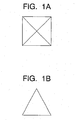
- shapes shown in FIG. 1A, FIG. 1B , FIG. 2A, FIG. 2B , FIG. 3A, FIG. 3B , FIG. 4A and FIG. 4B are the examples but it is not limited to these.
- the bottom surface of the pyramid shape is a rectangular or square shape satisfying the relationship below.
- the relationship is preferably (length “a” of one side) ⁇ (length “b” of other side) ⁇ 10a, more preferably (length “a” of one side) ⁇ (length “b” of other side) ⁇ 5a, further preferably (length “a” of one side) ⁇ (length “b” of other side) ⁇ 2a, particularly preferably (length “a” of one side) ⁇ (length "b” of other side) ⁇ 1.5a.
- the length "a" of one side of the bottom surface of the pyramid shape is not particularly limited but is normally 0.1 ⁇ m to 500 ⁇ m, preferably 0.1 ⁇ m to 100 ⁇ m.
- the length "a” is preferably 0.1 ⁇ m to 20 ⁇ m, so that the liquid crystal is capable of preventing interference by an outside light (so-called moiré).
- the base angle ⁇ of side surfaces of the pyramid shape is preferably 20° to 80°, particularly preferably 30° to 75°.
- a height "c" of the pyramid shape (a length from the bottom surface to the apex angle) is not particularly limited and is preferably 0.2a ⁇ c ⁇ 2a, more preferably 0.5a ⁇ c ⁇ 1.5a with respect to the length "a" of one side of the bottom surface of the pyramid shape.
- directions of the respective projections and recesses may be a regular lattice shape as shown in FIG. 5A , a hound's-tooth check shape as shown in FIG. 5B , or a random shape as shown in FIG. 5C .
- a regular lattice shape or hound's-tooth check shape is preferable for obtaining higher luminance.
- a shape of the respective projections or recesses arranged on the surface of the transparent base material film may be all same or independent shapes from one another.
- a method of forming pyramid-shaped projections or recesses on a surface of the transparent base material film is not particularly limited.
- a method of setting a mold formed with pyramid-shaped projections or recesses to perform injection molding, compression molding or heat-melt molding, such as blow molding (2) a method of using a die formed with pyramid-shaped projections or recesses to perform melt extrusion molding, (3) a so-called 2P method for applying an ultraviolet ray curing resin on a molding surface formed with pyramid-shaped projections or recesses, then, curing the resin by irradiating an ultraviolet ray to transfer a pattern, may be mentioned.
- a method of transferring a pattern by using the above method (1) is preferable.
- a method of producing a mold is not particularly limited. For example, to produce a mold having pyramid-shaped "projections" on its surface, a method of forming a metal layer by stacking a metal by a soldering method or a sputtering method, etc. on a substrate formed with a pyramid-shaped concave pattern, then, peeling the metal layer from the substrate may be mentioned.
- a method of using a mold having pyramid-shaped projections obtained as above and performing mold release processing for bringing the mold surface into contact with potassium bichromate or other oxidizing agent, etc. in accordance with need, then, forming a metal layer by the same method as above by stacking metal, and peeling the metal layer from the mold may be mentioned.
- a method of obtaining a substrate formed with a pyramid-shaped concave pattern is not particularly limited, and a method of using a property that a silicon single crystal substrate is anisotropically etched by an alkaline solution (etching solution) may be mentioned as a preferable example because a fine pattern is easily obtained.
- etching solution alkaline solution
- this method is by (1) stacking an oxidized silicon film and a photo resist film on a silicon substrate in this order, then, forming a pattern on the photoresist film, (2) performing etching on the oxidized silicon layer by an etching solution containing hydrofluoric acid by using the resist pattern as a mask to form a silicon oxide pattern, (3) furthermore, performing anisotropic etching on the silicon substrate by a sodium hydroxide solution or other alkaline etching solution to form pyramid-shaped recesses on the silicon substrate (at this time, the resist pattern can be also removed at a time for it is soluble in the alkaline etching solution), and (4) bringing the finally left silicon oxide pattern into contact with an etching solution containing hydrofluoric acid to remove the silicon oxide pattern, projection or recesses (pattern) is formed on the surface of the silicon substrate.
- a width of a resist pattern to be a mask becomes a width "s" between adjacent projections or recesses on a lens array sheet of the present invention.
- the narrower the width "s" is, the more preferable. It is preferably 50% or less, more preferably 20% or less, further preferably 10% or less and particularly preferably 5% or less with respect to a length "a" of one side of the bottom surface of the pyramid shape.
- a light condensing plate is made by the above lens array sheet.
- An organic electroluminescence element of the present invention is obtained by stacking a transparent electrode layer, such as indium tin oxide (ITO), an organic electroluminescence material layer including an organic element, and a metal electrode layer in this order on the lens array sheet as a transparent substrate.
- a transparent electrode layer such as indium tin oxide (ITO)
- an organic electroluminescence material layer including an organic element and a metal electrode layer in this order
- the lens array sheet functions as a light condensing plate.
- the organic electroluminescence element can be used as a backlight of a liquid crystal display device, etc.
- a positive type photoresist composition (product name: ZPP1700PG) made by ZEON Corporation by spin-coating on a substrate obtained by forming a film of SiO 2 to 300 ⁇ on a silicon, the result was prebaked at 100°C to obtain a resist film of 1.5 ⁇ m on the substrate.
- the obtained resist film was subjected to exposure of 50 mJ/cm 2 by an exposure apparatus "PLA501F” made by Canon Inc. via a mask, development processing was performed by a 2.38% tetramethyl ammonium hydroxide solution for 60 seconds, and then, rinse processing by ultrapure water was performed for 30 seconds.
- the substrate was dried by spin processing and prebaking processing at 120°C was finally performed to obtain a resist pattern on the substrate.
- the thus obtained substrate was dipped in a hydrofluoric acid buffer solution (mixture of 3.6% hydrofluoric hydrofluoric water and 18% hydrofluoric ammonium water by 1:1 (in volume) at 20°C. It will be the same below.) for five minutes to etch SiO 2 , rinsing processing for immersing the etched substrate in pure water for 60 seconds was performed, then, the substrate was dried by spin processing.
- a hydrofluoric acid buffer solution mixture of 3.6% hydrofluoric hydrofluoric water and 18% hydrofluoric ammonium water by 1:1 (in volume) at 20°C. It will be the same below.
- the substrate wherein the oxide silicon film was etched, was immersed in a 30% sodium hydroxide solution for 30 minutes at 80°, immersed in pure water for 60 seconds, then, dried by blowing a dry air, so that pyramid-shaped concave recesses were formed on the silicon substrate.
- the substrate was dipped in a hydrofluoric acid buffer solution for 5 minutes, then, immersed in pure water for 60 seconds, and dried by blowing a dry air, so that a silicon substrate having pyramid-shaped recesses was produced.
- nickel metal was grown by performing electrolytic soldering in an electrolytic solution containing nickel sulfamate as its main component.
- the obtained nickel block (metal layer) was peeled from the silicon substrate, so that a mold (convex mold) formed with pyramid-shaped "'projections" in a hound's-tooth check shape was produced.
- This mold was set in an injection molding apparatus to obtain a lens array sheet (the outside dimension is 40 mm ⁇ 40 mm) having a thickness of about 1 mm by injection molding (resin melt temperature of 285°C, mold temperature of 130°C, and resin filling time of about 0.2 second) using a cycloolefin polymer (ZNR1430R made by ZEON Corporation).
- the obtained lens array sheet was formed on its surface with pyramid-shaped "recesses" having a bottom surface of 20 ⁇ m ⁇ 20 ⁇ m, a base angle of side surfaces of approximately 55° and a height of 14 ⁇ m in a hound's-tooth check shape.
- NPD N,N-di(1-naphthyl)-N,N'-diphenyl-1,1'-diphenyl-1,4-imine
- Alq3 8-hydroxy quinoline aluminum
- the substrate was moved to a metal evaporation chamber while keeping in the system in a vacuum state, and lithium fluoride loaded on a metal board was heated, so that the lithium fluoride was evaporated to be 5 ⁇ on the organic layer.
- aluminum was loaded on another metal board to evaporate it to be a thickness of 1000 ⁇ by the same operation, so that a stacked body, wherein an ITO layer, an organic electroluminescence material layer and a metal electrode layer were stacked, was obtained on the lens array sheet.
- the thus obtained stacked body was attached with a stainless sealing tube applied with an ultraviolet ray curing adhesion in a globe box in a dry nitrogen, and an ultraviolet ray was irradiated to adhere the sealing tube, consequently, an organic electroluminescence element was obtained.
- the mold in the example 1 was used.
- the mold was immersed in a potassium bichromate solution (0.1 wt%) for 30 seconds and mold releasing processing was performed by oxidizing the mold surface, then, a nickel layer (metal layer) was stacked under the same condition as that in the example 1 and the stacked nickel layer was peeled from the mold, so that a mold (concave mold) formed with pyramid-shaped "recesses" having a base angle of side surfaces of approximately 55° and a height of 14 ⁇ m in a hound's-tooth check shape was obtained.
- a lens array sheet was produced in the same way as in the example 1.
- the obtained lens array sheet was formed on its surface with pyramid-shaped "projections" having a bottom surface of 20 ⁇ m ⁇ 20 ⁇ m, a base angle of side surfaces of approximately 55° and a height of 14 ⁇ m in a hound's-tooth check shape.
- an organic electroluminescence element was produced, and the luminance was measured under the same condition.
- the result was 1420 cd/cm 2 . From the result, it was confirmed that luminance of the organic electroluminescence element was improved to about 1.7 times comparing with that in the comparative example 1 by using the lens array sheet of the example 2 as a light condensing plate.
- a viewing angle was confirmed to have a tendency of becoming wider as the luminance improves.
- a lens array sheet exhibits remarkable efficiency in improving luminance as a light condensing plate of an organic electroluminescence element.
- the lens array sheet can be used as an optical part, such as an information recording medium, optical lens, optical filter, light guide plate for a liquid crystal display device and optical sheet, in addition to being used as a light condensing plate of an organic electroluminescence element.
Landscapes
- Physics & Mathematics (AREA)
- General Physics & Mathematics (AREA)
- Optics & Photonics (AREA)
- Engineering & Computer Science (AREA)
- Manufacturing & Machinery (AREA)
- Electroluminescent Light Sources (AREA)
- Moulds For Moulding Plastics Or The Like (AREA)
- Liquid Crystal (AREA)
Description
- The present invention relates to an organic electroluminescence element comprising a lens array sheet, a process for its production and a display device comprising the element.
- There are demands for a surface lighting device used for a display device to have many characteristics, such as high luminance, low power consumption and thin shape. When improving one of these characteristics, it is liable that other performance has to be more or less sacrificed and it has been very difficult to improve all performances at a time.
- To overcome the plurality of challenges, a sheet (lens array sheet) having a lens array formed with a fine concave and convex pattern, such as a prism shape and a Fresnel lens shape, on a surface of a thermoplastic resin mold, such as a transparent plastic, has been increasingly used as an optical part in recent years.
- For example, a method of easily attaining high luminance by using a lens array sheet as a light condensing plate for a liquid crystal display device and condensing a display light in an approximately normal direction has become widely used. This method uses a light condensing effect of a prism and is capable of attaining high luminance without increasing an electric power and a thickness of the device, while it has a disadvantage that the luminance drastically declines when being out of the light condensing range.
- To solve such a disadvantage, the Japanese Unexamined Patent Publication No.
7-261006 2000-75102 - Since an organic electroluminescence material can be used as a thin film, it is an effective material for making a surface lighting device and a display device thinner and lighter. However, light transmittance of a liquid crystal panel is too low to use it as a backlight of a liquid crystal display device, therefore, the light condensing efficiency has to be furthermore improved comparing with that in a conventional backlight using a cold-cathode tube, etc.
- However, when using a prism lens having a line shaped surface, which has been conventionally used as a light condensing plate of a liquid crystal substrate, as a light condensing plate of an organic electroluminescence element, there is a disadvantage that the viewing angle becomes narrow.
-
US2002/0094422 A1 discloses an organic electroluminescent element according to the preamble ofclaim 1.JP 08 8271888 - An object of the present invention is to provide an organic electroluminescence element comprising a lens array sheet having a wide viewing angle and an improved light condensing efficiency.
- The present inventors confirmed that a line shaped prism lens converges a light only in one direction and that the disadvantages explained above arise. As a result that they have been committed themselves to study for attaining an improvement in light convergence, they found that a lens array sheet having pyramid-shaped projections and recesses is capable of most effectively condensing even a light from an organic electroluminescence element comparing with ones having projections and recesses in a three-sided pyramid, six-sided pyramid, eight-sided pyramid or conical shape, so that the present invention has completed.
- According to the present invention, there is provided an organic electroluminescent element according to
claim 1. -
-
FIG. 1A ,FIG. 2A ,FIG. 3A andFIG. 4A are plan views of examples of a pyramid shape; -
FIG. 1B ,FIG. 2B ,FIG. 3B andFIG. 4B are views from the front of the respective examples inFIG. 1A ,FIG. 2A ,FIG. 3A andFIG. 4A ; -
FIG. 5A, FIG. 5B and FIG. 5C are plan views showing examples of pyramid-shaped projections or recesses formed on a transparent base material film; -
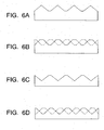
FIG. 6A and FIG. 6C are sectional views of examples of pyramid-shaped projections or recesses formed on a transparent base material film, wherein the projections or recesses are formed to be in a regular lattice shape; and -
FIG. 6B and FIG. 6D are sectional views of examples of pyramid-shaped projections or recesses formed on a transparent base material film, wherein the projections or recesses are formed to be in a hound's-tooth check shape (note that a dotted line indicates pyramid-shaped projections or recesses on the next line). - Note that as to references in the drawings, "a" indicates a length of a side forming a bottom surface of a pyramid shape, "b" indicates a length of other one side forming the bottom surface of the pyramid shape, "c" indicates a height of pyramid-shaped projections or recesses, θ indicates a base angle of side surfaces of the pyramid shape, 1 indicates pyramid-shaped projection or recess, 2 indicates a lens array sheet, and "s" indicates a width between pyramid shaped projections or recesses.
- Below, the present invention will be explained based on embodiments shown in drawings.
- A lens array sheet has pyramid-shaped projections or recesses on a surface (preferably, on one surface) of a transparent base material film.
- A transparent base material film to be used in the present invention is a film shaped mold composed substantially of a transparent resin material. The expression "composed substantially of a transparent resin material" means the case of composing all by a transparent resin material and the case of including various additives in accordance with need as far as it is not more than 50 wt% or so with respect to the total amount.
- As specific examples of the transparent resin material, polyethylene, polypropylene, polymethylpentene and other linear polyolefin resins; polystyrene and other aromatic vinyl based resins; a norbornene based polymer, a vinyl alicyclic hydrocarbon polymer, a monocyclic olefin based polymer, a cyclic diolefin based polymer and other alicyclic olefin resins; polycarbonate, polyethylene phthalate, polybutylene phthalate, liquid crystal polyester and other polyester based resins; polymethyl methacrylate and other acrylic resins; an acrylonitrile styrene resin, an acrylonitrile styrene butadiene resin and other acrylonitrile based resins; polysulfone, polyether sulfone, polyphenylene sulfide, polyphenylene ether and other polyether based resins; and polyether ether ketone and other ketone based resins; may be mentioned.
- Among them, a linear polyolefin resin, an alicyclic olefin resin and polyether based resin, etc. are preferable because they easily bring cross-linking reaction by irradiation of an active energy beam and solubility in specific solvents easily changes. Furthermore, an alicyclic olefin resin is the most preferable because of less absorption of visible light and a low water-absorbing property.
- As specific examples of an alicyclic olefin resin, a ring-opened polymer of a norbornene based monomer and the hydrogenated product, a ring-opened polymer of other monomer capable of copolymerizing with a norbornene based monomer and the hydrogenated product, an addition polymer of a norbornene based monomer and the hydrogenated product, an additional copolymer with other monomer capable of copolymerizing with a norbornene based monomer and the hydrogenated product and other norbornene based polymers; polyvinylcycloalkane, polyvinylcycloalkene, hydrogenated product of an aromatic vinyl polymer and other vinyl alicyclic hydrocarbon polymer; polycyclopentene, polycyclohexene and other monocyclic olefin based polymers; polycyclohexadiene and other cyclic diolefin based polymers; etc. may be mentioned. Among them, a norbornene based polymer and a vinyl alicyclic hydrocarbon polymer are the most preferable. Also, a vinyl alicyclic hydrocarbon polymer may be a copolymer with other monomer (for example, butadiene, isoprene and other vinyl based monomers, etc.) capable of copolymerizing with vinylcycloalkane, vinylcycloalkene and an aromatic vinyl based monomer, etc., and the polymer form may be either of a block polymer and a random polymer.
- A thickness of the transparent base material film is normally 0.05 to 3 mm or so.
- Projections or recesses on a surface of the transparent base material are pyramid shaped.
- The projections or recesses may have a pyramid shape having different base angles of side surfaces or a right pyramid shape wherein all of the bottom angles are the same. Alternately, it may be a pyramid shape wherein an apex angle is cut off. Specifically, shapes shown in
FIG. 1A, FIG. 1B ,FIG. 2A, FIG. 2B ,FIG. 3A, FIG. 3B ,FIG. 4A and FIG. 4B are the examples but it is not limited to these. - Also, in terms of improving front luminance by improving the light condensing property, it is preferable that the bottom surface of the pyramid shape is a rectangular or square shape satisfying the relationship below. The relationship is preferably (length "a" of one side) ≤ (length "b" of other side) ≤ 10a, more preferably (length "a" of one side) ≤ (length "b" of other side) ≤ 5a, further preferably (length "a" of one side) ≤ (length "b" of other side) ≤ 2a, particularly preferably (length "a" of one side) ≤ (length "b" of other side) ≤ 1.5a.
- The length "a" of one side of the bottom surface of the pyramid shape is not particularly limited but is normally 0.1 µm to 500 µm, preferably 0.1 µm to 100 µm. Particularly in the case of obtaining an organic electroluminescence element by using a lens array sheet of the present invention as a light condensing plate and using it as a backlight of a liquid crystal display device, the length "a" is preferably 0.1 µm to 20 µm, so that the liquid crystal is capable of preventing interference by an outside light (so-called moiré).
- The base angle θ of side surfaces of the pyramid shape is preferably 20° to 80°, particularly preferably 30° to 75°.
- A height "c" of the pyramid shape (a length from the bottom surface to the apex angle) is not particularly limited and is preferably 0.2a ≤ c ≤ 2a, more preferably 0.5a ≤ c ≤ 1.5a with respect to the length "a" of one side of the bottom surface of the pyramid shape.
- It is sufficient when a large number of the projections and recesses as above are arranged on a surface of a transparent base material film, and directions of the respective projections and recesses may be a regular lattice shape as shown in
FIG. 5A , a hound's-tooth check shape as shown inFIG. 5B , or a random shape as shown inFIG. 5C . A regular lattice shape or hound's-tooth check shape is preferable for obtaining higher luminance. - Also, a shape of the respective projections or recesses arranged on the surface of the transparent base material film may be all same or independent shapes from one another.
- A method of forming pyramid-shaped projections or recesses on a surface of the transparent base material film is not particularly limited. As typical techniques, for example, (1) a method of setting a mold formed with pyramid-shaped projections or recesses to perform injection molding, compression molding or heat-melt molding, such as blow molding, (2) a method of using a die formed with pyramid-shaped projections or recesses to perform melt extrusion molding, (3) a so-called 2P method for applying an ultraviolet ray curing resin on a molding surface formed with pyramid-shaped projections or recesses, then, curing the resin by irradiating an ultraviolet ray to transfer a pattern, may be mentioned. Among them, a method of transferring a pattern by using the above method (1) is preferable.
- A method of producing a mold is not particularly limited. For example, to produce a mold having pyramid-shaped "projections" on its surface, a method of forming a metal layer by stacking a metal by a soldering method or a sputtering method, etc. on a substrate formed with a pyramid-shaped concave pattern, then, peeling the metal layer from the substrate may be mentioned.
- To obtain a mold having pyramid-shaped "recesses" on its surface, a method of using a mold having pyramid-shaped projections obtained as above and performing mold release processing for bringing the mold surface into contact with potassium bichromate or other oxidizing agent, etc. in accordance with need, then, forming a metal layer by the same method as above by stacking metal, and peeling the metal layer from the mold may be mentioned.
- A method of obtaining a substrate formed with a pyramid-shaped concave pattern is not particularly limited, and a method of using a property that a silicon single crystal substrate is anisotropically etched by an alkaline solution (etching solution) may be mentioned as a preferable example because a fine pattern is easily obtained. Specifically, this method is by (1) stacking an oxidized silicon film and a photo resist film on a silicon substrate in this order, then, forming a pattern on the photoresist film, (2) performing etching on the oxidized silicon layer by an etching solution containing hydrofluoric acid by using the resist pattern as a mask to form a silicon oxide pattern, (3) furthermore, performing anisotropic etching on the silicon substrate by a sodium hydroxide solution or other alkaline etching solution to form pyramid-shaped recesses on the silicon substrate (at this time, the resist pattern can be also removed at a time for it is soluble in the alkaline etching solution), and (4) bringing the finally left silicon oxide pattern into contact with an etching solution containing hydrofluoric acid to remove the silicon oxide pattern, projection or recesses (pattern) is formed on the surface of the silicon substrate.
- When forming pyramid-shaped projections or recesses on a surface of a transparent base material film by using a mold produced by the above explained method, a width of a resist pattern to be a mask becomes a width "s" between adjacent projections or recesses on a lens array sheet of the present invention. The narrower the width "s" is, the more preferable. It is preferably 50% or less, more preferably 20% or less, further preferably 10% or less and particularly preferably 5% or less with respect to a length "a" of one side of the bottom surface of the pyramid shape.
- A light condensing plate is made by the above lens array sheet.
- An organic electroluminescence element of the present invention is obtained by stacking a transparent electrode layer, such as indium tin oxide (ITO), an organic electroluminescence material layer including an organic element, and a metal electrode layer in this order on the lens array sheet as a transparent substrate. In the organic electroluminescence element, the lens array sheet functions as a light condensing plate.
- The organic electroluminescence element can be used as a backlight of a liquid crystal display device, etc.
- Next, specific examples will be taken to explain the present invention more in detail.
- After applying a positive type photoresist composition (product name: ZPP1700PG) made by ZEON Corporation by spin-coating on a substrate obtained by forming a film of SiO2 to 300Å on a silicon, the result was prebaked at 100°C to obtain a resist film of 1.5 µm on the substrate.
- The obtained resist film was subjected to exposure of 50 mJ/cm2 by an exposure apparatus "PLA501F" made by Canon Inc. via a mask, development processing was performed by a 2.38% tetramethyl ammonium hydroxide solution for 60 seconds, and then, rinse processing by ultrapure water was performed for 30 seconds. The substrate was dried by spin processing and prebaking processing at 120°C was finally performed to obtain a resist pattern on the substrate.
- The thus obtained substrate was dipped in a hydrofluoric acid buffer solution (mixture of 3.6% hydrofluoric hydrofluoric water and 18% hydrofluoric ammonium water by 1:1 (in volume) at 20°C. It will be the same below.) for five minutes to etch SiO2, rinsing processing for immersing the etched substrate in pure water for 60 seconds was performed, then, the substrate was dried by spin processing.
- The substrate, wherein the oxide silicon film was etched, was immersed in a 30% sodium hydroxide solution for 30 minutes at 80°, immersed in pure water for 60 seconds, then, dried by blowing a dry air, so that pyramid-shaped concave recesses were formed on the silicon substrate.
- To remove an excessive oxide silicon film remaining on the silicon substrate formed with the recesses, the substrate was dipped in a hydrofluoric acid buffer solution for 5 minutes, then, immersed in pure water for 60 seconds, and dried by blowing a dry air, so that a silicon substrate having pyramid-shaped recesses was produced.
- After adhering the obtained silicon substrate on a fixture and forming a nickel film of about 500Å by vacuum evaporation on the surface, nickel metal was grown by performing electrolytic soldering in an electrolytic solution containing nickel sulfamate as its main component. The obtained nickel block (metal layer) was peeled from the silicon substrate, so that a mold (convex mold) formed with pyramid-shaped "'projections" in a hound's-tooth check shape was produced.
- This mold was set in an injection molding apparatus to obtain a lens array sheet (the outside dimension is 40 mm × 40 mm) having a thickness of about 1 mm by injection molding (resin melt temperature of 285°C, mold temperature of 130°C, and resin filling time of about 0.2 second) using a cycloolefin polymer (ZNR1430R made by ZEON Corporation).
- The obtained lens array sheet was formed on its surface with pyramid-shaped "recesses" having a bottom surface of 20 µm × 20 µm, a base angle of side surfaces of approximately 55° and a height of 14 µm in a hound's-tooth check shape.
- ITO having a thickness of 300Å was evaporated on the thus obtained lens array sheet, the result was washed with steam of IPA, set in an organic electroluminescence element producing apparatus, and subjected to plasma processing at 100W under an atmosphere of oxygen/argon = 50/50 for 5 minutes.
- After that, the result was transferred to an organic evaporation chamber, and N,N-di(1-naphthyl)-N,N'-diphenyl-1,1'-diphenyl-1,4-imine (NPD) as a hole transport material and 8-hydroxy quinoline aluminum (Alq3) as an electron transport material were put in two melting pots wound by coil. Then, inside the chamber was depressurized to 10-6 Pa and a current of 20A was applied to the coil holding NPD to perform evaporation until the film thickness becomes 400Å, then, evaporation was performed under the same condition until a film thickness of Alq3 becomes 600Å, so that an organic electroluminescence material layer was stacked.
- After that, the substrate was moved to a metal evaporation chamber while keeping in the system in a vacuum state, and lithium fluoride loaded on a metal board was heated, so that the lithium fluoride was evaporated to be 5Å on the organic layer. Then, aluminum was loaded on another metal board to evaporate it to be a thickness of 1000Å by the same operation, so that a stacked body, wherein an ITO layer, an organic electroluminescence material layer and a metal electrode layer were stacked, was obtained on the lens array sheet.
- The thus obtained stacked body was attached with a stainless sealing tube applied with an ultraviolet ray curing adhesion in a globe box in a dry nitrogen, and an ultraviolet ray was irradiated to adhere the sealing tube, consequently, an organic electroluminescence element was obtained.
- Measurement of luminance was made on the obtained element by a luminance measurement device (BM-8 made by TOPCON CORPORATION) in a state of being placed vertical with respect to the substrate surface, and the result was 2165 cd/cm2. When luminance was measured in the same way in a state of giving a tilt by 45° with respect to the substrate surface respectively to above, below, right and left (evaluation of a viewable angle), the result was above: 2100 cd/cm2, below: 2120 cd/cm2, left: 2135 cd/cm2 and right 2140 cd/cm2. Namely, sufficient luminance was obtained even when viewing from the directions tilted by 45° with respect to the substrate surface, so that it was confirmed that a sufficient viewable angle was attained.
- Other than using a film of a cycloolefin polymer (ZNR1430R made by ZEON Corporation) having a thickness of 1 mm and not formed with concaves and convexes instead of the lens array sheet of the example 1, an organic electroluminescence element was produced in the same method as in the example 1, and the luminance was measured under the same condition. The result was 1250 cd/cm2. Accordingly, it was confirmed that by using the lens array sheet of the example 1 as a light condensing plate, luminance of the organic electroluminescence element was improved to about 1.5 times.
- Also, evaluation of the viewable angle measured in the same way was above: 1000 cd/cm2, below: 955 cd/cm2, left: 990 cd/cm2 and right 930 cd/cm2.
- The mold in the example 1 was used. The mold was immersed in a potassium bichromate solution (0.1 wt%) for 30 seconds and mold releasing processing was performed by oxidizing the mold surface, then, a nickel layer (metal layer) was stacked under the same condition as that in the example 1 and the stacked nickel layer was peeled from the mold, so that a mold (concave mold) formed with pyramid-shaped "recesses" having a base angle of side surfaces of approximately 55° and a height of 14 µm in a hound's-tooth check shape was obtained.
- By using the obtained mold, a lens array sheet was produced in the same way as in the example 1. The obtained lens array sheet was formed on its surface with pyramid-shaped "projections" having a bottom surface of 20 µm ×20 µm, a base angle of side surfaces of approximately 55° and a height of 14 µm in a hound's-tooth check shape.
- By using the lens array sheet, an organic electroluminescence element was produced, and the luminance was measured under the same condition. The result was 1420 cd/cm2. From the result, it was confirmed that luminance of the organic electroluminescence element was improved to about 1.7 times comparing with that in the comparative example 1 by using the lens array sheet of the example 2 as a light condensing plate.
- Also, evaluation of the viewable angle measured in the same way was above: 1400 cd/cm2, below: 1395 cd/cm2, left: 1405 cd/cm2 and right 1380 cd/cm2, and superiority of the example 2 to the comparative example 1 was confirmed.
- The followings are understood from the examples 1, 2 and the comparative example 1 above. When using as a light condensing plate a lens array sheet formed with a plurality of projections or recesses on one surface of a transparent base material film, luminance of an organic electroluminescence element improves. Particularly, by choosing "recesses" from the projections and recesses to form, higher luminance is obtained.
- A viewing angle was confirmed to have a tendency of becoming wider as the luminance improves.
- A lens array sheet exhibits remarkable efficiency in improving luminance as a light condensing plate of an organic electroluminescence element.
- The lens array sheet can be used as an optical part, such as an information recording medium, optical lens, optical filter, light guide plate for a liquid crystal display device and optical sheet, in addition to being used as a light condensing plate of an organic electroluminescence element.
Claims (8)
- An organic electroluminescence element, comprising
a transparent substrate composed of a lens array sheet (2) having a plurality of recesses (1) on a surface of its transparent base material film,
a transparent electrode layer stacked on the transparent substrate,
an organic electroluminescence material layer stacked on the transparent electrode layer, and a metal electrode layer stacked on the organic electroluminescence material layer, characterized in that the recesses are pyramid shaped and
wherein the shape of the bottom surface of the pyramid is a rectangular or square shape satisfying a relationship of (length "a" of one side) ≤ (length "b" of other side) ≤ 10a,
and wherein adjacent pyramid shaped recesses are separated from adjacent pyramid shaped recesses and the width "s" between adjacent pyramid shaped recesses is not more than 50% of the length "a". - The organic electroluminescence element as set forth in claim 1, wherein the length "a" of one side of the bottom surface of the pyramid shape is 0.1 µm to 20 µm.
- The organic electroluminescence element as set forth in claim 2, wherein a height "c" of the pyramid shape is 0.2a ≤ c ≤ 2a with respect to the length "a".
- The organic electroluminescence element as set forth in claim 1, wherein a base angle θ of side surfaces of the pyramid shape is 20° to 80°.
- The organic electroluminescence element as set forth in claim 1, wherein the transparent base material film is composed substantially of an alicyclic olefin resin.
- The organic electroluminescence element as set forth in claim 5, wherein the alicyclic olefin resin is a norbornene based polymer or a vinyl alicyclic hydrocarbon polymer.
- A process for the production of the organic electroluminescence element as set forth in claim 1, comprising the formation of a lens array sheet as defined in this claim by injection molding using a mold made by a metal layer and provided with pyramid shaped projections on its surface, wherein said metal layer is obtained by forming a metal layer on a substrate formed with a pyramid-shaped concave pattern and peeling the metal layer from the substrate, and
wherein as the substrate formed with a pyramid-shaped concave pattern, a mold made by silicon formed by(1) a step of forming a positive type resist pattern on a silicon wafer formed on its surface with a silicon oxide layer,(2) a step of forming a silicon oxide pattern by performing etching on the silicon oxide layer by an etching solution containing hydrofluoric acid by using the resist pattern as a mask,(3) a step of removing the resist pattern and performing anisotropic etching on the silicon wafer surface by an alkaline solution to form pyramid-shaped recesses, and(4) a step of removing the silicon oxide pattern by an etching solution containing hydrofluoric acid is used. - A display device comprising an organic electroluminescence element as set forth in claim 1.
Applications Claiming Priority (3)
| Application Number | Priority Date | Filing Date | Title |
|---|---|---|---|
| JP2002236040 | 2002-08-13 | ||
| JP2002236040 | 2002-08-13 | ||
| PCT/JP2003/010255 WO2004017106A1 (en) | 2002-08-13 | 2003-08-12 | Lens array sheet |
Publications (3)
| Publication Number | Publication Date |
|---|---|
| EP1548470A1 EP1548470A1 (en) | 2005-06-29 |
| EP1548470A4 EP1548470A4 (en) | 2008-03-12 |
| EP1548470B1 true EP1548470B1 (en) | 2014-02-12 |
Family
ID=31884394
Family Applications (1)
| Application Number | Title | Priority Date | Filing Date |
|---|---|---|---|
| EP03788087.9A Expired - Lifetime EP1548470B1 (en) | 2002-08-13 | 2003-08-12 | Organic electroluminescence element comprising a lens array sheet |
Country Status (6)
| Country | Link |
|---|---|
| US (1) | US7710031B2 (en) |
| EP (1) | EP1548470B1 (en) |
| JP (1) | JP4507880B2 (en) |
| KR (1) | KR100992222B1 (en) |
| CN (1) | CN100462739C (en) |
| WO (1) | WO2004017106A1 (en) |
Families Citing this family (35)
| Publication number | Priority date | Publication date | Assignee | Title |
|---|---|---|---|---|
| JP2005055481A (en) * | 2003-06-09 | 2005-03-03 | Toyota Industries Corp | Optical element, planar illumination device, and display device |
| JP4707085B2 (en) * | 2004-03-01 | 2011-06-22 | アーベル・システムズ株式会社 | LCD display |
| CN100576587C (en) | 2005-04-13 | 2009-12-30 | 皇家飞利浦电子股份有限公司 | Structured Substrates for LEDs |
| JP2006330723A (en) * | 2005-05-20 | 2006-12-07 | Samsung Electronics Co Ltd | Optical plate, backlight assembly having the same, and display device |
| DE102005027799B4 (en) | 2005-06-16 | 2007-09-27 | Saint-Gobain Glass Deutschland Gmbh | Method for producing a transparent pane with a surface structure and apparatus for carrying out the method |
| US20080032096A1 (en) * | 2006-08-07 | 2008-02-07 | Eastman Kodak Company | Microstructured film containing polysulfone polymer |
| JPWO2008023586A1 (en) * | 2006-08-23 | 2010-01-07 | 日本ゼオン株式会社 | Electroluminescence element, lighting device, and liquid crystal display device |
| JPWO2009016991A1 (en) * | 2007-08-01 | 2010-10-14 | コニカミノルタオプト株式会社 | Injection molding apparatus, molding method, molded product, and optical element |
| CN102066456A (en) | 2008-06-20 | 2011-05-18 | 3M创新有限公司 | Molded microstructured articles and methods of making the same |
| US8829784B2 (en) * | 2009-06-11 | 2014-09-09 | Zeon Corporation | Surface light source device, lighting device, and backlight device |
| WO2012086623A1 (en) | 2010-12-24 | 2012-06-28 | 日本ゼオン株式会社 | Light emitting element |
| EP2479015A1 (en) * | 2011-01-19 | 2012-07-25 | Moser Baer India Ltd. | Method of molding structures in plastic substrate |
| CN102683607B (en) * | 2011-03-14 | 2015-01-07 | 海洋王照明科技股份有限公司 | Organic electroluminescent device and preparation method thereof |
| US9112182B2 (en) | 2011-03-29 | 2015-08-18 | Zeon Corporation | Light-emitting element and illuminating apparatus |
| KR101871538B1 (en) * | 2011-04-27 | 2018-06-26 | 제이엑스티지 에네루기 가부시키가이샤 | Light extraction transparent substrate for organic electroluminescent element and organic electroluminescent element using same |
| JP5664453B2 (en) * | 2011-05-18 | 2015-02-04 | コニカミノルタ株式会社 | Light emitting element |
| JP2012243494A (en) * | 2011-05-18 | 2012-12-10 | Konica Minolta Holdings Inc | Light emitting element |
| JP5803506B2 (en) | 2011-09-28 | 2015-11-04 | 日本ゼオン株式会社 | Light emitting device and lighting apparatus |
| JP6053692B2 (en) | 2011-12-20 | 2016-12-27 | キヤノン株式会社 | Data transfer device, data transfer method, and inter-chip communication system |
| RU2551127C1 (en) * | 2013-11-07 | 2015-05-20 | Алексей Николаевич Миронов | Lamp and optical element therefor |
| USD780704S1 (en) * | 2014-08-27 | 2017-03-07 | Mitsubishi Electric Corporation | Light source module |
| USD768584S1 (en) * | 2014-11-13 | 2016-10-11 | Mitsubishi Electric Corporation | Light source module |
| WO2016178592A1 (en) * | 2015-05-05 | 2016-11-10 | Алексей Николаевич МИРОНОВ | Lamp and optical element for same |
| CN104808267A (en) * | 2015-05-08 | 2015-07-29 | 南昌航空大学 | OLED (organic light emitting diode) illuminating light extraction membrane |
| CN104849797A (en) * | 2015-05-28 | 2015-08-19 | 张家港康得新光电材料有限公司 | Guide film and LED display screen with application of guide film |
| CN105068298B (en) * | 2015-06-23 | 2018-01-12 | 深圳市华星光电技术有限公司 | Visual angle expands film and includes its wide viewing angle thin-film transistor LCD device |
| CN106324754B (en) * | 2016-11-14 | 2019-07-16 | 四川大学 | Optical devices and unidirectional guided wave structures |
| CN111656614B (en) | 2018-02-06 | 2021-10-15 | 华为技术有限公司 | Lenses, lens antennas, remote radio units and base stations |
| CN110161613B (en) * | 2018-03-30 | 2020-12-08 | 京东方科技集团股份有限公司 | Backlight module and its manufacturing method, liquid crystal display device |
| KR102221188B1 (en) * | 2019-03-14 | 2021-03-03 | 주식회사 엘엠에스 | Backlight unit using mini led or micro led as light source |
| CN111435205A (en) * | 2019-06-28 | 2020-07-21 | 宁波激智科技股份有限公司 | Novel rectangular pyramid brightness enhancement film and preparation method thereof |
| CN115576132B (en) * | 2020-03-13 | 2024-03-19 | 大日本印刷株式会社 | Display device and method for manufacturing optical film |
| CN116113857A (en) * | 2020-09-15 | 2023-05-12 | 大日本印刷株式会社 | Optical film and display device |
| KR102471143B1 (en) * | 2022-04-29 | 2022-11-29 | 주식회사 멤스룩스 | Lighting glasses |
| CN117518589A (en) * | 2023-01-31 | 2024-02-06 | 武汉华星光电技术有限公司 | A kind of backlight module and display panel |
Citations (1)
| Publication number | Priority date | Publication date | Assignee | Title |
|---|---|---|---|---|
| WO2003046617A1 (en) * | 2001-11-28 | 2003-06-05 | Saint-Gobain Glass France | Textured transparent plate with high light transmission |
Family Cites Families (35)
| Publication number | Priority date | Publication date | Assignee | Title |
|---|---|---|---|---|
| JPS55138602U (en) * | 1979-03-26 | 1980-10-02 | ||
| JPH06308485A (en) * | 1993-04-21 | 1994-11-04 | Hitachi Ltd | Display device |
| JPH078805A (en) | 1993-06-23 | 1995-01-13 | Japan Gore Tex Inc | Metal-containing catalyst and catalytic reactor |
| JPH078805U (en) * | 1993-06-29 | 1995-02-07 | 第二しなのポリマー株式会社 | Directional diffuser and its applications |
| JPH07114025A (en) | 1993-10-20 | 1995-05-02 | Sharp Corp | Liquid crystal display |
| JPH07318918A (en) | 1994-05-27 | 1995-12-08 | Alps Electric Co Ltd | Distributed display device and prism film |
| JPH08271888A (en) | 1995-03-29 | 1996-10-18 | Sumitomo Bakelite Co Ltd | Light control sheet for liquid crystal display |
| JPH08278413A (en) * | 1995-04-04 | 1996-10-22 | Dainippon Printing Co Ltd | Surface light source device and manufacturing method thereof |
| JPH0968605A (en) | 1995-06-20 | 1997-03-11 | Nippon Kayaku Co Ltd | Condensing lens sheet, light source device using the same, and liquid crystal display device |
| US5714218A (en) * | 1995-08-21 | 1998-02-03 | Dainippon Printing Co., Ltd. | Ionizing radiation-curable resin composition for optical article, optical article, and surface light source |
| JP3277101B2 (en) * | 1995-09-04 | 2002-04-22 | 東洋インキ製造株式会社 | Coloring composition for color filter and color filter |
| JPH09326297A (en) | 1996-06-04 | 1997-12-16 | Casio Comput Co Ltd | EL device |
| JPH09323354A (en) | 1996-06-05 | 1997-12-16 | Japan Synthetic Rubber Co Ltd | Optical sheet |
| US6447879B1 (en) * | 1996-09-17 | 2002-09-10 | Kabushiki Kaisha Toshiba | Electronic Device and method of manufacturing the same |
| JPH10125123A (en) * | 1996-10-22 | 1998-05-15 | Matsushita Electric Ind Co Ltd | Backlight |
| JP3938253B2 (en) * | 1997-12-26 | 2007-06-27 | 日本板硝子株式会社 | Resin erecting equal-magnification lens array and manufacturing method thereof |
| JP4286923B2 (en) * | 1998-01-13 | 2009-07-01 | 大日本印刷株式会社 | Liquid crystal display |
| JPH11326603A (en) * | 1998-05-19 | 1999-11-26 | Seiko Epson Corp | Microlens array, method of manufacturing the same, and display device |
| ITTO980580A1 (en) | 1998-07-02 | 2000-01-02 | C R F Societa Consotile Per Az | LIGHT EMITTER DEVICE, BASED ON ELECTRO-LUMINESCENT ORGANIC MATERIAL, WITH COMPLIANT EXTERNAL INTERFACE |
| JP2000068069A (en) * | 1998-08-13 | 2000-03-03 | Idemitsu Kosan Co Ltd | Organic electroluminescence device and method of manufacturing the same |
| JP2000075102A (en) | 1998-08-31 | 2000-03-14 | Nippon Zeon Co Ltd | Condensing sheet |
| JP4198246B2 (en) * | 1998-11-16 | 2008-12-17 | 株式会社クラレ | Surface light source element |
| JP2000292790A (en) * | 1999-02-04 | 2000-10-20 | Keiwa Inc | Light diffusion sheet and backlight unit using the same |
| JP2000263556A (en) * | 1999-03-18 | 2000-09-26 | Canon Inc | Method for producing microlens mold and method for producing microlens using the same |
| JP3654059B2 (en) * | 1999-06-25 | 2005-06-02 | 松下電工株式会社 | Infrared sensor manufacturing method |
| US6421104B1 (en) * | 1999-10-22 | 2002-07-16 | Motorola, Inc. | Front illuminator for a liquid crystal display and method of making same |
| JP2001208903A (en) | 2000-01-26 | 2001-08-03 | Nakane:Kk | Light collecting film |
| US6777871B2 (en) * | 2000-03-31 | 2004-08-17 | General Electric Company | Organic electroluminescent devices with enhanced light extraction |
| JP2002122706A (en) * | 2000-10-12 | 2002-04-26 | Ngk Insulators Ltd | Micro lens array and method of manufacturing the same |
| JP3815221B2 (en) | 2001-01-11 | 2006-08-30 | セイコーエプソン株式会社 | LIGHTING DEVICE, DISPLAY DEVICE, AND ELECTRONIC DEVICE |
| TW589913B (en) * | 2001-01-18 | 2004-06-01 | Ind Tech Res Inst | Organic light-emitting device |
| US6984934B2 (en) | 2001-07-10 | 2006-01-10 | The Trustees Of Princeton University | Micro-lens arrays for display intensity enhancement |
| JP3828402B2 (en) * | 2001-11-08 | 2006-10-04 | 株式会社日立製作所 | BACKLIGHTING DEVICE, LIQUID CRYSTAL DISPLAY DEVICE USING SAME, AND LIGHTING METHOD FOR LIQUID CRYSTAL DISPLAY DEVICE |
| US7011420B2 (en) * | 2002-09-04 | 2006-03-14 | Eastman Kodak Company | Planar directed light source |
| US6997595B2 (en) * | 2003-08-18 | 2006-02-14 | Eastman Kodak Company | Brightness enhancement article having trapezoidal prism surface |
-
2003
- 2003-08-12 KR KR1020057002391A patent/KR100992222B1/en not_active Expired - Fee Related
- 2003-08-12 WO PCT/JP2003/010255 patent/WO2004017106A1/en not_active Ceased
- 2003-08-12 CN CNB038236397A patent/CN100462739C/en not_active Expired - Fee Related
- 2003-08-12 US US10/524,117 patent/US7710031B2/en not_active Expired - Fee Related
- 2003-08-12 JP JP2004528863A patent/JP4507880B2/en not_active Expired - Fee Related
- 2003-08-12 EP EP03788087.9A patent/EP1548470B1/en not_active Expired - Lifetime
Patent Citations (1)
| Publication number | Priority date | Publication date | Assignee | Title |
|---|---|---|---|---|
| WO2003046617A1 (en) * | 2001-11-28 | 2003-06-05 | Saint-Gobain Glass France | Textured transparent plate with high light transmission |
Also Published As
| Publication number | Publication date |
|---|---|
| KR100992222B1 (en) | 2010-11-05 |
| US7710031B2 (en) | 2010-05-04 |
| US20050212989A1 (en) | 2005-09-29 |
| WO2004017106A1 (en) | 2004-02-26 |
| JP4507880B2 (en) | 2010-07-21 |
| EP1548470A1 (en) | 2005-06-29 |
| JPWO2004017106A1 (en) | 2005-12-08 |
| CN1688901A (en) | 2005-10-26 |
| EP1548470A4 (en) | 2008-03-12 |
| CN100462739C (en) | 2009-02-18 |
| KR20050053610A (en) | 2005-06-08 |
Similar Documents
| Publication | Publication Date | Title |
|---|---|---|
| US7710031B2 (en) | Lens array sheet | |
| US8097479B2 (en) | Anti-reflective film and production method thereof, and stamper for producing anti-reflective film and production method thereof | |
| US7692860B2 (en) | Wire grid polarizer and method of manufacturing the same | |
| CN100431196C (en) | Forming Electrode Patterns in Organic Light Emitting Diode Devices | |
| US20040174596A1 (en) | Polarization optical device and manufacturing method therefor | |
| US20240085589A1 (en) | Optical elements including a metastructure having cone-shaped or truncated cone-shaped meta-atoms and its manufacturing method | |
| KR20250117364A (en) | Display panel and manufacturing method thereof, display device | |
| JP3956190B2 (en) | Ferroelectric capacitor array and method for manufacturing ferroelectric memory | |
| CN1735171A (en) | Method of manufacturing substrate having recessed portions for microlenses and transmissive screen | |
| JPWO2011078254A1 (en) | Absorption-type polarizing element and manufacturing method thereof | |
| WO2006067368A1 (en) | Organic electroluminescent device | |
| JP2010266551A (en) | LCD lens | |
| JP2004271558A (en) | Polarizing optical element and its manufacturing method | |
| JP2012216084A (en) | Information input device | |
| KR20030019241A (en) | Stamper, manufacturing method therefor and optical device manufactured therewith | |
| US20070171529A1 (en) | Method for manufacturing optical element | |
| US6922227B2 (en) | Plastic liquid crystal display device and method for manufacturing the same | |
| JP2001247339A (en) | Method for manufacturing microlens array and method for manufacturing electro-optical device | |
| CN100373655C (en) | Organic light emitting display and method of manufacturing the same | |
| TWI824679B (en) | Display device and method for fabricating the same | |
| CN220897089U (en) | Pixel defining structure and display panel | |
| KR20050081361A (en) | Film of light scattering, method for manufacturing the same, and display device | |
| KR100462045B1 (en) | An metal cap for encapsulating an organic electro-luminescence device and a fabricating method thereof | |
| GB2421626A (en) | Organic electroluminescent device | |
| KR20210007407A (en) | Transparent electrode laminate and method of manufacturing the same |
Legal Events
| Date | Code | Title | Description |
|---|---|---|---|
| PUAI | Public reference made under article 153(3) epc to a published international application that has entered the european phase |
Free format text: ORIGINAL CODE: 0009012 |
|
| 17P | Request for examination filed |
Effective date: 20050225 |
|
| AK | Designated contracting states |
Kind code of ref document: A1 Designated state(s): AT BE BG CH CY CZ DE DK EE ES FI FR GB GR HU IE IT LI LU MC NL PT RO SE SI SK TR |
|
| RBV | Designated contracting states (corrected) |
Designated state(s): DE FR GB NL |
|
| A4 | Supplementary search report drawn up and despatched |
Effective date: 20080213 |
|
| 17Q | First examination report despatched |
Effective date: 20090710 |
|
| GRAP | Despatch of communication of intention to grant a patent |
Free format text: ORIGINAL CODE: EPIDOSNIGR1 |
|
| INTG | Intention to grant announced |
Effective date: 20131001 |
|
| GRAS | Grant fee paid |
Free format text: ORIGINAL CODE: EPIDOSNIGR3 |
|
| GRAA | (expected) grant |
Free format text: ORIGINAL CODE: 0009210 |
|
| AK | Designated contracting states |
Kind code of ref document: B1 Designated state(s): DE FR GB NL |
|
| REG | Reference to a national code |
Ref country code: GB Ref legal event code: FG4D |
|
| REG | Reference to a national code |
Ref country code: DE Ref legal event code: R096 Ref document number: 60345709 Country of ref document: DE Effective date: 20140320 |
|
| REG | Reference to a national code |
Ref country code: NL Ref legal event code: VDEP Effective date: 20140212 |
|
| PG25 | Lapsed in a contracting state [announced via postgrant information from national office to epo] |
Ref country code: NL Free format text: LAPSE BECAUSE OF FAILURE TO SUBMIT A TRANSLATION OF THE DESCRIPTION OR TO PAY THE FEE WITHIN THE PRESCRIBED TIME-LIMIT Effective date: 20140212 |
|
| REG | Reference to a national code |
Ref country code: DE Ref legal event code: R097 Ref document number: 60345709 Country of ref document: DE |
|
| PLBE | No opposition filed within time limit |
Free format text: ORIGINAL CODE: 0009261 |
|
| STAA | Information on the status of an ep patent application or granted ep patent |
Free format text: STATUS: NO OPPOSITION FILED WITHIN TIME LIMIT |
|
| 26N | No opposition filed |
Effective date: 20141113 |
|
| REG | Reference to a national code |
Ref country code: DE Ref legal event code: R097 Ref document number: 60345709 Country of ref document: DE Effective date: 20141113 |
|
| REG | Reference to a national code |
Ref country code: FR Ref legal event code: PLFP Year of fee payment: 14 |
|
| REG | Reference to a national code |
Ref country code: FR Ref legal event code: PLFP Year of fee payment: 15 |
|
| REG | Reference to a national code |
Ref country code: FR Ref legal event code: PLFP Year of fee payment: 16 |
|
| PGFP | Annual fee paid to national office [announced via postgrant information from national office to epo] |
Ref country code: FR Payment date: 20180712 Year of fee payment: 16 Ref country code: DE Payment date: 20180731 Year of fee payment: 16 |
|
| PGFP | Annual fee paid to national office [announced via postgrant information from national office to epo] |
Ref country code: GB Payment date: 20180808 Year of fee payment: 16 |
|
| REG | Reference to a national code |
Ref country code: DE Ref legal event code: R119 Ref document number: 60345709 Country of ref document: DE |
|
| GBPC | Gb: european patent ceased through non-payment of renewal fee |
Effective date: 20190812 |
|
| PG25 | Lapsed in a contracting state [announced via postgrant information from national office to epo] |
Ref country code: FR Free format text: LAPSE BECAUSE OF NON-PAYMENT OF DUE FEES Effective date: 20190831 Ref country code: DE Free format text: LAPSE BECAUSE OF NON-PAYMENT OF DUE FEES Effective date: 20200303 |
|
| PG25 | Lapsed in a contracting state [announced via postgrant information from national office to epo] |
Ref country code: GB Free format text: LAPSE BECAUSE OF NON-PAYMENT OF DUE FEES Effective date: 20190812 |