EP1547246B1 - Integrated circuit with automatic polarity detection and configuration - Google Patents
Integrated circuit with automatic polarity detection and configuration Download PDFInfo
- Publication number
- EP1547246B1 EP1547246B1 EP03752479A EP03752479A EP1547246B1 EP 1547246 B1 EP1547246 B1 EP 1547246B1 EP 03752479 A EP03752479 A EP 03752479A EP 03752479 A EP03752479 A EP 03752479A EP 1547246 B1 EP1547246 B1 EP 1547246B1
- Authority
- EP
- European Patent Office
- Prior art keywords
- state
- mute
- node
- output
- input
- Prior art date
- Legal status (The legal status is an assumption and is not a legal conclusion. Google has not performed a legal analysis and makes no representation as to the accuracy of the status listed.)
- Expired - Lifetime
Links
- 238000001514 detection method Methods 0.000 title description 3
- 238000000034 method Methods 0.000 claims description 9
- 230000003213 activating effect Effects 0.000 claims description 2
- 230000008878 coupling Effects 0.000 claims 2
- 238000010168 coupling process Methods 0.000 claims 2
- 238000005859 coupling reaction Methods 0.000 claims 2
- 238000010586 diagram Methods 0.000 description 4
- 239000007795 chemical reaction product Substances 0.000 description 2
- 230000010355 oscillation Effects 0.000 description 1
- 230000000717 retained effect Effects 0.000 description 1
Images



Classifications
-
- H—ELECTRICITY
- H03—ELECTRONIC CIRCUITRY
- H03K—PULSE TECHNIQUE
- H03K19/00—Logic circuits, i.e. having at least two inputs acting on one output; Inverting circuits
-
- H—ELECTRICITY
- H03—ELECTRONIC CIRCUITRY
- H03F—AMPLIFIERS
- H03F3/00—Amplifiers with only discharge tubes or only semiconductor devices as amplifying elements
- H03F3/20—Power amplifiers, e.g. Class B amplifiers, Class C amplifiers
- H03F3/21—Power amplifiers, e.g. Class B amplifiers, Class C amplifiers with semiconductor devices only
- H03F3/217—Class D power amplifiers; Switching amplifiers
- H03F3/2171—Class D power amplifiers; Switching amplifiers with field-effect devices
-
- G—PHYSICS
- G01—MEASURING; TESTING
- G01R—MEASURING ELECTRIC VARIABLES; MEASURING MAGNETIC VARIABLES
- G01R19/00—Arrangements for measuring currents or voltages or for indicating presence or sign thereof
- G01R19/14—Indicating direction of current; Indicating polarity of voltage
Definitions
- the present invention relates generally to the field of integrated circuits and, in particular, to detecting and configuring the required polarity of a circuit pin.
- An integrated circuit or "chip” is generally installed or mounted on a system board which is ultimately installed in an end product.
- an integrated circuit may be purchased for use in several (or many) different end products, often by different manufacturers. It will be appreciated that it may be impractical to use separate chip designs for similar applications. However, in the past, it has also been impractical to automatically modify chips so as to function with a variety of different system boards.
- audio devices such as DVD units and audio/video (A/V) receivers include a digital audio integrated circuit having, among other functional components, a digital-to-analog converter (DAC) for outputting an analog audio reproduction of a digital signal.
- the integrated circuit is mounted on a system board which generally includes a mute circuit to disable the analog audio output during unit power-on, reset or other predetermined events. Absent such mute, the listener would hear clicks and pops which are both distracting to the listener and potentially damaging to the audio device or speakers.
- clicks and pops may still be generated downstream from the DAC, especially as there may be some brief, but finite, time delay after the 0s begin to be input to the DAC.
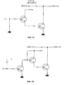
- Figures 1A-1D are examples of mute circuits commonly used on system boards.
- the circuits of Figs. 1A and 1C are activated when the mute signal (actually the inverted mute signal) to the "mute node" is in a low state, driving the mute node to ground; these circuits are said to have an "active low mute”.
- the circuits of Figs. 1B and 1D have an active high mute and are activated when the control signal to the mute node is in a high state.
- the mute circuits is activated by mute driver circuitry on the audio chip which, In turn, is enabled by a mute_control signal 202.
- Fig. 2 is an illustration of a typical prior art mute driver circuit 200.
- transistor M0 is off and M1 is on, driving the mute node 204 high.
- transistor MO is on and M1 is off, driving the mute node 204 low.
- the signal to the mute node 204 must either be high or low.
- the designer of the audio chip must either know In advance with which type of mute circuit the chip will be used and make available the appropriate chip or the system board designer must decide in advance which chip will be used and conform the mute circuit to the chip (and then be limited as to second or future sources of the chip).
- the chip may be designed with configurable polarity.
- configurable polarity requires either an extra and dedicated pin or a register which can be set through a control port whenever the chip goes through a power-on or reset.
- One disadvantage to using a register is that there may still be a delay after the chip exits the reset state until the register is configured. During this time the mute node may be In the unmute state, resulting in the undesirable clicks and pops which were to be eliminated.
- US 5,371,455 discloses a control circuit for safe charging a rechargeable battery, the control circuit comprises a forced short-circuit switch, a safety switch, an automatic change switch, a first rectification circuit, a second rectification circuit, a reverse-polarity detection circuit, a charging-signal output circuit, an oscillation circuit, and a condition-indicating signal assembly.
- Power supply can be provided from a conventional charging device or a spare battery.
- the reverse-polarity detection circuit is used for detecting the correct polarity connection; when reverse polarity is connected, the automatic change switch will correct the polarity by indicating the occurrence of such a condition with the indicating lamps in the condition-indicating signal assembly so as to provide a smooth and safe battery recharging.
- the present invention provides an automatic node polarity detector for use in conjunction with a circuit and a method for activating a circuit on a system board as claimed respectively in independent claim 1 and independent claim 13.
- An embodiment of the present invention provides an integrated circuit mountable on a system board used, for example, in a digital audio device (such as a DVD or A/V receiver).
- the integrated circuit includes a digltal-to-analog converter, possibly in conjunction with a CODEC, and the system board may include circuitry to, for example, mute the analog output of the device under certain predefined conditions.
- the integrated circuit further includes a detector which detects and stores the required polarity (although it will be appreciated that certain of the components of the detector may also be placed off-chip). When it is necessary for the circuit to be activated, the detector provides a signal of the correct polarity.
- Figs. 1A-1D are examples of mute circuits commonly used on system boards
- Fig. 2 is a prior art mute circuit driver
- Fig. 3 is a logic diagram of the present invention incorporated in a mute polarity detector
- Fig. 4 is a logic diagram an alternative embodiment of a mute polarity detector of the present invention.
- Fig. 3 is a high level logic diagram of a polarity detector 300 of the present invention included in an exemplary integrated circuit which also includes a DAC.
- the chip is mountable on a system board having, for example, a mute circuit, preferably of the type illustrated in Figs. 1C or 1D (if a circuit of Figs. 1A or 1 B are used and the input line is left floating, either circuit will self-bias to an undesirable un-muted state).
- a driver circuit 302 is also included on the chip and is similar to the driver circuit illustrated in Fig. 2 . However, rather than the control gates of both switches (such as transistors M0 and M1) being tied to a mute_control signal node as in the prior art of Fig. 2 , they are coupled to separate outputs of the detector 300.
- Inputs to the detector 300 include the mute-control signal 202, a detect_enable signal 304 and a mute_node_status 306 coupled to the mute node 204 (preferably through a buffer 308).
- Outputs include a mute_polarity signal 310 and signals 312 and 314 to the control gates of the switches M0 and M1, respectively.
- a pull-up resistor 326 may be coupled to the mute node 204 such that, if the mute node 204 is disconnected from the mute circuitry, the resistor 326 will prevent the mute node 204 from floating. It will be appreciated that a pull-down resistor may be used instead of the pull-up resistor 326.
- the detector 300 includes an OR gate 316, an AND gate 318, an XOR gate 320, a latch 322 and an inverter 324. It will be appreciated, of course, that any of these logic devices may be replaced by a functional equivalent.
- the mute-control signal 202 is coupled to an input to the XOR gate 320, the detect_enable signal 304 is inverted by the inverter 324 and coupled to an input to the AND gate 318 (alternatively, an inverted detect_enable signal may be generated elsewhere in the chip).
- the detect_enable signal 304 is also coupled to a clock input to the latch 322 and to an input to the OR gate 316.
- the outputs from the AND gate 318 and the OR gate 316 are coupled to the control gates of the switches M0 and M1, respectively.
- the mute_node_status 306 is coupled to the input to the latch 322.
- the mute_polarity signal 310 is coupled to the output of the latch 322.
- the inverted output of the latch 322 is coupled to a second input to the XOR gate 320 whose output is coupled to a second input to the OR gate 316 and to a second input of the AND gate 318.
- the mute_detect signal 304 is asserted (goes to a high state), enabling the latch 322. Simultaneously, the output of the OR gate 316 goes high and the output of the AND gate 318 goes low.
- the switches M0 and M1 thus both turn off, thereby preventing the mute node 204 from being pulled high or low and effectively isolating the mute node 204 from any of the control signals from the detector circuit 300. Consequently, the polarity (or state) of the mute node 204 is determined only by the mute circuitry on the system board and this polarity is detected by the latch 322.
- the mute enable signal 304 is deasserted and the mute polarity is retained in the latch 322.
- the output of the XOR gate 320 will be high if the mute polarity was high and will be low if the mute polarity was low.
- the mute node 204 will thus be pulled high or low as required to properly activate the mute circuitry.
- Fig. 4 is a logic diagram an alternative embodiment of a polarity detector 400 of the present invention, also used to configure as a mute node.
- the detector 400 includes an XOR gate 402 and a latch 404.
- the detect_enable signal 304 is inverted by an inverter 406 and also coupled to an input to the detect enable signal 304.
- the mute_node_status 306 is coupled to the input to the latch 404.
- the mute_polarity signal 310 is coupled to the output of the latch 404.
- the mute_control signal 202 is coupled to an input to the XOR gate 402.
- the output of the inverter 406 is coupled to the enable input of a non-overlap driver 408 (which prevents both transistors of the mute driver circuit 302 from being on simultaneously).
- the inverted output of the latch 404 is coupled to the other input of the XOR gate 402 and the output of the XOR gate 402 is coupled to the data input of the driver 408.
- the outputs of the driver 408 are coupled to inputs of the mute driver circuit 302 and the output of the mute driver circuit 302 is the mute node 204.
- a pull-up resistor 326 (or its functional equivalent) is coupled to the mute node 204 to prevent the mute node 204 from floating in the event mute circuitry is not connected to the mute node 204.
- the detect_enable signal 304 when the detect_enable signal 304 is asserted, the outputs of the non-overlap driver 408 are disabled and, as in the previous embodiment, the input to the latch 404 receives the logic level of the mute node 204. This level is latched into the latch 404.
- the detect_enable signal 304 is deasserted and the mute_control signal 202 is asserted, the inverted mute level (from the inverted output of the latch 404) is XORed with the mute_control signal 202 and the output is input to the non-overlap driver 408 to provide the correct polarity to the mute node 204.
Landscapes
- Engineering & Computer Science (AREA)
- Power Engineering (AREA)
- Physics & Mathematics (AREA)
- Mathematical Physics (AREA)
- Computing Systems (AREA)
- General Engineering & Computer Science (AREA)
- Computer Hardware Design (AREA)
- General Physics & Mathematics (AREA)
- Amplifiers (AREA)
- Signal Processing For Digital Recording And Reproducing (AREA)
- Electronic Switches (AREA)
- Noise Elimination (AREA)
- Analogue/Digital Conversion (AREA)
- Manipulation Of Pulses (AREA)
Description
- The present invention relates generally to the field of integrated circuits and, in particular, to detecting and configuring the required polarity of a circuit pin.
- An integrated circuit or "chip" is generally installed or mounted on a system board which is ultimately installed in an end product. Commonly, an integrated circuit may be purchased for use in several (or many) different end products, often by different manufacturers. It will be appreciated that it may be impractical to use separate chip designs for similar applications. However, in the past, it has also been impractical to automatically modify chips so as to function with a variety of different system boards.
- For example, audio devices such as DVD units and audio/video (A/V) receivers include a digital audio integrated circuit having, among other functional components, a digital-to-analog converter (DAC) for outputting an analog audio reproduction of a digital signal. The integrated circuit is mounted on a system board which generally includes a mute circuit to disable the analog audio output during unit power-on, reset or other predetermined events. Absent such mute, the listener would hear clicks and pops which are both distracting to the listener and potentially damaging to the audio device or speakers. And, even if only Os are input into the DAC in an attempt to reduce the noise, clicks and pops may still be generated downstream from the DAC, especially as there may be some brief, but finite, time delay after the 0s begin to be input to the DAC.
-
Figures 1A-1D are examples of mute circuits commonly used on system boards. The circuits ofFigs. 1A and1C are activated when the mute signal (actually the inverted mute signal) to the "mute node" is in a low state, driving the mute node to ground; these circuits are said to have an "active low mute". In contrast, the circuits ofFigs. 1B and1D have an active high mute and are activated when the control signal to the mute node is in a high state. - The mute circuits is activated by mute driver circuitry on the audio chip which, In turn, is enabled by a
mute_control signal 202.Fig. 2 is an illustration of a typical prior artmute driver circuit 200. As will be understood, when themute_control signal 202 is In a low state, transistor M0 is off and M1 is on, driving themute node 204 high. And, when themute_control signal 202 is in the high state, transistor MO is on and M1 is off, driving themute node 204 low. Depending upon whether the particular mute circuit on the system board is active high or active low, the signal to themute node 204 must either be high or low. Consequently, the designer of the audio chip must either know In advance with which type of mute circuit the chip will be used and make available the appropriate chip or the system board designer must decide in advance which chip will be used and conform the mute circuit to the chip (and then be limited as to second or future sources of the chip). Alternatively, the chip may be designed with configurable polarity. However, configurable polarity requires either an extra and dedicated pin or a register which can be set through a control port whenever the chip goes through a power-on or reset. One disadvantage to using a register is that there may still be a delay after the chip exits the reset state until the register is configured. During this time the mute node may be In the unmute state, resulting in the undesirable clicks and pops which were to be eliminated. - Consequently, there remains a need for an integrated circuit having an inexpensive and efficient method for detecting the type of circuitry to which it is connected and having the ability to automatically configure itself with the appropriate polarity.
-
US 5,371,455 discloses a control circuit for safe charging a rechargeable battery, the control circuit comprises a forced short-circuit switch, a safety switch, an automatic change switch, a first rectification circuit, a second rectification circuit, a reverse-polarity detection circuit, a charging-signal output circuit, an oscillation circuit, and a condition-indicating signal assembly. Power supply can be provided from a conventional charging device or a spare battery. During the charging operations, the reverse-polarity detection circuit is used for detecting the correct polarity connection; when reverse polarity is connected, the automatic change switch will correct the polarity by indicating the occurrence of such a condition with the indicating lamps in the condition-indicating signal assembly so as to provide a smooth and safe battery recharging. - The present invention provides an automatic node polarity detector for use in conjunction with a circuit and a method for activating a circuit on a system board as claimed respectively in independent claim 1 and independent claim 13.
- An embodiment of the present invention provides an integrated circuit mountable on a system board used, for example, in a digital audio device (such as a DVD or A/V receiver). The integrated circuit includes a digltal-to-analog converter, possibly in conjunction with a CODEC, and the system board may include circuitry to, for example, mute the analog output of the device under certain predefined conditions. Because it may not be known in advance by the designer of the integrated circuit whether the circuit is activated by a signal in a high state (polarity) or a low state, the integrated circuit further includes a detector which detects and stores the required polarity (although it will be appreciated that certain of the components of the detector may also be placed off-chip). When it is necessary for the circuit to be activated, the detector provides a signal of the correct polarity.
-
Figs. 1A-1D are examples of mute circuits commonly used on system boards; -
Fig. 2 is a prior art mute circuit driver; -
Fig. 3 is a logic diagram of the present invention incorporated in a mute polarity detector; and -
Fig. 4 is a logic diagram an alternative embodiment of a mute polarity detector of the present invention. -
Fig. 3 is a high level logic diagram of apolarity detector 300 of the present invention included in an exemplary integrated circuit which also includes a DAC. The chip is mountable on a system board having, for example, a mute circuit, preferably of the type illustrated inFigs. 1C or 1D (if a circuit ofFigs. 1A or 1 B are used and the input line is left floating, either circuit will self-bias to an undesirable un-muted state). The invention is described herein as being employed in conjunction with a mute circuit and mute node; however, such description should not be deemed as limiting and it will be understood that the invention may be used in conjunction with other types of circuits in which the polarity of a node is not known in advance but is determined at power-up or other type of reset. Adriver circuit 302 is also included on the chip and is similar to the driver circuit illustrated inFig. 2 . However, rather than the control gates of both switches (such as transistors M0 and M1) being tied to a mute_control signal node as in the prior art ofFig. 2 , they are coupled to separate outputs of thedetector 300. Inputs to thedetector 300 include the mute-control signal 202, adetect_enable signal 304 and a mute_node_status 306 coupled to the mute node 204 (preferably through a buffer 308). Outputs include amute_polarity signal 310 andsignals mute node 204 such that, if themute node 204 is disconnected from the mute circuitry, the resistor 326 will prevent themute node 204 from floating. It will be appreciated that a pull-down resistor may be used instead of the pull-up resistor 326. - The
detector 300 includes anOR gate 316, an AND gate 318, anXOR gate 320, alatch 322 and aninverter 324. It will be appreciated, of course, that any of these logic devices may be replaced by a functional equivalent. The mute-control signal 202 is coupled to an input to theXOR gate 320, thedetect_enable signal 304 is inverted by theinverter 324 and coupled to an input to the AND gate 318 (alternatively, an inverted detect_enable signal may be generated elsewhere in the chip). Thedetect_enable signal 304 is also coupled to a clock input to thelatch 322 and to an input to theOR gate 316. The outputs from the AND gate 318 and theOR gate 316 are coupled to the control gates of the switches M0 and M1, respectively. The mute_node_status 306 is coupled to the input to thelatch 322. Themute_polarity signal 310 is coupled to the output of thelatch 322. The inverted output of thelatch 322 is coupled to a second input to theXOR gate 320 whose output is coupled to a second input to theOR gate 316 and to a second input of the AND gate 318. - In operation, when the chip is powered-on or undergoes a reset, the
mute_detect signal 304 is asserted (goes to a high state), enabling thelatch 322. Simultaneously, the output of theOR gate 316 goes high and the output of the AND gate 318 goes low. The switches M0 and M1 thus both turn off, thereby preventing themute node 204 from being pulled high or low and effectively isolating themute node 204 from any of the control signals from thedetector circuit 300. Consequently, the polarity (or state) of themute node 204 is determined only by the mute circuitry on the system board and this polarity is detected by thelatch 322. After the reset is complete, the mute enablesignal 304 is deasserted and the mute polarity is retained in thelatch 322. - Subsequently, when the
mute_control signal 202 is asserted, the output of theXOR gate 320 will be high if the mute polarity was high and will be low if the mute polarity was low. Themute node 204 will thus be pulled high or low as required to properly activate the mute circuitry. -
Fig. 4 is a logic diagram an alternative embodiment of a polarity detector 400 of the present invention, also used to configure as a mute node. The detector 400 includes an XOR gate 402 and a latch 404. The detect_enable signal 304 is inverted by an inverter 406 and also coupled to an input to the detect enablesignal 304. The mute_node_status 306 is coupled to the input to the latch 404. Themute_polarity signal 310 is coupled to the output of the latch 404. Themute_control signal 202 is coupled to an input to the XOR gate 402. The output of the inverter 406 is coupled to the enable input of a non-overlap driver 408 (which prevents both transistors of themute driver circuit 302 from being on simultaneously). The inverted output of the latch 404 is coupled to the other input of the XOR gate 402 and the output of the XOR gate 402 is coupled to the data input of the driver 408. The outputs of the driver 408 are coupled to inputs of themute driver circuit 302 and the output of themute driver circuit 302 is themute node 204. A pull-up resistor 326 (or its functional equivalent) is coupled to themute node 204 to prevent themute node 204 from floating in the event mute circuitry is not connected to themute node 204. - In operation, when the
detect_enable signal 304 is asserted, the outputs of the non-overlap driver 408 are disabled and, as in the previous embodiment, the input to the latch 404 receives the logic level of themute node 204. This level is latched into the latch 404. When thedetect_enable signal 304 is deasserted and themute_control signal 202 is asserted, the inverted mute level (from the inverted output of the latch 404) is XORed with themute_control signal 202 and the output is input to the non-overlap driver 408 to provide the correct polarity to themute node 204. - The objects of the invention have been fully realized through the embodiments disclosed herein. Those skilled in the art will appreciate that the various aspects of the invention may be achieved through different embodiments without departing from the essential function of the invention. For example, one or more of the elements of the detector of the present invention may be placed "off-chip". The invention may also be incorporated with other types of integrated circuits and other off-chip circuitry in order to control the output of the integrated circuit where the polarity is determined at power-up or other type of reset. And, it will be appreciated that functional equivalents may be used in place of any of the elements of the invention. The particular embodiments are illustrative and not meant to limit the scope of the invention as set forth in the following claims.
Claims (23)
- An automatic node polarity detector (300) for use in conjunction with a circuit, the circuit having a node (204) and being activated when the node (204) is in a predetermined logical state which is not known after a reset, the detector (300) comprising:means for detecting the logical state of the node (204) after a reset; andmeans, responsive to said means for detecting, for driving the node (204) with the proper signal polarity.
- The polarity detector of claim 1, wherein said means for driving the node (204) comprises means for enabling the node (204) with the proper signal polarity when a control signal (202) is in an asserted state.
- The polarity detector of claim 1, wherein said means for detecting the logical state of the node comprises:means for preventing the node (204) from receiving all input signal when a detect_enable signal (3U4) is in an asserted state;a first logic gate (318) having an output in a low state when an inverted detect_enable signal is in a deasserted state and input to a first of two inputs;a second logic gate (316) having an output in a high state when the detect enable signal (304) is in the asserted state and input to a first of two inputs; anda latch (322) having an input coupled to the node whereby, when the detect_enable signal (304) is in the asserted state, said latch stores the logical state of the node.
- The polarity detector of claim 3, wherein said means for enabling the node comprises:a third logic gate (320) having an output, said output being in a high state when a control signal (202) is in the asserted state and an inverted output from said latch (322) is in a deasserted state and said output being in a low state when the control signal (202) is in a deasserted state and the inverted output from said latch (322) is in a low state, said third logic gate (320) output being coupled to:a second input of said first logic gate (318); anda second input of said second logical gate (316);whereby, said output of said third logic gate (320) enables the node (204) with the proper signal polarity when the control signal (202) is in the asserted state.
- The polarity detector of claim 1, wherein the circuit is to mute circuit, the node (204) is a mute node and the control signal is a mute_control signal (202).
- The polarity detector (300) of claim 1 for use in conjunction with the circuit of claim 1 on a system board, wherein the means for detecting comprises:means for receiving a detect_enable signal (304); andmeans for detecting the logical state of the node (204) when the detect_enable signal (304) is in an asserted state;
and wherein the means for driving comprises:means for receiving a control signal (202); andmeans for enabling the node (204) with the proper signal polarity when the control signal (202) is in an asserted state. - The polarity detector of claim 6, wherein the circuit is a mute circuit, the node is a mute node (204) and the control signal is a mute_control signal (202).
- The polarity detector of claim 7, wherein said means for detecting the logical state of the mute node comprises:means for preventing the mute node (204) from receiving an input signal when the detect_enable signal (304) is in the asserted state;a first logic gate (318) having an output in a low state when an inverted detect_enable signal (304) is in a reasserted state and input to a first of two inputs;a second logic gate (316) having an output in a high state when the detect_enable signal (304) is in the asserted state and input to a first of two inputs; anda latch (322) having an input coupled to the mute node whereby, when the detect_enable signal (304) is in the asserted state, said latch (322) stores the logical state of the mute node (204).
- The polarity detector of claim 8, said means for enabling the mute node (204) comprising:a third logic gate (320) having an output, said output being in a high state when the mute_control signal (202) is in the assorted state and an inverted output from said latch (322) is in a deasserted state and said output being in a low state when the mute_control signal (202) is in a deasserted state and the inverted output from said latch (322) is in a low state, said third logic gate (320) output being coupled to:a second input of said first logic gate (318); anda second input of said second logic gate (316);whereby, said output of said third logic gate (320) enables the mute node (204) with the proper signal polarity when the mute_control signal (202) is in the asserted state.
- The polarity detector of claim 7, said means for detecting the logical state of the mute node (204) comprising:means for preventing the mute node (204) from receiving an input signal when the detect_enable signal (304) is in the asserted state;a latch (404) having an input coupled to the mute node (204) whereby, when the detect_enable signal (304) is in the asserted state, said latch (404) stores the logical state of the mute node (204); anda logic gate (402) comprising:a first input coupled to receive an inverted output from said latch (404);a second input coupled to receive the mule_control signal (202); andan output which is in a low state when the first input and the second input are in the same state and is in a high state when the first input and the second input are in opposite state;an inverted detect_enable signal and said logic gate (402) output being coupled to respective first and second inputs of a mute driver circuit whereby an output of the mute driver circuit enables the mute node (204) with the proper signal polarity when the mute_control signal (202) is in the asserted state.
- The polarity detector of claim 10, wherein said inverted detect_enable signal and said logic gate (402) output are coupled to the respective first and second inputs of the mute driver circuit through a non-overlap driver circuit (408).
- The polarity detector of claim 1 wherein the circuit is an integrated mute circuit mounted on a system board, the system board having the node and wherein the node is a mute node, wherein the mean, for detecting and the means for driving comprise:first and second switches (M1, M0) for:driving the mute node (204) to u low state when said first switch is off and said second switch is on;driving the mute node to a high state when said first switch is on and said second switch is off; andisolating the mute node (204) from the mute polarity detector (300) when both said first switch and second switch are in an off state in response to a detect_enable signal (304) being in an asserted state;an OR gate (316) having a first input coupled to receive the detect_enable signal (304) and an output coupled to control said first switch (M1);an AND gate (318) having a first input coupled to receive an inverted detect_enable signal and an output coupled to control said second switch (MO), whereby, when the detect_enable signal (304) is in the asserted state, said first and said second switches (M1, MO) are in the off state;a latch (322) having a first input coupled to the mute node (204) and a second input coupled to receive the detect enable signal (304), whereby, when the detect_enable signal (304) is in the averted state, said latch (322) detects and retains the polarity of the mute node (204) and, when the detect_enable signal (304) is in a deasserted state, said latch (322) provides the polarity of the mute node (204) at an output; andan XOR gate (320) having:a first input coupled to receive a mute_control signal (202);a second input coupled to receive an inverted output from said latch (322); andan outputs coupled to a second input of said OR gate (316) and to a second input of said AND gate (318);whereby, when the mute_control signal (202) is in the asserted state:said first switch (MI turns on and said second switch (MO) turns off if the signal at the output of said latch (322) is in a high state; andsaid first switch (M1) turns off and said second switch (MO) turns on if the signal at the output of said latch (322) is in a low state.
- A method for activating a circuit on a system board, the circuit being activated when a circuit node (204) is in a predetermined logical state which is not known after a reset, the method comprising the steps of:means for detecting the logical state of the node (204) after a reset; andmeans, responsive to said means for detecting, for driving the node (204) with the proper signal polarity.
- The method of claim 13, wherein said detecting step comprises:preventing the node (204) from receiving an input signal when a detect_enable signal (304) is in an asserted state;inputting an inverted detect_enable signal to a first input of a first logical gate (318) and outputting a signal in a low state from the first logic gate (318);inputting the detect_enable signal (304) to a first input of a second logic gate (316) and outputting a signal in a high state from the second logic gate (316);inputting the detect_enable signal (304) to a first input of a latch (322);inputting the logical state of the node (204) to a second input of the latch (322); andstoring the logical state of the node (204) in the latch (322).
- The method of claim 13, wherein said enabling step comprises:outputting a signal from a third logic gate (320) in a high state when a control signal (202) is in an asserted state and an inverted output from the latch is in a low state and outputting the signal from a third logic gate (320) in a low state when the control signal (202) is in a deasserted state and the inverted output from the latch is in a high state; andoutputting the signal from the third logic gate (320) to to second input of the first logic gate (318) and to a second input of the second logic gate (316), whereby the output of the third logic gate (320) enables the node (204) with the proper signal polarity when the control signal (202) is in the asserted state.
- The method of claim 13, wherein said step of detecting the logical state of the node comprises:preventing the node (204) from receiving an input signal when a detect enable signal (304) is in an asserted state;storing the logical state of the node (204) in a latch (322) when the detect enable signal (304) is in the asserted state;generating a logic gate output which is:in a high state when an inverted output from the latch (322) and the detect_enable signal (304) are in the same state; andin a low state when the inverted output from the latch (322) and the detect_enable signal (304) arc in opposite states;coupling the inverted latch output and the logic gate output to respective first and second inputs of a driver circuit; andgenerating an output from the driver circuit to enable the node (204) with the proper signal polarity when the control signal (202) is in the asserted state.
- The method of claim 16, further comprising the step of coupling the inverted latch output and the logic gate output to the respective first and second inputs of the mute driver circuit through a non-overlap driver circuit (408).
- The method of claim 13, wherein the circuit is a mute circuit, the node is a mute node (204) and the control signal is a mute_control signal (202).
- The polarity detector of claim 1 for use in conjunction with, a second integrated circuit having an analog audio output, the circuit being a mute circuit and the node being a mute node, wherein the means for detecting comprises:means for receiving a detect_enable signal (304);means for detecting the logical state of the mute node (204) when the detect_enable signal (304) is in an asserted state;
and wherein the means for driving comprises:means for receiving a mute_control signal (202); andmeans for enabling the mute node (204) with the proper signal polarity when the mute_control signal (202) is in an asserted state. - The polarity detector of claim 19, said means for detecting the logical state of the mute node (204) comprising:means for preventing the mute node (204) from receiving an input signal when the detect_enable signal (304) is in the asserted state;a first logic gate (318) having an output in a low state when an inverted detect_enable signal (304) is in a deasserted state and input to a first of two inputs of said first logic gate (318);a second logic gate (316) having an output in a high state when the detect_enable signal (304) is in the asserted state and input to a first of two inputs of said second logic gate (316); anda latch (322) having an input coupled to the mute node (204) whereby said latch stores the logical state of the mute node (204) when the detect_enable signal (304) is in the asserted state.
- The polarity detector of claim 20, said means for enabling the mute node (204) comprising:a third logic gate (320) having an output, said output being in a high state when the mute-control signal (202) is in the asserted state and an inverted output from said latch (322) is in a low state and said output being in a low state when the mute_control signal (202) is in a deasserted state and the invented output from said latch (322) is in a low state, said output of said third logic gate (320) being coupled to a second input of said first logic gate (318) and a second input of said second logic gate (316);whereby said output of said third logic gate (320) enables the mute node (204) with the proper signal polarity when the mute_control signal (202) is in the asserted state.
- The polarity detector of claim 19, said means for detecting the logical state of the mute node comprising;
means for preventing the mute node (204) from receiving an input signal when the detect_enable signal (304) is in the asserted state,
a latch (404) having an input coupled to the mute node (204) whereby said latch (404) stores the state of the mute node (204) when the detect_enable signal (304) is in the asserted state;
a logic gate (402) comprising:a first input coupled to receive an inverted output from said latch (404);a second input coupled to receive the mute_control signal (202); andan output which is in a lowstate when the first input and the second input are in the same state and is in a high state when the first input and the second input are in opposite states;an inverted detect enable signal and said logic gate output being coupled to respective first and second inputs of a mute driver circuit whereby an output of the mute drive circuit enables the mute node (204) with the proper signal polarity when the mute control signal (202) is in the asserted state. - The polarity detector of claim 22, wherein said inverted detect enable signal and said logic gate (402) output are coupled to the respective first and second inputs of the mute driver circuit through a non-overlap driver circuit (408).
Applications Claiming Priority (3)
| Application Number | Priority Date | Filing Date | Title |
|---|---|---|---|
| US245957 | 2002-09-18 | ||
| US10/245,957 US6809572B2 (en) | 2002-09-18 | 2002-09-18 | Integrated circuit with automatic polarity detection and configuration |
| PCT/US2003/029443 WO2004027827A2 (en) | 2002-09-18 | 2003-09-16 | Integrated circuit with automatic polarity detection and configuration |
Publications (3)
| Publication Number | Publication Date |
|---|---|
| EP1547246A2 EP1547246A2 (en) | 2005-06-29 |
| EP1547246A4 EP1547246A4 (en) | 2005-11-23 |
| EP1547246B1 true EP1547246B1 (en) | 2013-02-13 |
Family
ID=31992216
Family Applications (1)
| Application Number | Title | Priority Date | Filing Date |
|---|---|---|---|
| EP03752479A Expired - Lifetime EP1547246B1 (en) | 2002-09-18 | 2003-09-16 | Integrated circuit with automatic polarity detection and configuration |
Country Status (7)
| Country | Link |
|---|---|
| US (1) | US6809572B2 (en) |
| EP (1) | EP1547246B1 (en) |
| JP (1) | JP4152382B2 (en) |
| KR (1) | KR20050057361A (en) |
| CN (1) | CN1682444B (en) |
| AU (1) | AU2003270767A1 (en) |
| WO (1) | WO2004027827A2 (en) |
Families Citing this family (7)
| Publication number | Priority date | Publication date | Assignee | Title |
|---|---|---|---|---|
| WO2009144608A1 (en) * | 2008-05-30 | 2009-12-03 | Nxp B.V. | Detection circuitry for detecting bonding conditions on bond pads |
| US8179161B1 (en) | 2009-05-05 | 2012-05-15 | Cypress Semiconductor Corporation | Programmable input/output circuit |
| US8487655B1 (en) | 2009-05-05 | 2013-07-16 | Cypress Semiconductor Corporation | Combined analog architecture and functionality in a mixed-signal array |
| KR101825567B1 (en) * | 2011-08-31 | 2018-02-05 | 삼성전자 주식회사 | Apparatus and method for controlling a microphone in terminal device |
| US9332345B1 (en) | 2013-04-09 | 2016-05-03 | Cirrus Logic, Inc. | Use of microphone capacitance as a switched capacitor in an input network of a delta-sigma modulator |
| US9626981B2 (en) | 2014-06-25 | 2017-04-18 | Cirrus Logic, Inc. | Systems and methods for compressing a digital signal |
| US11219821B2 (en) * | 2017-12-07 | 2022-01-11 | Microsoft Technology Licensing, Llc | Analog voltage based computing device input system |
Family Cites Families (7)
| Publication number | Priority date | Publication date | Assignee | Title |
|---|---|---|---|---|
| JPH01268428A (en) * | 1988-04-18 | 1989-10-26 | Matsushita Electric Ind Co Ltd | Automatic polarity switching circuit for dc power source |
| JP2797809B2 (en) | 1992-02-03 | 1998-09-17 | 日本電気株式会社 | Automatic gain control circuit |
| US5371455A (en) * | 1993-10-08 | 1994-12-06 | Champion Freeze Drying Co., Ltd. | Control circuit for safe charging a rechargeable battery |
| JP2848222B2 (en) | 1993-10-30 | 1999-01-20 | 日本ビクター株式会社 | Digital signal conditioner and automatic mute processor |
| JPH10257160A (en) * | 1997-03-10 | 1998-09-25 | Sharp Corp | Speakerphone device |
| JP2001127569A (en) | 1999-10-28 | 2001-05-11 | Kawasaki Steel Corp | Mute circuit |
| JP3398113B2 (en) | 2000-02-14 | 2003-04-21 | ローム株式会社 | Mute circuit and digital audio amplifier circuit |
-
2002
- 2002-09-18 US US10/245,957 patent/US6809572B2/en not_active Expired - Lifetime
-
2003
- 2003-09-16 EP EP03752479A patent/EP1547246B1/en not_active Expired - Lifetime
- 2003-09-16 KR KR1020057004495A patent/KR20050057361A/en not_active Ceased
- 2003-09-16 WO PCT/US2003/029443 patent/WO2004027827A2/en not_active Ceased
- 2003-09-16 CN CN038220547A patent/CN1682444B/en not_active Expired - Lifetime
- 2003-09-16 JP JP2004538206A patent/JP4152382B2/en not_active Expired - Fee Related
- 2003-09-16 AU AU2003270767A patent/AU2003270767A1/en not_active Abandoned
Also Published As
| Publication number | Publication date |
|---|---|
| WO2004027827A2 (en) | 2004-04-01 |
| WO2004027827A3 (en) | 2005-04-28 |
| JP4152382B2 (en) | 2008-09-17 |
| HK1077414A1 (en) | 2006-02-10 |
| US6809572B2 (en) | 2004-10-26 |
| KR20050057361A (en) | 2005-06-16 |
| CN1682444B (en) | 2011-10-26 |
| AU2003270767A1 (en) | 2004-04-08 |
| JP2005539457A (en) | 2005-12-22 |
| EP1547246A2 (en) | 2005-06-29 |
| AU2003270767A8 (en) | 2004-04-08 |
| US20040051516A1 (en) | 2004-03-18 |
| EP1547246A4 (en) | 2005-11-23 |
| CN1682444A (en) | 2005-10-12 |
Similar Documents
| Publication | Publication Date | Title |
|---|---|---|
| US8218793B2 (en) | Apparatus and muting circuit | |
| US6674319B1 (en) | Power down mode signaled by differential transmitter's high-Z state detected by receiver sensing same voltage on differential lines | |
| US6281730B1 (en) | Controlled slew rate driver | |
| JPH09251374A (en) | Computer system provided with audio system | |
| US5107142A (en) | Apparatus for minimizing the reverse bias breakdown of emitter base junction of an output transistor in a tristate bicmos driver circuit | |
| US9485568B2 (en) | Power management controller for drivers | |
| US7348794B2 (en) | Output buffer circuit | |
| US6809572B2 (en) | Integrated circuit with automatic polarity detection and configuration | |
| US7773358B2 (en) | Output current control and overload protection in digital audio amplifiers | |
| CN108076417B (en) | output stage circuit | |
| US7733727B2 (en) | Receiver circuit of semiconductor memory apparatus | |
| US20060023897A1 (en) | Apparatus and method for controlling output signals from an amplifier when changing state | |
| US20060220632A1 (en) | System and method for automatic power-up and power-down of an output video circuit | |
| HK1077414B (en) | Integrated circuit with automatic polarity detection and configuration | |
| JP2868980B2 (en) | Digital noise removal circuit for CD ROM system | |
| US6960940B1 (en) | Short circuit protection apparatus with self-clocking self-clearing latch | |
| US6833732B2 (en) | Output signal circuit capable of automatically detecting polarity | |
| US20040227556A1 (en) | High-Voltage Input Tolerant Receiver | |
| KR100860022B1 (en) | Pop noise prevention device | |
| US5825221A (en) | Output circuit of semiconductor device | |
| US7332899B2 (en) | Circuit arrangement for monitoring a voltage supply, and for reliable locking of signal levels when the voltage supply is below normal | |
| JP3911268B2 (en) | Level shift circuit | |
| JP3245573B2 (en) | Bidirectional buffer circuit | |
| JP3597151B2 (en) | Sound noise mute circuit at power on / off | |
| JP2006222758A (en) | Electronic apparatus with voice mute control circuit |
Legal Events
| Date | Code | Title | Description |
|---|---|---|---|
| PUAI | Public reference made under article 153(3) epc to a published international application that has entered the european phase |
Free format text: ORIGINAL CODE: 0009012 |
|
| 17P | Request for examination filed |
Effective date: 20050415 |
|
| AK | Designated contracting states |
Kind code of ref document: A2 Designated state(s): AT BE BG CH CY CZ DE DK EE ES FI FR GB GR HU IE IT LI LU MC NL PT RO SE SI SK TR |
|
| AX | Request for extension of the european patent |
Extension state: AL LT LV MK |
|
| A4 | Supplementary search report drawn up and despatched |
Effective date: 20051007 |
|
| DAX | Request for extension of the european patent (deleted) | ||
| REG | Reference to a national code |
Ref country code: HK Ref legal event code: DE Ref document number: 1077414 Country of ref document: HK |
|
| 17Q | First examination report despatched |
Effective date: 20070306 |
|
| GRAP | Despatch of communication of intention to grant a patent |
Free format text: ORIGINAL CODE: EPIDOSNIGR1 |
|
| RIN1 | Information on inventor provided before grant (corrected) |
Inventor name: YI, HELING Inventor name: OLIVENBAUM, DAVID |
|
| GRAS | Grant fee paid |
Free format text: ORIGINAL CODE: EPIDOSNIGR3 |
|
| GRAA | (expected) grant |
Free format text: ORIGINAL CODE: 0009210 |
|
| AK | Designated contracting states |
Kind code of ref document: B1 Designated state(s): AT BE BG CH CY CZ DE DK EE ES FI FR GB GR HU IE IT LI LU MC NL PT RO SE SI SK TR |
|
| REG | Reference to a national code |
Ref country code: GB Ref legal event code: FG4D |
|
| REG | Reference to a national code |
Ref country code: AT Ref legal event code: REF Ref document number: 596941 Country of ref document: AT Kind code of ref document: T Effective date: 20130215 |
|
| REG | Reference to a national code |
Ref country code: IE Ref legal event code: FG4D |
|
| REG | Reference to a national code |
Ref country code: DE Ref legal event code: R096 Ref document number: 60343257 Country of ref document: DE Effective date: 20130411 |
|
| REG | Reference to a national code |
Ref country code: NL Ref legal event code: T3 |
|
| REG | Reference to a national code |
Ref country code: AT Ref legal event code: MK05 Ref document number: 596941 Country of ref document: AT Kind code of ref document: T Effective date: 20130213 |
|
| PG25 | Lapsed in a contracting state [announced via postgrant information from national office to epo] |
Ref country code: SE Free format text: LAPSE BECAUSE OF FAILURE TO SUBMIT A TRANSLATION OF THE DESCRIPTION OR TO PAY THE FEE WITHIN THE PRESCRIBED TIME-LIMIT Effective date: 20130213 Ref country code: ES Free format text: LAPSE BECAUSE OF FAILURE TO SUBMIT A TRANSLATION OF THE DESCRIPTION OR TO PAY THE FEE WITHIN THE PRESCRIBED TIME-LIMIT Effective date: 20130524 Ref country code: AT Free format text: LAPSE BECAUSE OF FAILURE TO SUBMIT A TRANSLATION OF THE DESCRIPTION OR TO PAY THE FEE WITHIN THE PRESCRIBED TIME-LIMIT Effective date: 20130213 Ref country code: BG Free format text: LAPSE BECAUSE OF FAILURE TO SUBMIT A TRANSLATION OF THE DESCRIPTION OR TO PAY THE FEE WITHIN THE PRESCRIBED TIME-LIMIT Effective date: 20130513 Ref country code: CY Free format text: LAPSE BECAUSE OF FAILURE TO SUBMIT A TRANSLATION OF THE DESCRIPTION OR TO PAY THE FEE WITHIN THE PRESCRIBED TIME-LIMIT Effective date: 20130213 |
|
| PG25 | Lapsed in a contracting state [announced via postgrant information from national office to epo] |
Ref country code: PT Free format text: LAPSE BECAUSE OF FAILURE TO SUBMIT A TRANSLATION OF THE DESCRIPTION OR TO PAY THE FEE WITHIN THE PRESCRIBED TIME-LIMIT Effective date: 20130613 Ref country code: FI Free format text: LAPSE BECAUSE OF FAILURE TO SUBMIT A TRANSLATION OF THE DESCRIPTION OR TO PAY THE FEE WITHIN THE PRESCRIBED TIME-LIMIT Effective date: 20130213 Ref country code: GR Free format text: LAPSE BECAUSE OF FAILURE TO SUBMIT A TRANSLATION OF THE DESCRIPTION OR TO PAY THE FEE WITHIN THE PRESCRIBED TIME-LIMIT Effective date: 20130514 Ref country code: BE Free format text: LAPSE BECAUSE OF FAILURE TO SUBMIT A TRANSLATION OF THE DESCRIPTION OR TO PAY THE FEE WITHIN THE PRESCRIBED TIME-LIMIT Effective date: 20130213 Ref country code: SI Free format text: LAPSE BECAUSE OF FAILURE TO SUBMIT A TRANSLATION OF THE DESCRIPTION OR TO PAY THE FEE WITHIN THE PRESCRIBED TIME-LIMIT Effective date: 20130213 |
|
| REG | Reference to a national code |
Ref country code: HK Ref legal event code: GR Ref document number: 1077414 Country of ref document: HK |
|
| PG25 | Lapsed in a contracting state [announced via postgrant information from national office to epo] |
Ref country code: CZ Free format text: LAPSE BECAUSE OF FAILURE TO SUBMIT A TRANSLATION OF THE DESCRIPTION OR TO PAY THE FEE WITHIN THE PRESCRIBED TIME-LIMIT Effective date: 20130213 Ref country code: EE Free format text: LAPSE BECAUSE OF FAILURE TO SUBMIT A TRANSLATION OF THE DESCRIPTION OR TO PAY THE FEE WITHIN THE PRESCRIBED TIME-LIMIT Effective date: 20130213 Ref country code: RO Free format text: LAPSE BECAUSE OF FAILURE TO SUBMIT A TRANSLATION OF THE DESCRIPTION OR TO PAY THE FEE WITHIN THE PRESCRIBED TIME-LIMIT Effective date: 20130213 Ref country code: DK Free format text: LAPSE BECAUSE OF FAILURE TO SUBMIT A TRANSLATION OF THE DESCRIPTION OR TO PAY THE FEE WITHIN THE PRESCRIBED TIME-LIMIT Effective date: 20130213 Ref country code: SK Free format text: LAPSE BECAUSE OF FAILURE TO SUBMIT A TRANSLATION OF THE DESCRIPTION OR TO PAY THE FEE WITHIN THE PRESCRIBED TIME-LIMIT Effective date: 20130213 |
|
| PLBE | No opposition filed within time limit |
Free format text: ORIGINAL CODE: 0009261 |
|
| STAA | Information on the status of an ep patent application or granted ep patent |
Free format text: STATUS: NO OPPOSITION FILED WITHIN TIME LIMIT |
|
| PG25 | Lapsed in a contracting state [announced via postgrant information from national office to epo] |
Ref country code: IT Free format text: LAPSE BECAUSE OF FAILURE TO SUBMIT A TRANSLATION OF THE DESCRIPTION OR TO PAY THE FEE WITHIN THE PRESCRIBED TIME-LIMIT Effective date: 20130213 |
|
| 26N | No opposition filed |
Effective date: 20131114 |
|
| REG | Reference to a national code |
Ref country code: DE Ref legal event code: R097 Ref document number: 60343257 Country of ref document: DE Effective date: 20131114 |
|
| PG25 | Lapsed in a contracting state [announced via postgrant information from national office to epo] |
Ref country code: MC Free format text: LAPSE BECAUSE OF FAILURE TO SUBMIT A TRANSLATION OF THE DESCRIPTION OR TO PAY THE FEE WITHIN THE PRESCRIBED TIME-LIMIT Effective date: 20130213 |
|
| REG | Reference to a national code |
Ref country code: CH Ref legal event code: PL |
|
| REG | Reference to a national code |
Ref country code: IE Ref legal event code: MM4A |
|
| PG25 | Lapsed in a contracting state [announced via postgrant information from national office to epo] |
Ref country code: CH Free format text: LAPSE BECAUSE OF NON-PAYMENT OF DUE FEES Effective date: 20130930 Ref country code: IE Free format text: LAPSE BECAUSE OF NON-PAYMENT OF DUE FEES Effective date: 20130916 Ref country code: LI Free format text: LAPSE BECAUSE OF NON-PAYMENT OF DUE FEES Effective date: 20130930 |
|
| PG25 | Lapsed in a contracting state [announced via postgrant information from national office to epo] |
Ref country code: TR Free format text: LAPSE BECAUSE OF FAILURE TO SUBMIT A TRANSLATION OF THE DESCRIPTION OR TO PAY THE FEE WITHIN THE PRESCRIBED TIME-LIMIT Effective date: 20130213 |
|
| PG25 | Lapsed in a contracting state [announced via postgrant information from national office to epo] |
Ref country code: LU Free format text: LAPSE BECAUSE OF NON-PAYMENT OF DUE FEES Effective date: 20130916 Ref country code: HU Free format text: LAPSE BECAUSE OF FAILURE TO SUBMIT A TRANSLATION OF THE DESCRIPTION OR TO PAY THE FEE WITHIN THE PRESCRIBED TIME-LIMIT; INVALID AB INITIO Effective date: 20030916 |
|
| REG | Reference to a national code |
Ref country code: FR Ref legal event code: PLFP Year of fee payment: 14 |
|
| REG | Reference to a national code |
Ref country code: FR Ref legal event code: PLFP Year of fee payment: 15 |
|
| REG | Reference to a national code |
Ref country code: FR Ref legal event code: PLFP Year of fee payment: 16 |
|
| PGFP | Annual fee paid to national office [announced via postgrant information from national office to epo] |
Ref country code: NL Payment date: 20220926 Year of fee payment: 20 Ref country code: GB Payment date: 20220927 Year of fee payment: 20 Ref country code: DE Payment date: 20220928 Year of fee payment: 20 |
|
| PGFP | Annual fee paid to national office [announced via postgrant information from national office to epo] |
Ref country code: FR Payment date: 20220926 Year of fee payment: 20 |
|
| P01 | Opt-out of the competence of the unified patent court (upc) registered |
Effective date: 20230303 |
|
| REG | Reference to a national code |
Ref country code: DE Ref legal event code: R071 Ref document number: 60343257 Country of ref document: DE |
|
| REG | Reference to a national code |
Ref country code: NL Ref legal event code: MK Effective date: 20230915 |
|
| REG | Reference to a national code |
Ref country code: GB Ref legal event code: PE20 Expiry date: 20230915 |
|
| PG25 | Lapsed in a contracting state [announced via postgrant information from national office to epo] |
Ref country code: GB Free format text: LAPSE BECAUSE OF EXPIRATION OF PROTECTION Effective date: 20230915 |