EP1546785B1 - Spektral breitbandige lichtquelle hoher lichtleistung - Google Patents
Spektral breitbandige lichtquelle hoher lichtleistung Download PDFInfo
- Publication number
- EP1546785B1 EP1546785B1 EP03807765A EP03807765A EP1546785B1 EP 1546785 B1 EP1546785 B1 EP 1546785B1 EP 03807765 A EP03807765 A EP 03807765A EP 03807765 A EP03807765 A EP 03807765A EP 1546785 B1 EP1546785 B1 EP 1546785B1
- Authority
- EP
- European Patent Office
- Prior art keywords
- fiber
- optical
- array
- light source
- leds
- Prior art date
- Legal status (The legal status is an assumption and is not a legal conclusion. Google has not performed a legal analysis and makes no representation as to the accuracy of the status listed.)
- Expired - Lifetime
Links
- 230000003595 spectral effect Effects 0.000 title description 6
- 239000000835 fiber Substances 0.000 claims description 17
- 230000003287 optical effect Effects 0.000 claims description 11
- 239000013307 optical fiber Substances 0.000 claims description 4
- 239000000758 substrate Substances 0.000 claims description 4
- 238000011144 upstream manufacturing Methods 0.000 claims 2
- 238000004519 manufacturing process Methods 0.000 description 6
- 230000008878 coupling Effects 0.000 description 3
- 238000010168 coupling process Methods 0.000 description 3
- 238000005859 coupling reaction Methods 0.000 description 3
- 238000005516 engineering process Methods 0.000 description 2
- 238000000034 method Methods 0.000 description 2
- 230000005855 radiation Effects 0.000 description 2
- 230000006978 adaptation Effects 0.000 description 1
- 238000010998 test method Methods 0.000 description 1
Images
Classifications
-
- G—PHYSICS
- G02—OPTICS
- G02B—OPTICAL ELEMENTS, SYSTEMS OR APPARATUS
- G02B6/00—Light guides; Structural details of arrangements comprising light guides and other optical elements, e.g. couplings
- G02B6/24—Coupling light guides
- G02B6/42—Coupling light guides with opto-electronic elements
- G02B6/4201—Packages, e.g. shape, construction, internal or external details
- G02B6/4249—Packages, e.g. shape, construction, internal or external details comprising arrays of active devices and fibres
-
- G—PHYSICS
- G02—OPTICS
- G02B—OPTICAL ELEMENTS, SYSTEMS OR APPARATUS
- G02B6/00—Light guides; Structural details of arrangements comprising light guides and other optical elements, e.g. couplings
- G02B6/24—Coupling light guides
- G02B6/42—Coupling light guides with opto-electronic elements
- G02B6/4201—Packages, e.g. shape, construction, internal or external details
- G02B6/4204—Packages, e.g. shape, construction, internal or external details the coupling comprising intermediate optical elements, e.g. lenses, holograms
- G02B6/4206—Optical features
Definitions
- the invention relates to a light source spectral broadband with high light output for fiber optic applications, in particular for use in fiber optic interferometers or fiber optic gyroscopes (FOGs).
- FOGs fiber optic gyroscopes
- the invention is therefore based on the object to provide a spectrally broadband light source of high light output for fiber optic applications available, which can be inexpensively manufactured in an economical automatic mass production process and thus in large quantities.
- a spectrally broadband light source with comparatively high light output for fiber optic applications, in particular for fiber optic sensors, is characterized by a monolithic linear array of adjacent surface emitting LEDs arranged on a substrate, in particular a wafer or chip, one in front of the monolithic LED linear array arranged on the emission side at a predetermined distance micro-optics with the LED elements individually assigned optical functions such that the radiation of the individual LEDs is focused on a for optimizing the optical fiber einkoppelbaren light power to a front of the coupling point of the fiber optic unit.
- the optical unit is formed as a ball lens disposed at a light irradiation end of the fiber.
- the invention is also advantageous for certain applications in metrology, especially in telecommunications, ie wherever a spectral broadband is needed, for. B. in the Surveying / measuring of WDM or DWDM systems.
- the actual light source is an array, preferably a lens array in combination with high performance, surface emitting LEDs. With these, the criterion of spectral broadband can be met. Such LEDs can be completely tested on the common wafer.
- the array consists of closely spaced adjacent LEDs on the wafer, the number of which is determined by the subsequent optical units for beam deflection and focusing as well as the required light output.
- a special micro-optic is mounted on the monolithic LED array. This consists of an array of individual optical functions in order to focus the more or less spatial radiation of the individual LEDs on the chip in a parallel emission. This summation of the individual light outputs of the individual LEDs fulfills the criterion of the desired high light output.
- the bundling takes place very precisely in adaptation to the individual LEDs of the array and is optionally optimized for each of these LEDs of the array with respect to the emission direction. These requirements can be realized very well with a micro-optic, namely monolithically in a single module.
- Another optical unit, z. B. on the fiber end face mounted ball lens is used for beam focusing and to optimize the coupling into the fiber.
- a linear array of preferably equally spaced high-performance and surface-emitting LEDs are formed, which can all be tested directly on the wafer with known test methods.
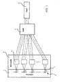
- a lens array 4 of a micro-optics whose individual elements 4 are each aligned with one of the LEDs 3.
- the optical elements of the lens array 4 in turn are designed and aligned so that the light beams of the individual LED elements 3 are focused on a collection optics 5, which is preferably arranged in front of or on an optical fiber 6 collecting optics 5, for example, a ball lens.
Landscapes
- Physics & Mathematics (AREA)
- General Physics & Mathematics (AREA)
- Optics & Photonics (AREA)
- Optical Couplings Of Light Guides (AREA)
- Testing Or Measuring Of Semiconductors Or The Like (AREA)
- Led Device Packages (AREA)
- Investigating Materials By The Use Of Optical Means Adapted For Particular Applications (AREA)
- Instruments For Measurement Of Length By Optical Means (AREA)
Description
- Die Erfindung betrifft eine Lichtquelle spektraler Breitbandigkeit mit hoher Lichtleistung für faseroptische Anwendungen, insbesondere für den Einsatz in faseroptischen Interferometern oder faseroptischen Gyroskopen (FOGs).
- Bisher werden in faseroptischen Sensoren, insbesondere in FOGs, Superlumineszenz-Dioden als Lichtquelle verwendet, um die beiden zentralen Anforderungen von spektraler Breitbandigkeit einerseits und ausreichender in die Faser einzukoppelnder Lichtleistung andererseits zu garantieren. Solche Lichtquellen sind Spezialbauteile, die aufgrund ihrer geringen Stückzahl vergleichsweise sehr teuer sind. Handelsübliche, billige Alternativen wären lichtemittierende Dioden (LEDs) oder Laserdioden (LDs). LEDs erfüllen das Leistungskriterium nicht, LDs andererseits weisen nicht die zu fordernden spektralen Eigenschaften auf.
- Der Erfindung liegt damit die Aufgabe zugrunde, eine spektral breitbandige Lichtquelle hoher Lichtleistung für faseroptische Anwendungen zur Verfügung zu stellen, die sich in einem wirtschaftlichen automatischen Massenherstellungsprozess und damit in großen Stückzahlen preisgünstig herstellen lässt.
- Eine spektral breitbandige Lichtquelle mit vergleichsweise hoher Lichtleistung für faseroptische Anwendungen, insbesondere für faseroptische Sensoren, ist erfindungsgemäß gekennzeichnet durch ein auf einem Substrat, insbesondere einem Wafer oder Chip angeordnetes monolithisches Linear-Array von benachbarten oberffächenemittierenden LEDs, eine vor dem monolithischen LED-Linear-Array auf der Abstrahlseite in vorgegebenem Abstand angeordnete Mikrooptik mit den LED-Elementen individuell zugeordneten optischen Funktionen derart, dass die Abstrahlung der einzelnen LEDs auf eine zur Optimierung der in eine optische Faser einkoppelbaren Lichtleistung auf eine vor der Einkoppelstelle der Faser angeordnete Optik-Einheit gebündelt wird.
- Vorzugsweise ist die Optik-Einheit als eine an einem Lichteinstrahlende der Faser angeordnete Kugellinse ausgebildet.
- Außer für faseroptische Sensoren eignet sich die Erfindung auch vorteilhaft für bestimmte Anwendungen in der Messtechnik, insbesondere in der Telekommunikation, d. h. überall dort, wo eine spektrale Breitbandigkeit benötigt wird, z. B. bei der Vermessung/Einmessung von WDM- oder DWDM-Systemen.
- Der Erfindungsgedanke besteht also in der geeigneten Kombination von mehreren grundsätzlich zur Verfügung stehenden Techniken und Elementen, nämlich
- leistungsstarken LEDs,
- präzisen Mikrooptiken zur Strahlbündelung der von den einzelnen LEDs abgegebenen Lichter, und
- einer geeigneten weiteren Optik zur optimierten Einkoppelung der gebündelten Lichtleistung in eine optische Faser.
- Die eigentliche Lichtquelle ist ein Array, vorzugsweise ein Linsen-Array in Kombination mit leistungsstarken, oberflächenemittierenden LEDs. Mit diesen lässt sich das Kriterium der spektralen Breitbandigkeit erfüllen. Solche LEDs können auf dem gemeinsamen Wafer komplett getestet werden. Das Array besteht aus in geringem Abstand benachbarten LEDs auf dem Wafer, deren jeweilige Anzahl durch die nachfolgenden optischen Einheiten zur Strahlablenkung und Fokussierung sowie durch die erforderliche Lichtleistung bestimmt wird.
- Auf dem monolithischen LED-Array wird eine spezielle Mikrooptik angebracht. Diese besteht aus einem Array einzelner optischer Funktionen, um die mehr oder weniger räumliche Abstrahlung der einzelnen LEDs auf dem Chip in eine jeweils parallele Abstrahlung zu bündeln. Durch diese Summierung der individuellen Lichtleistungen der einzelnen LEDs wird das Kriterium der erwünschten hohen Lichtleistung erfüllt. Durch die Verwendung neuester Verfahren aus den Bereichen der Mikrooptik erreicht man komplexe optische Funktionalität bei gleichzeitig sehr guter Anpassung an das LED-Array. Die Bündelung erfolgt dabei sehr präzise in Anpassung auf die einzelnen LEDs des Arrays und wird gegebenenfalls für jede dieser LEDs des Arrays hinsichtlich der Abstrahlrichtung optimiert. Diese Anforderungen lassen sich mit einer Mikrooptik sehr gut, nämlich monolithisch in einem einzigen Modul realisieren. Eine weitere Optikeinheit, z. B. eine auf der Faser stirnseitig angebrachte Kugellinse dient zur Strahlbündelung und zur Optimierung der Einkopplung in die Faser.
- Ein Ausführungsbeispiel der Erfindung wird nachfolgend unter Bezug auf die Zeichnung der Fig. 1 (einzige Figur) in Einzelheiten erläutert.
- Auf einem Substrat 1, insbesondere einem geeigneten Wafer oder Chip-Substrat ist entlang einer Bezuglinie oder Kante 7 ein Linear-Array von vorzugsweise gleich beabstandeten leistungsstarken und oberflächenemittierenden LEDs ausgebildet, die alle unmittelbar auf dem Wafer mit bekannten Testverfahren komplett getestet werden können. In Abstrahlrichtung der LEDs 3 befindet sich in einem geringen Abstand ein Linsen-Array 4 einer Mikrooptik, deren einzelne Elemente 4 jeweils auf eine der LEDs 3 ausgerichtet sind. Die Optikelemente des Linsen-Arrays 4 ihrerseits sind so gestaltet und ausgerichtet, dass die Lichtstrahlen der einzelnen LED-Elemente 3 auf eine Sammeloptik 5 fokussiert werden, die vorzugsweise eine vor oder auf einer optischen Faser 6 angeordnete Sammeloptik 5, beispielsweise eine Kugellinse ist.
- Mit der Erfindung werden folgende wesentliche Vorteile erreicht:
- 1. Wesentliche Bearbeitungs- und Testschritte können als Batch-Processing durchgeführt werden. Dies führt zu deutlich geringeren Herstellungskosten, insbesondere bei der Chip-Herstellung und im Vergleich zu den Herstellungskosten für eine einzelne Superlumineszenzdiode mit vergleichbaren Eigenschaften.
- 2. Die Herstellung des Chips mit dem LED-Linear-Array und dem Linsen-Array erfolgt mit bekannten Prozessen einer Massenfertigung.
- 3. Die Chips können vergleichsweise einfach an den jeweils aktuellen Stand der Technik angepasst werden, um ein Wachstumspotential dieser neuen Technik einfach zu nutzen, die im Prinzip von einer Mehrzahl von Chip-Herstellern heute beherrscht wird.
Claims (2)
- Spektral breitbandige Lichtquelle hoher Lichtleistung für faseroptische Anwendungen, mit- einem auf einem Substrat, insbesondere einem Wafer oder Chip angeordneten Linear-Array von benachbarten oberflächenemittierenden LEDs (3);- einem vor dem LED-Linear-Array auf der Abstrahlseite in vorgegebenem Abstand angeordneten Mikrooptik-Array (4) mit den LED-Elementen individuell zugeordneten optischen Funktionen derart, dass die Abstrahlung der einzelnen LEDs auf eine zur Optimierung der in eine optische Faser (6) einkoppelbaren Lichtleistung dienenden Optik-Einheit (5) gebündelt wird, die vor der Einkoppelstelle der Faser angeordnet ist,dadurch gekennzeichnet,
dass das Linear-Array eine monolithische Einheit bildet und die einzelnen Elemente des Mikrooptik-Arrays (4) so angeordnet bzw. ausgestaltet sind, dass die durch die Elemente abgestrahlten, auf die Optik-Einheit zulaufenden Lichtstrahlen hinsichtlich der Längsachse der Faser unterschiedliche Neigungswinkel aufweisen. - Spektral breitbandige Lichtquelle nach Anspruch 1, dadurch gekenzeichnet, dass die Optik-Einheit (5) als eine an einem Lichteinstrahlende der Faser (6) angeordnete Sammeloptik, insbesondere als Kugellinse ausgebildet ist.
Applications Claiming Priority (3)
| Application Number | Priority Date | Filing Date | Title |
|---|---|---|---|
| DE10245526A DE10245526B4 (de) | 2002-09-30 | 2002-09-30 | Spektral breitbandige Lichtquelle hoher Lichtleistung |
| DE10245526 | 2002-09-30 | ||
| PCT/EP2003/008441 WO2004034112A1 (de) | 2002-09-30 | 2003-07-30 | Spektral breitbandige lichtquelle hoher lichtleistung |
Publications (2)
| Publication Number | Publication Date |
|---|---|
| EP1546785A1 EP1546785A1 (de) | 2005-06-29 |
| EP1546785B1 true EP1546785B1 (de) | 2007-01-03 |
Family
ID=32009977
Family Applications (1)
| Application Number | Title | Priority Date | Filing Date |
|---|---|---|---|
| EP03807765A Expired - Lifetime EP1546785B1 (de) | 2002-09-30 | 2003-07-30 | Spektral breitbandige lichtquelle hoher lichtleistung |
Country Status (4)
| Country | Link |
|---|---|
| US (1) | US20060056772A1 (de) |
| EP (1) | EP1546785B1 (de) |
| DE (2) | DE10245526B4 (de) |
| WO (1) | WO2004034112A1 (de) |
Families Citing this family (7)
| Publication number | Priority date | Publication date | Assignee | Title |
|---|---|---|---|---|
| DE10250912B4 (de) | 2002-10-31 | 2006-04-27 | Osram Opto Semiconductors Gmbh | Einkoppelvorrichtung |
| WO2006032160A1 (de) | 2004-09-21 | 2006-03-30 | Volpi Ag | Beleuchtungsquelle |
| DE102005022175A1 (de) * | 2005-05-13 | 2006-12-21 | Carl Zeiss Jena Gmbh | Multispektrale Beleuchtungseinheit |
| DE102007027615B4 (de) * | 2007-06-12 | 2012-02-16 | Schott Ag | Vorrichtung zur Einkopplung von Licht in einen faseroptischen Lichtleiter |
| US9941965B2 (en) * | 2015-07-15 | 2018-04-10 | Flextronics Ap, Llc | Laser and optical charging and communications device and method of use |
| CN106526761A (zh) * | 2015-08-26 | 2017-03-22 | 弗莱克斯电子有限责任公司 | Led和激光光束耦合装置及其使用方法 |
| US9970746B2 (en) | 2015-08-26 | 2018-05-15 | Flextronics Ap, Llc | Diffusive optical fiber sensor and communication device and method of use |
Family Cites Families (13)
| Publication number | Priority date | Publication date | Assignee | Title |
|---|---|---|---|---|
| US90172A (en) * | 1869-05-18 | Improvement in horse-stall floors | ||
| US12047A (en) * | 1854-12-05 | Ester | ||
| US4185891A (en) * | 1977-11-30 | 1980-01-29 | Grumman Aerospace Corporation | Laser diode collimation optics |
| US4826269A (en) * | 1987-10-16 | 1989-05-02 | Spectra Diode Laboratories, Inc. | Diode laser arrangement forming bright image |
| JPH04255280A (ja) * | 1991-02-07 | 1992-09-10 | Nippon Steel Corp | 半導体レーザ励起固体レーザ装置 |
| US5268978A (en) * | 1992-12-18 | 1993-12-07 | Polaroid Corporation | Optical fiber laser and geometric coupler |
| US5513201A (en) * | 1993-04-30 | 1996-04-30 | Nippon Steel Corporation | Optical path rotating device used with linear array laser diode and laser apparatus applied therewith |
| WO1996004584A1 (en) * | 1994-07-29 | 1996-02-15 | Polaroid Corporation | Device for optically converting a plurality of beams |
| JP3228098B2 (ja) * | 1995-11-01 | 2001-11-12 | 横河電機株式会社 | 光 源 |
| US5617492A (en) * | 1996-02-06 | 1997-04-01 | The Regents Of The University Of California | Fiber optic coupling of a microlens conditioned, stacked semiconductor laser diode array |
| US6577332B2 (en) * | 1997-09-12 | 2003-06-10 | Ricoh Company, Ltd. | Optical apparatus and method of manufacturing optical apparatus |
| US6654151B1 (en) * | 1999-06-25 | 2003-11-25 | Matsushita Electric Industrial Co., Ltd. | Image projector |
| JP2002202442A (ja) * | 2000-11-06 | 2002-07-19 | Fuji Photo Film Co Ltd | 合波レーザー光源および露光装置 |
-
2002
- 2002-09-30 DE DE10245526A patent/DE10245526B4/de not_active Expired - Fee Related
-
2003
- 2003-07-30 EP EP03807765A patent/EP1546785B1/de not_active Expired - Lifetime
- 2003-07-30 US US10/529,571 patent/US20060056772A1/en not_active Abandoned
- 2003-07-30 DE DE50306218T patent/DE50306218D1/de not_active Expired - Fee Related
- 2003-07-30 WO PCT/EP2003/008441 patent/WO2004034112A1/de not_active Ceased
Also Published As
| Publication number | Publication date |
|---|---|
| WO2004034112A1 (de) | 2004-04-22 |
| EP1546785A1 (de) | 2005-06-29 |
| DE10245526B4 (de) | 2005-05-12 |
| DE10245526A1 (de) | 2004-04-15 |
| US20060056772A1 (en) | 2006-03-16 |
| DE50306218D1 (de) | 2007-02-15 |
Similar Documents
| Publication | Publication Date | Title |
|---|---|---|
| EP0873534B1 (de) | Optoelektronische sendebaugruppe | |
| EP2881031B1 (de) | Endoskop, Exoskop oder Mikroskop und Verfahren zur Beleuchtung eines Betätigungsbereiches eines Endoskops, Exoskops oder Mikroskops | |
| US6384612B2 (en) | Method and apparatus for testing the light output of light emitting devices | |
| DE60214186T2 (de) | Verfahren zur Herstellung von optischen Faserkollimatoren im Array | |
| EP1081819A3 (de) | Optische Anordnung zur Verwendung bei einer Laserdiodenanordnung sowie Laserdiodenanordnung mit einer solchen optischen Anordnung | |
| DE102005031132B4 (de) | Optoelektronisches Modul mit hohem Kopplungswirkungsgrad | |
| AT500056B1 (de) | Optikelement für verkehrszeichen, anzeigetafeln oder dgl. | |
| TW200746274A (en) | Laser irradiation device, laser irradiation method, and method for manufacturing modified object | |
| DE102011107895A1 (de) | Optoelektronisches Modul mit Linsensystem | |
| WO2013010634A1 (de) | Optoelektronisches modul mit verbesserter optik | |
| EP0660467A1 (de) | Optoelektronisches Bauelement und Verfahren zu dessen Herstellung | |
| DE102017109083A1 (de) | Beleuchtungsvorrichtung und Verfahren zur Herstellung einer Beleuchtungsvorrichtung | |
| EP1546785B1 (de) | Spektral breitbandige lichtquelle hoher lichtleistung | |
| DE19830360A1 (de) | Opto-elektronischer Modul | |
| KR20060049790A (ko) | 표면 조명 장치 | |
| WO2006080534B1 (en) | Illumination optical apparatus and optical apparatus | |
| WO2018109226A2 (de) | Segmentierte optik für ein beleuchtungsmodul zur winkelaufgelösten beleuchtung | |
| EP0115267B1 (de) | Abbildungssystem | |
| DE10356384A1 (de) | Werkzeugbeleuchtungsvorrichtung | |
| DE19605726A1 (de) | Anordnung zur optischen Ankopplung einer Monitordiode an eine Laserdiode | |
| EP2159599A3 (de) | Optoelektronischer sensor | |
| US10400971B2 (en) | Lighting module with dioptric interface for motor vehicle | |
| EP0903823A3 (de) | Laserbauelement mit einem Laserarray und Verfahren zu dessen Herstellung | |
| CN103363442A (zh) | 透镜单元、光照射单元以及光照射装置 | |
| DE60101452T2 (de) | Einstückiges optisches element zur lichttransmission und mehrkanaliger optischer modul mit diesen elementen |
Legal Events
| Date | Code | Title | Description |
|---|---|---|---|
| PUAI | Public reference made under article 153(3) epc to a published international application that has entered the european phase |
Free format text: ORIGINAL CODE: 0009012 |
|
| 17P | Request for examination filed |
Effective date: 20050126 |
|
| AK | Designated contracting states |
Kind code of ref document: A1 Designated state(s): AT BE BG CH CY CZ DE DK EE ES FI FR GB GR HU IE IT LI LU MC NL PT RO SE SI SK TR |
|
| RBV | Designated contracting states (corrected) |
Designated state(s): CZ DE FR GB |
|
| GRAP | Despatch of communication of intention to grant a patent |
Free format text: ORIGINAL CODE: EPIDOSNIGR1 |
|
| GRAS | Grant fee paid |
Free format text: ORIGINAL CODE: EPIDOSNIGR3 |
|
| GRAA | (expected) grant |
Free format text: ORIGINAL CODE: 0009210 |
|
| AK | Designated contracting states |
Kind code of ref document: B1 Designated state(s): CZ DE FR GB |
|
| REG | Reference to a national code |
Ref country code: GB Ref legal event code: FG4D Free format text: NOT ENGLISH |
|
| GBT | Gb: translation of ep patent filed (gb section 77(6)(a)/1977) |
Effective date: 20070124 |
|
| REF | Corresponds to: |
Ref document number: 50306218 Country of ref document: DE Date of ref document: 20070215 Kind code of ref document: P |
|
| ET | Fr: translation filed | ||
| PLBE | No opposition filed within time limit |
Free format text: ORIGINAL CODE: 0009261 |
|
| STAA | Information on the status of an ep patent application or granted ep patent |
Free format text: STATUS: NO OPPOSITION FILED WITHIN TIME LIMIT |
|
| 26N | No opposition filed |
Effective date: 20071005 |
|
| GBPC | Gb: european patent ceased through non-payment of renewal fee |
Effective date: 20070730 |
|
| PG25 | Lapsed in a contracting state [announced via postgrant information from national office to epo] |
Ref country code: DE Free format text: LAPSE BECAUSE OF NON-PAYMENT OF DUE FEES Effective date: 20080201 |
|
| PG25 | Lapsed in a contracting state [announced via postgrant information from national office to epo] |
Ref country code: CZ Free format text: LAPSE BECAUSE OF NON-PAYMENT OF DUE FEES Effective date: 20070730 Ref country code: GB Free format text: LAPSE BECAUSE OF NON-PAYMENT OF DUE FEES Effective date: 20070730 |
|
| REG | Reference to a national code |
Ref country code: FR Ref legal event code: ST Effective date: 20080331 |
|
| PG25 | Lapsed in a contracting state [announced via postgrant information from national office to epo] |
Ref country code: FR Free format text: LAPSE BECAUSE OF NON-PAYMENT OF DUE FEES Effective date: 20070731 |