EP1545018B1 - Demodulationsverfahren von mit einem On-Off-Keying Modulationsverfahren kodierter Ultrabreitbandpulssequenzen - Google Patents
Demodulationsverfahren von mit einem On-Off-Keying Modulationsverfahren kodierter Ultrabreitbandpulssequenzen Download PDFInfo
- Publication number
- EP1545018B1 EP1545018B1 EP03293200A EP03293200A EP1545018B1 EP 1545018 B1 EP1545018 B1 EP 1545018B1 EP 03293200 A EP03293200 A EP 03293200A EP 03293200 A EP03293200 A EP 03293200A EP 1545018 B1 EP1545018 B1 EP 1545018B1
- Authority
- EP
- European Patent Office
- Prior art keywords
- pulse sequence
- symbol
- pulse
- signal
- threshold value
- Prior art date
- Legal status (The legal status is an assumption and is not a legal conclusion. Google has not performed a legal analysis and makes no representation as to the accuracy of the status listed.)
- Expired - Lifetime
Links
Images
Classifications
-
- H—ELECTRICITY
- H04—ELECTRIC COMMUNICATION TECHNIQUE
- H04L—TRANSMISSION OF DIGITAL INFORMATION, e.g. TELEGRAPHIC COMMUNICATION
- H04L27/00—Modulated-carrier systems
- H04L27/02—Amplitude-modulated carrier systems, e.g. using on-off keying; Single sideband or vestigial sideband modulation
- H04L27/06—Demodulator circuits; Receiver circuits
-
- H—ELECTRICITY
- H04—ELECTRIC COMMUNICATION TECHNIQUE
- H04B—TRANSMISSION
- H04B1/00—Details of transmission systems, not covered by a single one of groups H04B3/00 - H04B13/00; Details of transmission systems not characterised by the medium used for transmission
- H04B1/69—Spread spectrum techniques
- H04B1/7163—Spread spectrum techniques using impulse radio
- H04B1/71637—Receiver aspects
Definitions
- the present invention relates to a method for transmitting data in a telecommunication system including at least one transmitter and one receiver, said transmitter being intended to transmit a signal formed by at least one sequence of Ns pulses over Ns time windows, each pulse being enclosed within a time chip whose position whithin its relevant time window is defined by a chip number.
- each transmitter may be identified by a signature formed by the above-mentioned chip numbers, which signature is in itself quite sturdy and may thus be reliably and accurately communicated to all potential receivers.
- the pulses used in UWB systems are very short, having for example a duration lower than 0,1 nanosecond, which offers to such systems bandwidths at least as large as 10 GigaHertz, entailing high flexibility and hence numerous possible applications for such systems.
- the above-described signal may form a carrying signal on which information can be encoded by modulation of said carrying signal.
- the inventors have observed that, because of the shortness of the pulses involved, a precise synchronization with a given pulse sequence will be difficult to perform at the receiver end, so that the chosen modulation scheme should involve as few time-related parameters as possible in order to be cost-efficient.
- the present invention thus aims at providing a modulation/demodulation scheme according to which the information carried by pulse sequences may be recovered at the receiver end without said receiver having to map precisely, with respect to time, the received pulse sequences.
- a method for transmitting data as described in the opening paragraph is characterized according to the invention in that it includes at least one symbol decoding step to be executed at the receiver end, in the course of which symbol decoding step at least one modulation value representative of an amount of power carried by each pulse sequence is computed and compared to at least one predetermined threshold value, which threshold value will have been computed beforehand by equating a first and a second probability density function representing a likelihood for the transmitted signal to carry a first symbol and a likelihood for the transmitted signal to carry a second symbol, respectively.
- the symbol decoding step according to the invention enables to achieve a demodulation of a modulated UWB symbol in a very straightforward manner, by quantifying the power of the received signal and performing simple comparisons with one or several threshold values, which comparisons are easy to implement.
- Such a demodulation scheme does not require the receiver to perform a precise mapping, with respect to time, of the received signal, which in turn enables to manufacture adapted receivers at a relatively low cost.
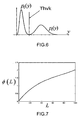
- each predermined threshold value may be predefined and for example set at 1/2 or 3/4 if Vki is to be chosen among integer values 0 and 1.
- the inventors have observed, however, that such fixed thresholds, which do not take into account communication conditions between the transmitter end the receiver may generate decoding errors.
- the inventors thus have designed a thresholding scheme based on an equation of two probability densities, each taking into account real-time communication conditions, so that neither gray zone nor overlap will exist between two interpreting conditions.
- the polynom defining the threshold value will preferably be limited to the second order in order to achieve a suitable balance between computing complexity and decoding efficiency.
- a first-order coefficient of the polynom defining the threshold value is given by an ordinate of a curve whose abcissis is formed by an energy ratio related to the transmission of the relevant pulse sequence.
- the modulation of the UWB signals to be demodulated by carrying out such a symbol decoding step may result from various modulation schemes.
- a method as described hereinbefore further includes at least one symbol encoding step to be executed before transmission of said pulse sequence, in the course of which symbol encoding step each pulse sequence is multiplied by an integer value representative of a symbol to be carried by said pulse sequence.
- the information carried by signals transmitted in Ultra-Wide Band telecommunication systems according to the invention will essentially be related to the power carried by these signals, which power is related to the amplitude of the pulses included within such a signal.
- Such a modulation scheme is easy to implement, which in turn enables to manufacture adapted transmitters at a relatively low cost.
- each signal to be transmitted is constituted by a superimposition of a predetermined number of pulse sequences, each pulse sequence having been subjected to a symbol encoding step and corresponding to one of several sub-bands into which a total bandwidth available for transmission has previously been divided.
- This variant of the invention enables to transmit simultaneously several symbols through a same communication channel, and thus to significantly increase the throughput of a telecommunication system in which such a variant of the invention is embodied.
- the invention also relates to a telecommunication system including at least one transmitter and one receiver, said transmitter being intended to transmit a signal formed by at least one pulse sequence of Ns pulses over Ns time windows, each pulse being enclosed within a time chip whose position whithin its relevant time window is defined by a chip number, system in which the receiver includes symbol decoding means intended to compute at least one modulation value representative of an amount of power carried by each pulse sequence and to compare said modulation value to at least one predetermined threshold value obtained by equating a first and a second probability density function representing the likelihood for the transmitted signal to carry a first symbol and the likelihood for the transmitted signal to carry a second symbol, respectively.
- the transmitter includes symbol encoding means intended to multiply each pulse sequence by one of two integer values representative of a symbol to be carried by said pulse sequence.
- the transmitter further includes signal combination means intended to receive a predetermined number of pulse sequences, each pulse sequence having been generated by symbol encoding means and corresponding to one of several sub-bands into which a total bandwidth available for transmission has previously been divided, said signal combination means being intended to combine all said pulse sequences into a signal to be transmitted.
- the invention also relates to a device intended to receive a signal formed by at least one sequence of Ns pulses over Ns time windows, each pulse being enclosed within a time chip whose position whithin its relevant time window is defined by a chip number, which receiver includes symbol decoding means intended to compute at least one modulation value representative of an amount of power carried by each pulse sequence and to compare said modulation value to at least one predetermined threshold value obtained by equating a first and a second probability density function representing the likelihood for the transmitted signal to carry a first symbol and the likelihood for the transmitted signal to carry a second symbol, respectively.
- the invention also relates to a device intended to transmit a signal formed by at least one sequence of Ns pulses over Ns time windows, each pulse being enclosed within a time chip whose position whithin its relevant time window is defined by a chip number, which transmitter includes symbol encoding means intended to multiply each pulse sequence by one of two integer values representative of a symbol to be carried by said pulse sequence.
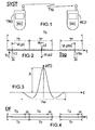
- Fig. 1 depicts a telecommunication system SYST in which the present invention is embodied.
- This system SYST includes at least one transmitter TRD and one receiver RCD, which may for example be both constituted by devices such as mobile phones.
- the number Ns of pulses included in this sequence may, for example, be chosen equal to 128, while the width of each time window may be chosen equal to 100 nanoseconds, with a width of 1 nanosecond for each time chip.
- the transmitter TRD includes symbol encoding means ENC intended to multiply each pulse sequence by an integer value representative of a symbol to be carried by said pulse sequence.
- the information carried by the transmitted signal Tsg will thus essentially be related to the power carried by this signal Tsg, which power is related to the amplitude of the pulses included within said signal Tsg. This information may then be recovered by the receiver RCD without said receiver RCD having to map precisely, with respect to time, the received pulse sequences.
- the receiver RCD includes symbol decoding means DEC intended to compute at least one modulation value representative of an amount of power carried by each pulse sequence and to compare said modulation value to at least one predetermined threshold value.
- symbol decoding means DEC intended to compute at least one modulation value representative of an amount of power carried by each pulse sequence and to compare said modulation value to at least one predetermined threshold value.
- Such frequency interference should be limited as a rule, and is targeted by a European Commission Directive 83/336 CEE, as well as by regulation of the USA's Federal Communications Commission.
- This time-jitter introduced by time-delaying means, will be kept small with respect to a delay spread induced by a communication channel through which the modulated signal will be transmitted.
- the delay spread may have, for example, a value of 100 nanoseconds.
- Such a time-jitter won't affect the information carried by each pulse sequence, and mainly adds an optional degree of flexibility to the modulation scheme according to the invention.
- the information to be carried by the transmitted signal Tsg will be of a binary nature, so that the integer value Vi representative of a bit to be carried by said pulse sequence will either be equal to 1 or to 0.
- Fig.3 is another chronogram which depicts a possible shape p(t) which may be chosen for constituting the above-mentioned pulses.
- p t A . 1 - 4 ⁇ ⁇ ⁇ t / Tw 2 . exp - 2 ⁇ ⁇ ⁇ t / Tw 2 .
- Fig.4 is yet another chronogram which depicts a dataframe DF formed by successive pulse sequences such as the one described above, each having a total duration Ts, a guard interval GI being periodically inserted between two such sequences in order to prevent alteration of a given sequence by a following one, which alterations coud be caused, for example, by intermodulation products between said pulse sequences.
- a device intended to receive such a data frame DF must thus only be able to measure quantities representative of the successive amounts of power carried by the successive pulse sequences in order to identify the informational content of the dataframe DF, without having to map precisely, with respect to time, the received pulse sequences.
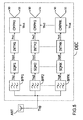
- Fig.5 depicts symbol decoding means DEC included in a receiver according to an embodiment of the invention, in which embodiment the transmitted signal Tsg is a composite signal including a combination of K pulse sequences as described hereinbefore, each pulse sequence having thus been subjected to a symbol encoding step at the transmitting end.
- This receiver includes an antenna device ANT intended to receive such a composite signal Tsg.
- This embodiment enables to transmit simultaneously several symbols through a same communication channel, and thus to significantly increase the throughput of a telecommunication system in which such a variant of the invention is embodied.
- a modulation value Pwk may for example be computed as the integral, on the duration of the channel delay, of the square signal Sqsk delivered by the related squaring module SQMk.
- Each squaring module SQMk may be formed by a Gilbert cell fed with identical input signals.
- Each integrating module INTk may be formed by an operational amplifier provided with an RC feedback.
- Each comparing module CMPMk may be formed by an operational amplifier intended to receive a given modulation value Pwk and the predermined threshold value Thvk assigned to this comparing module CMPMk.
- the symbol decoding means DEC may thus be formed by off-the-shelf analog circuits, which analog circuits are known for their high processing speed and do not require any sampling, as opposed to digital solutions, which will enable to further reduce the processing power and the time required for performing a signal decoding step according to this embodiment of the invention.
- Each predermined threshold value may be predefined and for example set at 1/2 or 3/4 if Vki is to be chosen among integer values 0 and 1.
- the inventors have observed, however, that such fixed thresholds, which do not take into account communication conditions between the transmitter end the receiver may generate decoding errors.
- the inventors thus have designed a thresholding scheme based on an equating of two probability densities, each taking into account real-time communication conditions, so that neither gray zone nor overlap will exist between two interpreting conditions.
- first and second probability densities can be derived from existing art in the field of mathematics applied to optics (A. Bruce Carlson, "Communication Systems An Introduction to Signals and Noise In Electrical Communications, 3 rd Ed.”, McGRAW-HILL, NY).
- E N exp - x + E N
- ⁇ denotes the Euler function and Ij the jth Bessel function of the first kind
- E being an energy carried by the pulse sequence and computed by integrating the transmitted signal over a given time period Ti
- N being a noise intensity adversely affecting the transmission of said signal
- B being a bandwidth of the pulse sequence for which the threshold value is computed.
- the threshold value is defined by a polynom of a variable M 1 ⁇ 2 , which is an approximation of the solution of the above equation system and enables to avoid the computation of an optimal solution to said system.
Landscapes
- Engineering & Computer Science (AREA)
- Computer Networks & Wireless Communication (AREA)
- Signal Processing (AREA)
- Dc Digital Transmission (AREA)
- Digital Transmission Methods That Use Modulated Carrier Waves (AREA)
Claims (10)
- Verfahren zum Senden von Daten in einem UWB-Telekommunikationssystem mit wenigstens einem Sender (TRD) und einem Empfänger (RCD), wobei der Sender eine Signal (Tsg) sendet, das durch wenigstens eine Pulssequenz von Ns Pulsen über Ns sich nicht überlagernden Fenstern ausgebildet ist, wobei jeder Puls (pj) innerhalb eines Zeitchips eingeschlossen ist, dessen Position innerhalb seines relevanten nicht überlagernden Fensters durch eine Chipnummer (cj) definiert ist, wobei das Verfahren wenigstens einen am Empfängerende auszuführenden Symboldecodierschritt enthält, dadurch gekennzeichnet, dass im Verlauf des Symboldecodierschritts wenigstens ein Modulationswert (Pwk), der eine durch eine jeweilige Pulssequenz getragene Menge an Leistung darstellt, berechnet und mit wenigstens einem Schwellenwert (Thvk) verglichen wird, um ein durch die Pulssequenz getragenes Symbol wiederzugewinnen, ohne eine genaue Abbildung der Pulssequenz in Bezug auf die Zeit zu erfordern, welcher Schwellenwert im Voraus durch Gleichsetzen einer ersten (P0) und einer zweiten (P1) Wahrscheinlichkeitsdichtefunktion berechnet worden sein wird, die jeweils eine Wahrscheinlichkeit dafür, dass das gesendete Signal ein erstes Symbol trägt, und eine Wahrscheinlichkeit dafür, dass das gesendete Signal ein zweites Symbol trägt, darstellt.
- Verfahren nach Anspruch 1, dadurch gekennzeichnet, dass der Schwellenwert (Thvk) durch ein Polynom einer Variablen M1/2 definiert ist, wobei M durch M=(2.B.Ns.Ti+1)/2 definiert ist, wobei B eine Bandbreite der Pulssequenz ist, für die der Schwellenwert berechnet wird, und Ti eine Zeitdauer, über welche eine Integration jedes zur Pulssequenz gehörenden Pulses durchgeführt wird, um die durch die Pulssequenz getragene Menge an Leistung zu berechnen.
- Verfahren nach Anspruch 2, dadurch gekennzeichnet, dass das den Schwellenwert definierende Polynom auf die zweite Ordnung beschränkt ist.
- Verfahren nach einem der Ansprüche 2 oder 3, dadurch gekennzeichnet, dass ein Koeffizient erster Ordnung des den Schwellenwert definierenden Polynoms durch eine Ordinate einer Kurve gegeben ist, deren Abszisse durch eine Energieverhältnis in Bezug auf das Senden der relevanten Pulssequenz gebildet ist.
- Verfahren nach einem der Ansprüche 1 bis 4, wobei das Verfahren weiterhin wenigstens einen vor einem Senden der Pulssequenz auszuführenden Symbolcodierschritt enthält, dadurch gekennzeichnet, dass im Verlauf des Symbolcodierschritts jede Pulssequenz mit einem von zwei ganzzahligen Werten multipliziert wird, die ein durch die Pulssequenz zu tragendes Symbol darstellen.
- Verfahren nach einem der Ansprüche 1 bis 5, dadurch gekennzeichnet, dass jedes zu sendende Signal durch eine Überlagerung einer vorbestimmten Anzahl von Pulssequenzen gebildet wird, wobei jede Pulssequenz einem Symbolcodierschritt unterzogen worden ist und einem von mehreren Unterbändern entspricht, in welche eine gesamte Bandbreite, die für ein Senden verfügbar ist, zuvor aufgeteilt worden ist.
- Empfänger (RCD), der zum Empfangen eines durch einen Sender (TRD) gesendeten Signals (Tsg) geeignet ist, wobei das Signal durch wenigstens eine Sequenz von Ns Pulsen über Ns sich nicht überlagernden Fenstern ausgebildet ist, wobei jeder Puls (pj) innerhalb eines Zeitchips eingeschlossen ist, dessen Position innerhalb seines relevanten Zeitfensters durch eine Chipnummer (cj) definiert ist, dadurch gekennzeichnet, dass der Empfänger (RCD) eine Symboldecodiereinrichtung (DEC) enthält, die wenigstens einen Modulationswert (Pwk), der eine durch jede Pulssequenz getragene Menge an Leistung darstellt, berechnet und den Modulationswert mit wenigstens einem vorbestimmten Schwellenwert (Thvk) vergleicht, um ein durch die Pulssequenz getragenes Symbol wiederzugewinnen, ohne eine genaue Abbildung der Pulssequenz in Bezug auf die Zeit zu erfordern, welcher Schwellenwert durch Gleichsetzen einer ersten (P0) und einer zweiten (P1) Wahrscheinlichkeitsdichtefunktion erhalten wird, die jeweils eine Wahrscheinlichkeit dafür, dass das gesendete Signal ein erstes Symbol trägt, und eine Wahrscheinlichkeit dafür, dass das gesendete Signal ein zweites Symbol trägt, darstellt.
- UWB-Telekommunikationssystem mit wenigsten einem Sender (TRD) und einem Empfänger (RCD) nach Anspruch 7, wobei der Sender dazu geeignet ist, ein Signal (Tsg) zu senden, das durch wenigstens eine Sequenz von Ns Pulsen über Ns sich nicht überlagernden Fenstern ausgebildet ist, wobei jeder Puls (pj) innerhalb eines Zeitchips eingeschlossen ist, dessen Position innerhalb seines relevanten Zeitfensters durch eine Chipnummer (cj) definiert ist
- UWB-Telekommunikationssystem nach Anspruch 8, dadurch gekennzeichnet, dass der Sender eine Symbolcodiereinrichtung (ENC) enthält, die jede Pulssequenz mit einem von zwei ganzzahligen Werten multiplizieren soll, die ein durch die Pulssequenz zu tragendes Symbol darstellen.
- UWB-Telekommunikationssystem nach einem der Ansprüche 8 oder 9, dadurch gekennzeichnet, dass der Sender weiterhin eine Signalkombinationseinrichtung enthält, die eine vorbestimmte Anzahl von Pulssequenzen empfangen soll, wobei jede Pulssequenz durch eine Symbolcodiereinrichtung erzeugt worden ist und einem von mehreren Unterbändern entspricht, in welche eine gesamte Bandbreite, die für ein Senden verfügbar ist, zuvor aufgeteilt worden ist, wobei die Kombinationseinrichtung alle Pulssequenzen in ein zu sendendes Signal kombinieren soll.
Priority Applications (6)
| Application Number | Priority Date | Filing Date | Title |
|---|---|---|---|
| EP03293200A EP1545018B1 (de) | 2003-12-17 | 2003-12-17 | Demodulationsverfahren von mit einem On-Off-Keying Modulationsverfahren kodierter Ultrabreitbandpulssequenzen |
| DE60324440T DE60324440D1 (de) | 2003-12-17 | 2003-12-17 | Demodulationsverfahren von mit einem On-Off-Keying Modulationsverfahren kodierter Ultrabreitbandpulssequenzen |
| AT03293200T ATE413020T1 (de) | 2003-12-17 | 2003-12-17 | Demodulationsverfahren von mit einem on-off- keying modulationsverfahren kodierter ultrabreitbandpulssequenzen |
| US10/998,930 US7817728B2 (en) | 2003-12-17 | 2004-11-30 | Method for demodulating UWB pulse sequences encoded according to an on-off keying modulation scheme |
| CN2004100954035A CN1630211B (zh) | 2003-12-17 | 2004-12-16 | 用于解调根据开关键控调制方案编码的uwb脉冲序列的方法 |
| JP2004366564A JP2005218079A (ja) | 2003-12-17 | 2004-12-17 | 少なくとも1つの送信機および1つの受信機を含む通信システムにおいてデータを送信するための方法、少なくとも1つの送信機および1つの受信機を含む通信システム、ならびにNs個の時間窓にわたってNs個のパルスからなる少なくとも1つの系列によって形成される信号を送信および受信するように構成される装置 |
Applications Claiming Priority (1)
| Application Number | Priority Date | Filing Date | Title |
|---|---|---|---|
| EP03293200A EP1545018B1 (de) | 2003-12-17 | 2003-12-17 | Demodulationsverfahren von mit einem On-Off-Keying Modulationsverfahren kodierter Ultrabreitbandpulssequenzen |
Publications (2)
| Publication Number | Publication Date |
|---|---|
| EP1545018A1 EP1545018A1 (de) | 2005-06-22 |
| EP1545018B1 true EP1545018B1 (de) | 2008-10-29 |
Family
ID=34486485
Family Applications (1)
| Application Number | Title | Priority Date | Filing Date |
|---|---|---|---|
| EP03293200A Expired - Lifetime EP1545018B1 (de) | 2003-12-17 | 2003-12-17 | Demodulationsverfahren von mit einem On-Off-Keying Modulationsverfahren kodierter Ultrabreitbandpulssequenzen |
Country Status (6)
| Country | Link |
|---|---|
| US (1) | US7817728B2 (de) |
| EP (1) | EP1545018B1 (de) |
| JP (1) | JP2005218079A (de) |
| CN (1) | CN1630211B (de) |
| AT (1) | ATE413020T1 (de) |
| DE (1) | DE60324440D1 (de) |
Cited By (1)
| Publication number | Priority date | Publication date | Assignee | Title |
|---|---|---|---|---|
| JP2005218079A (ja) * | 2003-12-17 | 2005-08-11 | Mitsubishi Electric Information Technology Centre Europa Bv | 少なくとも1つの送信機および1つの受信機を含む通信システムにおいてデータを送信するための方法、少なくとも1つの送信機および1つの受信機を含む通信システム、ならびにNs個の時間窓にわたってNs個のパルスからなる少なくとも1つの系列によって形成される信号を送信および受信するように構成される装置 |
Families Citing this family (7)
| Publication number | Priority date | Publication date | Assignee | Title |
|---|---|---|---|---|
| EP1523106B1 (de) * | 2003-10-09 | 2007-08-08 | Mitsubishi Electric Information Technology Centre Europe B.V. | Verfahren zur Demodulation von Ultrabreitbandpulsfolgen |
| ATE400093T1 (de) * | 2003-10-09 | 2008-07-15 | Mitsubishi Electric Corp | Verfahren zur modulation ultrabreitbandiger pulssequenzen |
| KR100690089B1 (ko) | 2005-12-16 | 2007-03-08 | 한국전기연구원 | 비일치성 초광대역 시스템의 비트오율 성능향상을 위한최적임계값 결정방법 |
| CN100362752C (zh) * | 2006-03-21 | 2008-01-16 | 东南大学 | 低复杂度超宽带射频前端的实现方法及装置 |
| CN102761902B (zh) | 2011-04-29 | 2014-07-09 | 华为技术有限公司 | 容量站激活的方法及无线通信装置与系统 |
| CN103503320B (zh) * | 2011-05-23 | 2016-10-05 | 华为技术有限公司 | 用于重构源信号的方法和解码器 |
| CN113644850B (zh) * | 2021-07-12 | 2023-12-22 | 南京国电南自维美德自动化有限公司 | 一种励磁系统的脉冲混合传输方法及系统 |
Family Cites Families (23)
| Publication number | Priority date | Publication date | Assignee | Title |
|---|---|---|---|---|
| US5610907A (en) * | 1994-07-29 | 1997-03-11 | Barrett; Terence W. | Ultrafast time hopping CDMA-RF communications: code-as-carrier, multichannel operation, high data rate operation and data rate on demand |
| US5677927A (en) * | 1994-09-20 | 1997-10-14 | Pulson Communications Corporation | Ultrawide-band communication system and method |
| CN1249098A (zh) * | 1997-03-07 | 2000-03-29 | 贝瑞特控股公司 | 超高速时间跳频cdma-rf的改进 |
| JP2000174830A (ja) * | 1998-12-09 | 2000-06-23 | Nec Corp | Ask復調方法及び装置 |
| US6810087B2 (en) * | 2000-01-04 | 2004-10-26 | General Electric Company | Ultra-wideband communications system |
| US6556621B1 (en) * | 2000-03-29 | 2003-04-29 | Time Domain Corporation | System for fast lock and acquisition of ultra-wideband signals |
| US6937667B1 (en) * | 2000-03-29 | 2005-08-30 | Time Domain Corporation | Apparatus, system and method for flip modulation in an impulse radio communications system |
| US20020075972A1 (en) * | 2000-03-29 | 2002-06-20 | Time Domain Corporation | Apparatus, system and method for one-of-many positions modulation in an impulse radio communications system |
| US7145954B1 (en) * | 2000-06-12 | 2006-12-05 | Time Domain Corporation | Method and apparatus for mapping pulses to a non-fixed layout |
| AU2001270063A1 (en) * | 2000-06-21 | 2002-01-02 | Pulse-Link, Inc. | Ultra wide band base band receiver |
| JP2002325071A (ja) * | 2001-04-25 | 2002-11-08 | Sony Corp | 送信装置、受信装置、送信方法、並びに受信方法 |
| JP2003061057A (ja) * | 2001-08-14 | 2003-02-28 | Sony Corp | 付加データ検出装置及び付加データ検出方法並びに付加データ検出プログラム |
| JP2003152594A (ja) * | 2001-11-19 | 2003-05-23 | Sony Corp | 送信装置およびその方法、受信装置およびその方法、通信システムおよびその方法、ならびにプログラム |
| JP2003174368A (ja) * | 2001-12-06 | 2003-06-20 | Sony Corp | 無線通信装置、送信出力制御方法、記憶媒体、並びにコンピュータ・プログラム |
| JP2003218963A (ja) * | 2001-12-07 | 2003-07-31 | Applied Microcircuits Corp | 非因果的チャネル等化のためのフィードフォワード/フィードバックシステムおよび方法 |
| WO2004032600A2 (en) * | 2002-02-20 | 2004-04-22 | General Atomics | Method and apparatus for data transfer using a time division multiple frequency scheme with additional modulation |
| JP2005518720A (ja) * | 2002-02-20 | 2005-06-23 | エクストリームスペクトラム,インコーポレイテッド | M元直交コード化通信方法及びシステム |
| JP2004208110A (ja) * | 2002-12-26 | 2004-07-22 | Casio Comput Co Ltd | 無線通信システム、受信装置および情報受信方法 |
| WO2004073195A1 (en) * | 2003-02-14 | 2004-08-26 | Koninklijke Philips Electronics N.V. | Variable sign/phase and inter-pulse time modulated multi-band uwb communication system |
| US20040179631A1 (en) * | 2003-03-13 | 2004-09-16 | Telecommunications Research Laboratories | UWB receiver architecture |
| EP1526648A1 (de) * | 2003-10-21 | 2005-04-27 | Mitsubishi Electric Information Technology Centre Europe B.V. | Systeme und Vorrichtung zur Modulation von UWB-Pulssequenzen |
| US7295638B2 (en) * | 2003-11-17 | 2007-11-13 | Motorola, Inc. | Communication device |
| EP1545018B1 (de) * | 2003-12-17 | 2008-10-29 | Mitsubishi Electric Information Technology Centre Europe B.V. | Demodulationsverfahren von mit einem On-Off-Keying Modulationsverfahren kodierter Ultrabreitbandpulssequenzen |
-
2003
- 2003-12-17 EP EP03293200A patent/EP1545018B1/de not_active Expired - Lifetime
- 2003-12-17 DE DE60324440T patent/DE60324440D1/de not_active Expired - Lifetime
- 2003-12-17 AT AT03293200T patent/ATE413020T1/de not_active IP Right Cessation
-
2004
- 2004-11-30 US US10/998,930 patent/US7817728B2/en not_active Expired - Fee Related
- 2004-12-16 CN CN2004100954035A patent/CN1630211B/zh not_active Expired - Fee Related
- 2004-12-17 JP JP2004366564A patent/JP2005218079A/ja active Pending
Cited By (1)
| Publication number | Priority date | Publication date | Assignee | Title |
|---|---|---|---|---|
| JP2005218079A (ja) * | 2003-12-17 | 2005-08-11 | Mitsubishi Electric Information Technology Centre Europa Bv | 少なくとも1つの送信機および1つの受信機を含む通信システムにおいてデータを送信するための方法、少なくとも1つの送信機および1つの受信機を含む通信システム、ならびにNs個の時間窓にわたってNs個のパルスからなる少なくとも1つの系列によって形成される信号を送信および受信するように構成される装置 |
Also Published As
| Publication number | Publication date |
|---|---|
| DE60324440D1 (de) | 2008-12-11 |
| US7817728B2 (en) | 2010-10-19 |
| CN1630211B (zh) | 2010-05-26 |
| ATE413020T1 (de) | 2008-11-15 |
| US20050213673A1 (en) | 2005-09-29 |
| CN1630211A (zh) | 2005-06-22 |
| JP2005218079A (ja) | 2005-08-11 |
| EP1545018A1 (de) | 2005-06-22 |
Similar Documents
| Publication | Publication Date | Title |
|---|---|---|
| Ramirez-Mireles et al. | Multiple-access performance limits with time hopping and pulse position modulation | |
| US20040242155A1 (en) | UWB communication receiver feedback loop | |
| EP1545018B1 (de) | Demodulationsverfahren von mit einem On-Off-Keying Modulationsverfahren kodierter Ultrabreitbandpulssequenzen | |
| EP1568148B1 (de) | Selektive dateninversion in der ultrabreitbandkommunikation zur beseitigung von linienfrequenzen | |
| US20090296831A1 (en) | Wireless Communication Method and System | |
| EP1523106B1 (de) | Verfahren zur Demodulation von Ultrabreitbandpulsfolgen | |
| US7539234B2 (en) | System and device for modulating UWB pulse sequences | |
| EP1635477B1 (de) | Verfahren zur Schätzung von Kommunikationsbedingungen einer drahtlosen Ultrabreitbandverbindung | |
| US7075382B2 (en) | Method and apparatus for modulating a pulse signal with a bit stream | |
| Gomes et al. | Performance evaluation of UWB wireless link | |
| JP2006525760A (ja) | マルチバンド広帯域通信システムにおける個別電力スペクトル密度成分を減少させる方法及び装置 | |
| EP1701453B1 (de) | Verfahren zur kostengünstigen Detektion von Ultrabreitbandpulsfolgen | |
| EP1701454B1 (de) | Verfahren zur kostengünstigen Übertragung von Ultrabreitbandpulsfolgen | |
| US7792210B2 (en) | Method for modulating UWB pulse sequences | |
| EP1622281B1 (de) | Mehrbandiges Ultrabreitbandnachrichtenübertragungssystem mit mehreren Sende- Empfangsantennen | |
| Dowla et al. | Multiple access in ultra-wideband communications using multiple pulses and the use of least squares filters | |
| Khalesehosseini et al. | Generalized CRLB for DA and NDA synchronization of UWB signals with clock offset | |
| Beaulieu et al. | On the PDF of multiple access interference in time-hopping UWB systems |
Legal Events
| Date | Code | Title | Description |
|---|---|---|---|
| PUAI | Public reference made under article 153(3) epc to a published international application that has entered the european phase |
Free format text: ORIGINAL CODE: 0009012 |
|
| AK | Designated contracting states |
Kind code of ref document: A1 Designated state(s): AT BE BG CH CY CZ DE DK EE ES FI FR GB GR HU IE IT LI LU MC NL PT RO SE SI SK TR |
|
| AX | Request for extension of the european patent |
Extension state: AL LT LV MK |
|
| 17P | Request for examination filed |
Effective date: 20050823 |
|
| AKX | Designation fees paid |
Designated state(s): AT BE BG CH CY CZ DE DK EE ES FI FR GB GR HU IE IT LI LU MC NL PT RO SE SI SK TR |
|
| RAP1 | Party data changed (applicant data changed or rights of an application transferred) |
Owner name: MITSUBISHI DENKI KABUSHIKI KAISHA Owner name: MITSUBISHI ELECTRIC INFORMATION TECHNOLOGY CENTRE |
|
| 17Q | First examination report despatched |
Effective date: 20050930 |
|
| GRAP | Despatch of communication of intention to grant a patent |
Free format text: ORIGINAL CODE: EPIDOSNIGR1 |
|
| RIN1 | Information on inventor provided before grant (corrected) |
Inventor name: PAQUELET, STEPHANE,MITSUBISHI ELECTRICITE Inventor name: AUBERT, LOUIS-MARIE,MITSUBISHI ELECTRICITE Inventor name: MEUNIER, CLAIRE,U |
|
| GRAS | Grant fee paid |
Free format text: ORIGINAL CODE: EPIDOSNIGR3 |
|
| GRAA | (expected) grant |
Free format text: ORIGINAL CODE: 0009210 |
|
| AK | Designated contracting states |
Kind code of ref document: B1 Designated state(s): AT BE BG CH CY CZ DE DK EE ES FI FR GB GR HU IE IT LI LU MC NL PT RO SE SI SK TR |
|
| REG | Reference to a national code |
Ref country code: GB Ref legal event code: FG4D |
|
| REG | Reference to a national code |
Ref country code: CH Ref legal event code: EP |
|
| REG | Reference to a national code |
Ref country code: IE Ref legal event code: FG4D |
|
| REF | Corresponds to: |
Ref document number: 60324440 Country of ref document: DE Date of ref document: 20081211 Kind code of ref document: P |
|
| NLV1 | Nl: lapsed or annulled due to failure to fulfill the requirements of art. 29p and 29m of the patents act | ||
| PG25 | Lapsed in a contracting state [announced via postgrant information from national office to epo] |
Ref country code: AT Free format text: LAPSE BECAUSE OF FAILURE TO SUBMIT A TRANSLATION OF THE DESCRIPTION OR TO PAY THE FEE WITHIN THE PRESCRIBED TIME-LIMIT Effective date: 20081029 Ref country code: ES Free format text: LAPSE BECAUSE OF FAILURE TO SUBMIT A TRANSLATION OF THE DESCRIPTION OR TO PAY THE FEE WITHIN THE PRESCRIBED TIME-LIMIT Effective date: 20090209 Ref country code: BG Free format text: LAPSE BECAUSE OF FAILURE TO SUBMIT A TRANSLATION OF THE DESCRIPTION OR TO PAY THE FEE WITHIN THE PRESCRIBED TIME-LIMIT Effective date: 20090129 |
|
| PG25 | Lapsed in a contracting state [announced via postgrant information from national office to epo] |
Ref country code: FI Free format text: LAPSE BECAUSE OF FAILURE TO SUBMIT A TRANSLATION OF THE DESCRIPTION OR TO PAY THE FEE WITHIN THE PRESCRIBED TIME-LIMIT Effective date: 20081029 Ref country code: PT Free format text: LAPSE BECAUSE OF FAILURE TO SUBMIT A TRANSLATION OF THE DESCRIPTION OR TO PAY THE FEE WITHIN THE PRESCRIBED TIME-LIMIT Effective date: 20090330 Ref country code: SI Free format text: LAPSE BECAUSE OF FAILURE TO SUBMIT A TRANSLATION OF THE DESCRIPTION OR TO PAY THE FEE WITHIN THE PRESCRIBED TIME-LIMIT Effective date: 20081029 Ref country code: NL Free format text: LAPSE BECAUSE OF FAILURE TO SUBMIT A TRANSLATION OF THE DESCRIPTION OR TO PAY THE FEE WITHIN THE PRESCRIBED TIME-LIMIT Effective date: 20081029 |
|
| PG25 | Lapsed in a contracting state [announced via postgrant information from national office to epo] |
Ref country code: DK Free format text: LAPSE BECAUSE OF FAILURE TO SUBMIT A TRANSLATION OF THE DESCRIPTION OR TO PAY THE FEE WITHIN THE PRESCRIBED TIME-LIMIT Effective date: 20081029 Ref country code: BE Free format text: LAPSE BECAUSE OF FAILURE TO SUBMIT A TRANSLATION OF THE DESCRIPTION OR TO PAY THE FEE WITHIN THE PRESCRIBED TIME-LIMIT Effective date: 20081029 Ref country code: RO Free format text: LAPSE BECAUSE OF FAILURE TO SUBMIT A TRANSLATION OF THE DESCRIPTION OR TO PAY THE FEE WITHIN THE PRESCRIBED TIME-LIMIT Effective date: 20081029 Ref country code: EE Free format text: LAPSE BECAUSE OF FAILURE TO SUBMIT A TRANSLATION OF THE DESCRIPTION OR TO PAY THE FEE WITHIN THE PRESCRIBED TIME-LIMIT Effective date: 20081029 Ref country code: MC Free format text: LAPSE BECAUSE OF NON-PAYMENT OF DUE FEES Effective date: 20081231 |
|
| REG | Reference to a national code |
Ref country code: CH Ref legal event code: PL |
|
| PG25 | Lapsed in a contracting state [announced via postgrant information from national office to epo] |
Ref country code: IT Free format text: LAPSE BECAUSE OF FAILURE TO SUBMIT A TRANSLATION OF THE DESCRIPTION OR TO PAY THE FEE WITHIN THE PRESCRIBED TIME-LIMIT Effective date: 20081029 Ref country code: CZ Free format text: LAPSE BECAUSE OF FAILURE TO SUBMIT A TRANSLATION OF THE DESCRIPTION OR TO PAY THE FEE WITHIN THE PRESCRIBED TIME-LIMIT Effective date: 20081029 Ref country code: SE Free format text: LAPSE BECAUSE OF FAILURE TO SUBMIT A TRANSLATION OF THE DESCRIPTION OR TO PAY THE FEE WITHIN THE PRESCRIBED TIME-LIMIT Effective date: 20090129 |
|
| PLBE | No opposition filed within time limit |
Free format text: ORIGINAL CODE: 0009261 |
|
| STAA | Information on the status of an ep patent application or granted ep patent |
Free format text: STATUS: NO OPPOSITION FILED WITHIN TIME LIMIT |
|
| PG25 | Lapsed in a contracting state [announced via postgrant information from national office to epo] |
Ref country code: SK Free format text: LAPSE BECAUSE OF FAILURE TO SUBMIT A TRANSLATION OF THE DESCRIPTION OR TO PAY THE FEE WITHIN THE PRESCRIBED TIME-LIMIT Effective date: 20081029 |
|
| 26N | No opposition filed |
Effective date: 20090730 |
|
| PG25 | Lapsed in a contracting state [announced via postgrant information from national office to epo] |
Ref country code: CH Free format text: LAPSE BECAUSE OF NON-PAYMENT OF DUE FEES Effective date: 20081231 Ref country code: IE Free format text: LAPSE BECAUSE OF NON-PAYMENT OF DUE FEES Effective date: 20081217 Ref country code: LI Free format text: LAPSE BECAUSE OF NON-PAYMENT OF DUE FEES Effective date: 20081231 |
|
| PG25 | Lapsed in a contracting state [announced via postgrant information from national office to epo] |
Ref country code: CY Free format text: LAPSE BECAUSE OF FAILURE TO SUBMIT A TRANSLATION OF THE DESCRIPTION OR TO PAY THE FEE WITHIN THE PRESCRIBED TIME-LIMIT Effective date: 20081029 Ref country code: LU Free format text: LAPSE BECAUSE OF NON-PAYMENT OF DUE FEES Effective date: 20081217 Ref country code: HU Free format text: LAPSE BECAUSE OF FAILURE TO SUBMIT A TRANSLATION OF THE DESCRIPTION OR TO PAY THE FEE WITHIN THE PRESCRIBED TIME-LIMIT Effective date: 20090430 |
|
| PG25 | Lapsed in a contracting state [announced via postgrant information from national office to epo] |
Ref country code: TR Free format text: LAPSE BECAUSE OF FAILURE TO SUBMIT A TRANSLATION OF THE DESCRIPTION OR TO PAY THE FEE WITHIN THE PRESCRIBED TIME-LIMIT Effective date: 20081029 |
|
| PG25 | Lapsed in a contracting state [announced via postgrant information from national office to epo] |
Ref country code: GR Free format text: LAPSE BECAUSE OF FAILURE TO SUBMIT A TRANSLATION OF THE DESCRIPTION OR TO PAY THE FEE WITHIN THE PRESCRIBED TIME-LIMIT Effective date: 20090130 |
|
| PGFP | Annual fee paid to national office [announced via postgrant information from national office to epo] |
Ref country code: GB Payment date: 20101112 Year of fee payment: 8 |
|
| PGFP | Annual fee paid to national office [announced via postgrant information from national office to epo] |
Ref country code: FR Payment date: 20120110 Year of fee payment: 9 |
|
| PGFP | Annual fee paid to national office [announced via postgrant information from national office to epo] |
Ref country code: DE Payment date: 20111216 Year of fee payment: 9 |
|
| GBPC | Gb: european patent ceased through non-payment of renewal fee |
Effective date: 20121217 |
|
| REG | Reference to a national code |
Ref country code: FR Ref legal event code: ST Effective date: 20130830 |
|
| REG | Reference to a national code |
Ref country code: DE Ref legal event code: R119 Ref document number: 60324440 Country of ref document: DE Effective date: 20130702 |
|
| PG25 | Lapsed in a contracting state [announced via postgrant information from national office to epo] |
Ref country code: DE Free format text: LAPSE BECAUSE OF NON-PAYMENT OF DUE FEES Effective date: 20130702 |
|
| PG25 | Lapsed in a contracting state [announced via postgrant information from national office to epo] |
Ref country code: FR Free format text: LAPSE BECAUSE OF NON-PAYMENT OF DUE FEES Effective date: 20130102 Ref country code: GB Free format text: LAPSE BECAUSE OF NON-PAYMENT OF DUE FEES Effective date: 20121217 |