EP1544957A1 - Printed circuit board plug-in connection - Google Patents
Printed circuit board plug-in connection Download PDFInfo
- Publication number
- EP1544957A1 EP1544957A1 EP04028961A EP04028961A EP1544957A1 EP 1544957 A1 EP1544957 A1 EP 1544957A1 EP 04028961 A EP04028961 A EP 04028961A EP 04028961 A EP04028961 A EP 04028961A EP 1544957 A1 EP1544957 A1 EP 1544957A1
- Authority
- EP
- European Patent Office
- Prior art keywords
- connector
- wall
- circuit board
- printed circuit
- contact elements
- Prior art date
- Legal status (The legal status is an assumption and is not a legal conclusion. Google has not performed a legal analysis and makes no representation as to the accuracy of the status listed.)
- Withdrawn
Links
- 238000003780 insertion Methods 0.000 claims description 42
- 230000037431 insertion Effects 0.000 claims description 42
- 230000013011 mating Effects 0.000 claims description 2
- 238000000034 method Methods 0.000 description 13
- 230000008878 coupling Effects 0.000 description 2
- 238000010168 coupling process Methods 0.000 description 2
- 238000005859 coupling reaction Methods 0.000 description 2
- 238000006073 displacement reaction Methods 0.000 description 2
- 238000009434 installation Methods 0.000 description 2
- 230000001154 acute effect Effects 0.000 description 1
- 239000000470 constituent Substances 0.000 description 1
- 230000002349 favourable effect Effects 0.000 description 1
- 238000012986 modification Methods 0.000 description 1
- 230000004048 modification Effects 0.000 description 1
- 230000000284 resting effect Effects 0.000 description 1
Images


Classifications
-
- H—ELECTRICITY
- H01—ELECTRIC ELEMENTS
- H01R—ELECTRICALLY-CONDUCTIVE CONNECTIONS; STRUCTURAL ASSOCIATIONS OF A PLURALITY OF MUTUALLY-INSULATED ELECTRICAL CONNECTING ELEMENTS; COUPLING DEVICES; CURRENT COLLECTORS
- H01R13/00—Details of coupling devices of the kinds covered by groups H01R12/70 or H01R24/00 - H01R33/00
- H01R13/62—Means for facilitating engagement or disengagement of coupling parts or for holding them in engagement
- H01R13/629—Additional means for facilitating engagement or disengagement of coupling parts, e.g. aligning or guiding means, levers, gas pressure electrical locking indicators, manufacturing tolerances
-
- H—ELECTRICITY
- H01—ELECTRIC ELEMENTS
- H01R—ELECTRICALLY-CONDUCTIVE CONNECTIONS; STRUCTURAL ASSOCIATIONS OF A PLURALITY OF MUTUALLY-INSULATED ELECTRICAL CONNECTING ELEMENTS; COUPLING DEVICES; CURRENT COLLECTORS
- H01R12/00—Structural associations of a plurality of mutually-insulated electrical connecting elements, specially adapted for printed circuits, e.g. printed circuit boards [PCB], flat or ribbon cables, or like generally planar structures, e.g. terminal strips, terminal blocks; Coupling devices specially adapted for printed circuits, flat or ribbon cables, or like generally planar structures; Terminals specially adapted for contact with, or insertion into, printed circuits, flat or ribbon cables, or like generally planar structures
- H01R12/70—Coupling devices
- H01R12/82—Coupling devices connected with low or zero insertion force
- H01R12/85—Coupling devices connected with low or zero insertion force contact pressure producing means, contacts activated after insertion of printed circuits or like structures
- H01R12/88—Coupling devices connected with low or zero insertion force contact pressure producing means, contacts activated after insertion of printed circuits or like structures acting manually by rotating or pivoting connector housing parts
Definitions
- the invention relates to a plug-in connection for connecting a first connector, fitted to a printed circuit board and comprising first contact elements, to a second connector, located on a printed circuit board mount and comprising second contact elements.
- Such connectors are known in various embodiments.
- One particular exemplary embodiment, to which reference will be made below without particular limitation, is a plug-in connection between a "punched grid" serving to accommodate electromechanical components and the like and electronics constructed on a printed circuit board.
- the electronics on the circuit board serve, inter alia, to drive electromechanical components arranged on the top of the punched grid.
- a first connector with, for example, blade contacts is located at one edge of the printed circuit board accommodating the electronics and a second connector with socket contacts matching the blade contacts is located in an edge area of the punched grid (i.e. the printed circuit board mount).
- a connector receiving a printed circuit board equipped at the edges with contact elements is provided with two housing halves movable relative to one another.
- the two housing halves each carry a row of contact elements and may be moved away from one another counter to a spring-biasing force, in order to form a gap for the introduction of the side of the printed circuit board equipped with the contact elements.
- the two halves of the connector are brought into a closed position, such that the contacts located at the edge of the printed circuit board lie against the contact elements in the connector.
- the purpose of such arrangements is to bring about a connection without having to apply a great deal of force.
- a similar purpose is served by connector arrangements in which assembly of the connectors is facilitated by means of lever elements on one or the other of the connectors.
- swivel connection device (or pivot connection device) herein means, in its most general form, that the connection process does not correspond to a rectilinear movement, but rather to a swivel or pivot movement.
- restrictedly guided herein means that, in a connection process taking the form of a swivel or pivot movement, the first connector moved relative to the second connector moves in a defined movement path, i.e. it cannot move off in an uncontrolled manner in one or the other direction.
- the first and second connectors are coupled together such that the frictional force to be overcome when the plug-in connection is brought about develops a negative component, which is absorbed by the swivel bearing or the restricted guidance system.
- the restricted guidance system of the plug-in connection ensures that the correct contact elements in the two connectors find one another.
- a swivel axis is provided on the printed circuit board, in that the first connector comprises a first outer wall located (radially) externally relative to the swivel axis, a first inner wall arranged internally relative to said first outer wall and a row of male (plug-in) contact elements or female (socket) contact elements, for example blade contacts, arranged between the first outer wall and the first inner wall, and in that the second connector comprises a second outer wall and a second inner wall with female contact elements or male contact elements, for example socket contacts, arranged therebetween and is surrounded in the connected state by the first outer and first inner walls of the first connector.
- the first connector sits on the second connector with the first inner wall and the first outer wall of the first connector surrounding the second inner wall and second outer wall of the second connector with the contact elements located therebetween.
- the inner walls and outer walls of both connectors are at a defined distance from the swivel axis and are so shaped according to the invention that not only, on the one hand, is it possible for the two connectors to swivel unhindered relative to one another, but also, on the other hand, parts of the inner walls and/or outer walls are in sliding contact with one another during the swivelling process, i.e. form a restricted guidance system or at least participate in forming a restricted guidance system.
- the invention is characterised in that the printed circuit board and the first connector comprise side walls with bearing journals projecting outwards therefrom and defining the swivel axis, and in that on the top of the printed circuit board mount there is fitted approximately perpendicularly a receiving housing with two side walls, between which the second connector extends parallel to the swivel axis and in which there are formed insertion slots for the bearing journals.
- the insertion slots are oriented in particular approximately along the bisector between the top of the printed circuit board mount and the receiving housing.
- the printed circuit board with the first connector arranged thereon is so positioned for the connection process relative to the printed circuit board mount that the bearing journals are located in the vicinity of the insertion slots.
- the printed circuit board is then displaced in its plane, while the bearing journals are guided by the insertion slots until the bearing journals reach the ends of the insertion slots.
- the printed circuit board forms with the printed circuit board mount an angle of approximately 45° (angles of between for example 20° and 70° are also possible), and, moreover, the printed circuit board forms an equally large angle of 45° (or 90° less the angle between printed circuit board and printed circuit board mount) in relation to the receiving housing.
- the printed circuit board may then be swivelled in restrictedly guided manner about the swivel axis, until it is received by the receiving housing, wherein, in this final position, the two connectors are connected together.
- the walls of the first and second connectors may serve in providing the restricted guidance for the swivel plug-in connection. It is particularly favourable for the ends of the insertion slots to be bent, in order to form an upper limit stop.
- the term "upper” relates here implicitly to a substantially horizontal orientation of the printed circuit board mount, a substantially vertical orientation of the receiving housing fitted to the printed circuit board mount and an oblique translational insertion movement for introducing the printed circuit board with the bearing journals into the insertion slots in the receiving housing.
- up and the terms associated therewith do not therefore imply any limitation, for instance from the point of view of indicating an installation position of the entire arrangement in a motor vehicle for example.
- the "upper" limit stop forms an abutment, against which the bearing journals rest during swivelling, such that the printed circuit board with the first connector located thereon cannot move upwards when the plug-in connection is brought about.
- the printed circuit board is initially inserted in translational manner, wherein the bearing journals are guided by the insertion slots in the receiving housing. The last portion of the insertion slots is bent relative to the rest of the insertion slots.
- the printed circuit board and the first connector located thereon are then in a position, relative to the printed circuit board mount or the second connector, in which the inner walls and outer walls of the two connectors would collide with one another if an attempt were made to swivel the printed circuit board.
- the bearing journals and with them the printed circuit board and the first connector have to be displaced until the bearing journals have fully reached the ends of the bent insertion slots.
- the printed circuit board may be swivelled to bring about the plug-in connection.
- the tops of the end areas of the insertion slots each form a limit stop, which functions as an abutment for forces arising during the making of the plug-in connection.
- the above-mentioned restricted guidance system may be defined by the configuration of the insertion slots, a sliding contact area on the inside of the first outer wall of the first connector interacting with an outer edge of the second outer wall of the second connector, or a combination thereof.
- the inside of the first outer wall of the first connector slides over the outer edge of the second outer wall of the second connector. This prevents the printed circuit board from moving translationally despite the forces acting on the first connector and the printed circuit board, i.e. the swivel axis remains in its position, which is defined by the position of the bearing journals and the position of the end areas of the insertion slots in the receiving housing.
- the upper edge of the second inner wall of the second connector is shorter than the upper edge of the second outer wall of the second connector. This shorter second inner wall of the second connector allows the first contact elements in the first connector to pass the second inner wall prior to the first contact elements of the first connector meeting with the second contact elements of the second connector.
- the first inner wall of the first connector is shorter than the first outer wall.
- the contact elements of the second connector take the form of female (socket) contact elements, and in that second outer and second inner walls of the second connector form, with their free ends, a mating contact element insertion opening, which is narrower than the contact element-receiving chamber downstream thereof and projects over the end-face ends of the female contact elements.
- the end-face ends of the female contact elements are protected from undesired collision with the male contact elements (blade contacts) of the first connector. The tips of the blade contacts are thus reliably guided into the insertion opening in the female contact elements.
- the arrangement illustrated in Figure 1 is an electrical/electronic device with a "punched grid" 2, which here functions as a printed circuit board mount, a receiving housing 6 positioned perpendicularly at the edge of the top of the punched grid 2 and an electronic printed circuit board 8, which is equipped with electronic components 16 and is designed for mechanical and electrical connection with the punched grid 2.
- electromechanical components 4 for example relays etc.
- the overall arrangement is designed to be accommodated for example in a motor vehicle, as a constituent of the vehicle electrical system. Concealed by the top of the punched grid, the electromechanical components 4 inside the punched grid 2 are connected to one another and to contact elements of a female (socket) connector 10 at the edge of the punched grid 2.
- the electronic components 16 of the electronic printed circuit board 8 serve inter alia to drive the electromechanical components 4, but do have other tasks.
- a first connector concealed in Figure 1 and designed for coupling to the (second) connector 10 of the punched grid 2 is located on the lower end face of the printed circuit board 8.
- FIG. 1 To simplify the description of the arrangement shown in Figure 1, a system of coordinates with the axes x, y and z is shown.
- the z-direction here denotes "up”, without the arrangement being limited to any particular installation position.
- the plane of the punched grid 2 corresponds to the xy-plane and is also designated “horizontal”. Accordingly, the receiving housing 6 is oriented in the z-direction, i.e. vertically.
- the printed circuit board 8 In order to connect the printed circuit board 8 to the punched grid 2, the printed circuit board 8 has side walls 12 and 12'. Bearing journals are fitted to the bottom comers of the illustrated side wall 12 and of the non-illustrated further side wall 12, which bearing journals define a swivel axis 14. As is clear from Figures 1, 2 and 3, the printed circuit board 8 is brought up to the receiving housing 6 in such a way that the printed circuit board 8 approximately forms a bisector between the punched grid 2 and the receiving housing 6, i.e. an angle of approximately 45° between the x-axis and the z-axis. The bearing journals are then positioned at the mouths of two insertion slots 20 (in Figure 1 only one insertion slot 20 is visible). The printed circuit board 8 is then moved translationally in the direction of arrows P1 ( Figure 2) and P2 ( Figure 3).
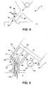
- Figure 4 shows the area of the insertion slot 20 in a side wall 18 of the receiving housing 6.
- the insertion slot 20 has a relatively long, straight portion, adjoined by a bent portion approximately parallel to the top of the punched grid 2.
- the end of the insertion slot 20 forms a lateral stop face 31 for a bearing journal to be described in more detail below, which bearing journal is centred on the swivel axis 14.
- the lateral stop face 31, the lower area of the end of the insertion slot 20 and the upper area, forming an upper limit stop 30, of the end of the insertion slot form a bearing journal seat 22.
- Figure 5 shows a partial sectional view at right angles to the swivel axis 14.
- the connector 10 here designated second connector is visible at the edge of the top of the punched grid 2 (the receiving housing 6 is not indicated in Figure 5).
- the second connector 10 has a second outer wall 102 located externally relative to the swivel axis 14, and a second inner wall 104, which forms with the second outer wall 102, a contact element-receiving chamber 48 in which a female (socket) contact element 106 is accommodated.
- the upper, inner ends of the second outer wall 102 and the second inner wall 104 project inwardly and thus protrude over the ends of the female contact element 106 in order to provide protection relative to the male blade contact element 40 to be inserted.
- the first connector 34 matching the second connector 10 is located on the lower end face of the printed circuit board 8, of which only the bottom end of the one side wall 12 is visible here.
- the first connector 34 has a first outer wall 36 located externally relative to the swivel axis 14, a first inner wall 38 and the above-mentioned blade contacts constituting the male contact elements 40.
- the inner end of the first outer wall 36 facing the swivel axis 14 is provided with a bevel 39.
- Figure 5 shows the situation after insertion of the printed circuit board 8 into the entry slots 20 and displacement of the printed circuit board into the preliminary catch position in accordance with the bent arrow P.
- the printed circuit board is guided in the insertion slots 20 during this process by the above-mentioned bearing journals.
- Figure 7 shows a partial sectional view of a bottom comer of the printed circuit board 8 with the side wall 12 fixed thereto, to whose outer bottom end there is fixed a bearing journal 24, whose end is terminated by a projecting flange 26. Together with a bearing journal located symmetrically at the other bottom end of the printed circuit board 8, the bearing journal 24 with its flange 26, illustrated in Figure 7, defines the swivel axis 14.
- the distance between the flange 26 and the outer side of the side wall 12 is only slightly larger than the thickness of the side wall 18 of the receiving housing 6, and the diameter of the bearing journal 24 is only slightly smaller than the width of the insertion slot 22, such that the printed circuit board 8 is guided with only minimal play when it is moved into the preliminary catch position.
- the tip of the bent arrow P corresponds to the preliminary catch position.
- the bottom edge in the area of the oblique face 39 of the first outer wall 36 meets the upper edge of the second outer wall 102 of the second connector 10. This prevents swivelling of the printed circuit board 8 before the preliminary catch position is reached.
- the preliminary catch position according to the illustration in Figure 5 has been reached, however, there is nothing to prevent the printed circuit board from swivelling.
- the left-hand upper edge of the second outer wall 102 of the second connector 10 touches the inner face of the first outer wall 36 in a slide guide area K1.
- Figure 5 shows that swivelling of the printed circuit board with the first connector 34 results in the tip of the blade contact 40 entering the insertion opening 50 and then the female (socket) contact element 106.
- Figure 6 shows the individual stages of the swivel connection process.
- Figure 6 shows that, during the majority of the swivel movement, the two outer walls 102, 36 of the connectors 10 and 34 touch at the slide guide area K1.
- the rounded surface zone b1 ( Figure 5) of the second inner wall 104 of the second connector 10 which second inner wall 104 is shorter than the second outer wall 102, makes it possible for the blade contact 40 to move past it reliably without collision.
- a bevel K2 on the inside of the first inner wall 38 of the first connector 34 prevents collision with the outer side of the second inner wall 104 of the second connector 10.
- the free end E1 of the first inner wall 38 of the first connector 34 is shorter than the end E2 of the first outer wall of this connector.
- Figure 8 shows the final situation after swivelling of the printed circuit board 8, which is then completely accommodated by the receiving housing 6.
- the above-described embodiment may be modified in many different ways.
- the insertion slots 25 do not have to take the form of through-slots in the side walls 18 of the receiving housing 6; instead, channels on the inside of the side walls 18 are also possible.
- the receiving housing 6 also does not need to be tall enough to accommodate the printed circuit board 8 completely.
- Male contact elements and female contact elements of the above embodiment may also occupy the opposite positions, i.e. the blade contacts 40 may be provided in the connector on the punched grid 2, while female contact elements are located in the other connector.
Landscapes
- Coupling Device And Connection With Printed Circuit (AREA)
Applications Claiming Priority (2)
| Application Number | Priority Date | Filing Date | Title |
|---|---|---|---|
| DE10359232 | 2003-12-17 | ||
| DE10359232A DE10359232A1 (de) | 2003-12-17 | 2003-12-17 | Leiterplatten-Steckverbindung |
Publications (1)
| Publication Number | Publication Date |
|---|---|
| EP1544957A1 true EP1544957A1 (en) | 2005-06-22 |
Family
ID=34485436
Family Applications (1)
| Application Number | Title | Priority Date | Filing Date |
|---|---|---|---|
| EP04028961A Withdrawn EP1544957A1 (en) | 2003-12-17 | 2004-12-07 | Printed circuit board plug-in connection |
Country Status (4)
| Country | Link |
|---|---|
| US (1) | US7101198B2 (enExample) |
| EP (1) | EP1544957A1 (enExample) |
| JP (1) | JP2005183380A (enExample) |
| DE (1) | DE10359232A1 (enExample) |
Cited By (4)
| Publication number | Priority date | Publication date | Assignee | Title |
|---|---|---|---|---|
| US7101198B2 (en) | 2003-12-17 | 2006-09-05 | Tyco Electronics Amp Gmbh | Printed circuit board plug-in connection |
| US9105997B2 (en) | 2010-08-27 | 2015-08-11 | Iriso Electronics Co., Ltd. | Connector |
| CN112261344A (zh) * | 2020-09-11 | 2021-01-22 | 安徽阿瑞斯科技有限公司 | 一种具有防护结构的内嵌5g模组的多功能会议机 |
| CN119581940A (zh) * | 2024-12-13 | 2025-03-07 | 镇江中铭电子有限公司 | 一种快速定位锁止的射频同轴连接器及其连接方法 |
Families Citing this family (3)
| Publication number | Priority date | Publication date | Assignee | Title |
|---|---|---|---|---|
| US7479020B2 (en) * | 2004-11-22 | 2009-01-20 | Visteon Global Technologies, Inc. | Electronic control module having an internal electric ground |
| CN103682816A (zh) * | 2013-11-25 | 2014-03-26 | 泰兴市航联电连接器有限公司 | 一种主动导向定位分离的电连接器 |
| JP6997127B2 (ja) * | 2019-03-26 | 2022-01-17 | ヒロセ電機株式会社 | コネクタ装置およびコネクタ |
Citations (2)
| Publication number | Priority date | Publication date | Assignee | Title |
|---|---|---|---|---|
| SU871264A1 (ru) * | 1980-01-03 | 1981-10-07 | Предприятие П/Я А-1335 | Многоконтактный электрический разъем |
| US5476392A (en) * | 1993-04-19 | 1995-12-19 | Yazaki Corporation | Connector device |
Family Cites Families (6)
| Publication number | Priority date | Publication date | Assignee | Title |
|---|---|---|---|---|
| US4972296A (en) * | 1989-06-15 | 1990-11-20 | Northern Telecom Limited | Expandable modular switching unit |
| GB9127466D0 (en) | 1991-12-30 | 1992-02-19 | Amp Gmbh | Electronic control module assembly |
| JPH11283699A (ja) * | 1998-03-31 | 1999-10-15 | Yazaki Corp | コネクタ構造 |
| FR2782577B1 (fr) * | 1998-08-24 | 2000-11-17 | Framatome Connectors Int | Connecteur avec fiche et embase a faible force d'insertion, notamment du type a contacts broche/lyre |
| US6676430B1 (en) * | 2000-05-23 | 2004-01-13 | Avaya Technology Corp. | Board mounted jack module |
| DE10359232A1 (de) | 2003-12-17 | 2005-07-21 | Tyco Electronics Amp Gmbh | Leiterplatten-Steckverbindung |
-
2003
- 2003-12-17 DE DE10359232A patent/DE10359232A1/de not_active Ceased
-
2004
- 2004-12-07 EP EP04028961A patent/EP1544957A1/en not_active Withdrawn
- 2004-12-10 JP JP2004358794A patent/JP2005183380A/ja not_active Withdrawn
- 2004-12-13 US US11/010,582 patent/US7101198B2/en not_active Expired - Fee Related
Patent Citations (2)
| Publication number | Priority date | Publication date | Assignee | Title |
|---|---|---|---|---|
| SU871264A1 (ru) * | 1980-01-03 | 1981-10-07 | Предприятие П/Я А-1335 | Многоконтактный электрический разъем |
| US5476392A (en) * | 1993-04-19 | 1995-12-19 | Yazaki Corporation | Connector device |
Non-Patent Citations (1)
| Title |
|---|
| DATABASE WPI Section EI Week 198231, Derwent World Patents Index; Class V04, AN 1982-K4132E, XP002314363, "Hinged multiple-contact electric connector - has housings of contact elements hinged relative to one another with rotation axis on contact axis" * |
Cited By (5)
| Publication number | Priority date | Publication date | Assignee | Title |
|---|---|---|---|---|
| US7101198B2 (en) | 2003-12-17 | 2006-09-05 | Tyco Electronics Amp Gmbh | Printed circuit board plug-in connection |
| US9105997B2 (en) | 2010-08-27 | 2015-08-11 | Iriso Electronics Co., Ltd. | Connector |
| CN112261344A (zh) * | 2020-09-11 | 2021-01-22 | 安徽阿瑞斯科技有限公司 | 一种具有防护结构的内嵌5g模组的多功能会议机 |
| CN112261344B (zh) * | 2020-09-11 | 2022-10-25 | 安徽阿瑞斯科技有限公司 | 一种具有防护结构的内嵌5g模组的多功能会议机 |
| CN119581940A (zh) * | 2024-12-13 | 2025-03-07 | 镇江中铭电子有限公司 | 一种快速定位锁止的射频同轴连接器及其连接方法 |
Also Published As
| Publication number | Publication date |
|---|---|
| US7101198B2 (en) | 2006-09-05 |
| JP2005183380A (ja) | 2005-07-07 |
| US20050153579A1 (en) | 2005-07-14 |
| DE10359232A1 (de) | 2005-07-21 |
Similar Documents
| Publication | Publication Date | Title |
|---|---|---|
| US7448888B2 (en) | Connector and a connector assembly | |
| CN107799938B (zh) | 电连接器以及连接器装置 | |
| EP1180827B1 (en) | Lever type connector | |
| US6592404B2 (en) | Half fit preventive connector | |
| EP0272804A1 (en) | Mounting means and method for rack and panel connector | |
| US6716069B2 (en) | Connector with a housing and a retainer held securely on the housing | |
| KR20170068389A (ko) | 커넥터 장치 | |
| EP1962390B1 (en) | A connector and a connector assembly | |
| JPH0917505A (ja) | 嵌合保証装置付コネクタ組立体、それに使用されるコネクタ及びその嵌合保証装置 | |
| EP0905823B1 (en) | Electrical connector | |
| EP0510229A1 (en) | An electrical connector with positive latch | |
| US5402320A (en) | Electronic shelf keying and alignment combination | |
| US7101198B2 (en) | Printed circuit board plug-in connection | |
| US20060281374A1 (en) | Electrical Connector | |
| EP0713263B1 (en) | Self-locking mating terminal structure | |
| US9559460B2 (en) | Lever-type connector with regulating protrusion on male housing that engages lever on female housing to achieve connection without inclination between male and female housings | |
| EP0797274B1 (en) | Connector connecting structure | |
| US8337255B2 (en) | Connector and series of connectors | |
| US6220886B1 (en) | Connector | |
| GB2393045A (en) | Connector structure | |
| EP1150388B1 (en) | A shake preventing construction for a terminal fitting and connector | |
| JP7307006B2 (ja) | シールド電気コネクタ | |
| EP1176671A1 (en) | An electrical connector | |
| US6007354A (en) | Connector fitting structure and fitting method using the same | |
| CN115332857B (zh) | 连接器 |
Legal Events
| Date | Code | Title | Description |
|---|---|---|---|
| PUAI | Public reference made under article 153(3) epc to a published international application that has entered the european phase |
Free format text: ORIGINAL CODE: 0009012 |
|
| AK | Designated contracting states |
Kind code of ref document: A1 Designated state(s): AT BE BG CH CY CZ DE DK EE ES FI FR GB GR HU IE IS IT LI LT LU MC NL PL PT RO SE SI SK TR |
|
| AX | Request for extension of the european patent |
Extension state: AL BA HR LV MK YU |
|
| 17P | Request for examination filed |
Effective date: 20051208 |
|
| AKX | Designation fees paid |
Designated state(s): DE FR GB IT |
|
| STAA | Information on the status of an ep patent application or granted ep patent |
Free format text: STATUS: THE APPLICATION IS DEEMED TO BE WITHDRAWN |
|
| 18D | Application deemed to be withdrawn |
Effective date: 20100701 |