EP1544161A1 - Three-dimensional structure element and method of manufacturing the element, optical switch, and micro device - Google Patents
Three-dimensional structure element and method of manufacturing the element, optical switch, and micro device Download PDFInfo
- Publication number
- EP1544161A1 EP1544161A1 EP03766675A EP03766675A EP1544161A1 EP 1544161 A1 EP1544161 A1 EP 1544161A1 EP 03766675 A EP03766675 A EP 03766675A EP 03766675 A EP03766675 A EP 03766675A EP 1544161 A1 EP1544161 A1 EP 1544161A1
- Authority
- EP
- European Patent Office
- Prior art keywords
- substrate
- dummy
- area
- structures
- dimensional
- Prior art date
- Legal status (The legal status is an assumption and is not a legal conclusion. Google has not performed a legal analysis and makes no representation as to the accuracy of the status listed.)
- Granted
Links
Images




Classifications
-
- B—PERFORMING OPERATIONS; TRANSPORTING
- B81—MICROSTRUCTURAL TECHNOLOGY
- B81B—MICROSTRUCTURAL DEVICES OR SYSTEMS, e.g. MICROMECHANICAL DEVICES
- B81B7/00—Microstructural systems ; Auxiliary parts of microstructural devices or systems
- B81B7/04—Networks or arrays of similar microstructural devices
-
- B—PERFORMING OPERATIONS; TRANSPORTING
- B81—MICROSTRUCTURAL TECHNOLOGY
- B81B—MICROSTRUCTURAL DEVICES OR SYSTEMS, e.g. MICROMECHANICAL DEVICES
- B81B3/00—Devices comprising flexible or deformable elements, e.g. comprising elastic tongues or membranes
- B81B3/0064—Constitution or structural means for improving or controlling the physical properties of a device
- B81B3/0067—Mechanical properties
- B81B3/0072—For controlling internal stress or strain in moving or flexible elements, e.g. stress compensating layers
-
- B—PERFORMING OPERATIONS; TRANSPORTING
- B81—MICROSTRUCTURAL TECHNOLOGY
- B81C—PROCESSES OR APPARATUS SPECIALLY ADAPTED FOR THE MANUFACTURE OR TREATMENT OF MICROSTRUCTURAL DEVICES OR SYSTEMS
- B81C1/00—Manufacture or treatment of devices or systems in or on a substrate
-
- G—PHYSICS
- G02—OPTICS
- G02B—OPTICAL ELEMENTS, SYSTEMS OR APPARATUS
- G02B26/00—Optical devices or arrangements for the control of light using movable or deformable optical elements
- G02B26/02—Optical devices or arrangements for the control of light using movable or deformable optical elements for controlling the intensity of light
-
- G—PHYSICS
- G02—OPTICS
- G02B—OPTICAL ELEMENTS, SYSTEMS OR APPARATUS
- G02B26/00—Optical devices or arrangements for the control of light using movable or deformable optical elements
- G02B26/08—Optical devices or arrangements for the control of light using movable or deformable optical elements for controlling the direction of light
-
- G—PHYSICS
- G02—OPTICS
- G02B—OPTICAL ELEMENTS, SYSTEMS OR APPARATUS
- G02B6/00—Light guides; Structural details of arrangements comprising light guides and other optical elements, e.g. couplings
- G02B6/24—Coupling light guides
- G02B6/26—Optical coupling means
- G02B6/35—Optical coupling means having switching means
- G02B6/351—Optical coupling means having switching means involving stationary waveguides with moving interposed optical elements
- G02B6/3512—Optical coupling means having switching means involving stationary waveguides with moving interposed optical elements the optical element being reflective, e.g. mirror
- G02B6/3518—Optical coupling means having switching means involving stationary waveguides with moving interposed optical elements the optical element being reflective, e.g. mirror the reflective optical element being an intrinsic part of a MEMS device, i.e. fabricated together with the MEMS device
-
- B—PERFORMING OPERATIONS; TRANSPORTING
- B81—MICROSTRUCTURAL TECHNOLOGY
- B81C—PROCESSES OR APPARATUS SPECIALLY ADAPTED FOR THE MANUFACTURE OR TREATMENT OF MICROSTRUCTURAL DEVICES OR SYSTEMS
- B81C2201/00—Manufacture or treatment of microstructural devices or systems
- B81C2201/01—Manufacture or treatment of microstructural devices or systems in or on a substrate
- B81C2201/0101—Shaping material; Structuring the bulk substrate or layers on the substrate; Film patterning
- B81C2201/0102—Surface micromachining
- B81C2201/0105—Sacrificial layer
- B81C2201/0108—Sacrificial polymer, ashing of organics
-
- G—PHYSICS
- G02—OPTICS
- G02B—OPTICAL ELEMENTS, SYSTEMS OR APPARATUS
- G02B6/00—Light guides; Structural details of arrangements comprising light guides and other optical elements, e.g. couplings
- G02B6/24—Coupling light guides
- G02B6/26—Optical coupling means
- G02B6/35—Optical coupling means having switching means
- G02B6/354—Switching arrangements, i.e. number of input/output ports and interconnection types
- G02B6/3544—2D constellations, i.e. with switching elements and switched beams located in a plane
- G02B6/3546—NxM switch, i.e. a regular array of switches elements of matrix type constellation
-
- G—PHYSICS
- G02—OPTICS
- G02B—OPTICAL ELEMENTS, SYSTEMS OR APPARATUS
- G02B6/00—Light guides; Structural details of arrangements comprising light guides and other optical elements, e.g. couplings
- G02B6/24—Coupling light guides
- G02B6/26—Optical coupling means
- G02B6/35—Optical coupling means having switching means
- G02B6/3564—Mechanical details of the actuation mechanism associated with the moving element or mounting mechanism details
- G02B6/3568—Mechanical details of the actuation mechanism associated with the moving element or mounting mechanism details characterised by the actuating force
- G02B6/3572—Magnetic force
-
- G—PHYSICS
- G02—OPTICS
- G02B—OPTICAL ELEMENTS, SYSTEMS OR APPARATUS
- G02B6/00—Light guides; Structural details of arrangements comprising light guides and other optical elements, e.g. couplings
- G02B6/24—Coupling light guides
- G02B6/26—Optical coupling means
- G02B6/35—Optical coupling means having switching means
- G02B6/3564—Mechanical details of the actuation mechanism associated with the moving element or mounting mechanism details
- G02B6/3584—Mechanical details of the actuation mechanism associated with the moving element or mounting mechanism details constructional details of an associated actuator having a MEMS construction, i.e. constructed using semiconductor technology such as etching
-
- G—PHYSICS
- G02—OPTICS
- G02B—OPTICAL ELEMENTS, SYSTEMS OR APPARATUS
- G02B6/00—Light guides; Structural details of arrangements comprising light guides and other optical elements, e.g. couplings
- G02B6/24—Coupling light guides
- G02B6/26—Optical coupling means
- G02B6/35—Optical coupling means having switching means
- G02B6/3596—With planar waveguide arrangement, i.e. in a substrate, regardless if actuating mechanism is outside the substrate
-
- Y—GENERAL TAGGING OF NEW TECHNOLOGICAL DEVELOPMENTS; GENERAL TAGGING OF CROSS-SECTIONAL TECHNOLOGIES SPANNING OVER SEVERAL SECTIONS OF THE IPC; TECHNICAL SUBJECTS COVERED BY FORMER USPC CROSS-REFERENCE ART COLLECTIONS [XRACs] AND DIGESTS
- Y10—TECHNICAL SUBJECTS COVERED BY FORMER USPC
- Y10S—TECHNICAL SUBJECTS COVERED BY FORMER USPC CROSS-REFERENCE ART COLLECTIONS [XRACs] AND DIGESTS
- Y10S438/00—Semiconductor device manufacturing: process
- Y10S438/926—Dummy metallization
Definitions
- the present invention relates to an element having a three-dimensional structure that is formed accurately on a substrate such as a silicon wafer using a sacrificial layer and a method of manufacturing the element.
- the invention relates to an optical switch that is formed using a sacrificial layer and a method of manufacturing the optical switch.
- a method of forming a sacrificial layer on a substrate such as a silicon wafer, forming a thin film structure patterned in a desired shape on the sacrificial layer, and thereafter forming a desired three-dimensional structure by removing the sacrificial layer has been attracting attentions. Since it is possible to form a large number of fine three-dimensional structures accurately and at a high density with this method, the method is suitable for manufacturing a spatial light modulation element and the like.
- Japanese Patent Laid-open Publication No. 2001-13426 and Japanese Patent Laid-open Publication No. 2001-129798 disclose use of a solution for wet etching such as a hydrofluoric acid water solution.
- a solution for wet etching such as a hydrofluoric acid water solution.
- the solution for etching like the hydrofluoric acid water solution that uses water as a solvent, a phenomenon in which water molecules adhere to the thin film structure at the time of etching and the thin film structure adheres to the substrate due to a surface tension of the water molecules tends to occur.
- the thin film structure may keep adhering to the substrate after a dry process to make it impossible to obtain a desired three-dimensional shape.
- a thin film structure of a three-dimensional shape including a movable portion is formed, if the thin film structure adheres to a substrate, a function of the movable portion cannot be performed.
- a method of removing a sacrificial layer with a dry process such as ashing has been proposed.
- a dry process such as ashing
- an organic resist film is used as the sacrificial layer.
- temperature reaches as high as several hundred degrees at the time of the ashing in the area where only the sacrificial layer is exposed on the substrate, temperature does not rise to such high temperature in the area where the sacrificial layer is sandwiched between the thin film structure and the substrate.
- the temperature may be higher than substrate temperature at the time of formation of the thin film structure and heat treatment temperature.
- the sacrificial layer is sandwiched between the thin film structure and the substrate, temperature does not rise to such high temperature.
- a three-dimensional structure element as described below is provided.
- the present invention provides a three-dimensional structure element including: a substrate; andthree-dimensional structures arranged in a predetermined effective area on the substrate, wherein the three-dimensional structures have space portions, which are formed by removing a sacrificial layer, between the three-dimensional structures and the substrate, and on the substrate, a dummy area is arranged to surround the effective area, dummy structures are arranged in the dummy area, and the dummy structures have space portions, which are formed by removing a sacrificial layer, between the dummy structures and the substrate.
- the three-dimensional structure element it is possible to form a portion of the dummy structures opposed to the substrate in the same shape as the three-dimensional structures.
- the dummy structures in a configuration having columns for fixing at least one section thereof to the substrate.
- the dummy structures in a configuration having a thin film covering the dummy area and plural columns arranged between the thin film and the substrate.
- an optical switch as described below is provided.
- the present invention provides an optical switch including: an optical waveguide substrate; and a three-dimensional element substrate including displaceable reflecting mirrors, wherein the three-dimensional structure element substrate has a substrate and three-dimensional structures arranged in a predetermined effective area on the substrate, the three-dimensional structures have the reflecting mirrors and displacement portions on which the reflecting mirrors are placed, and the displacement portions have space portions, which are formed by removing a sacrificial layer, between the displacement portions and the substrate, and on the substrate, a dummy area is arranged to surround the effective area, dummy structures are arranged in the dummy area, and the dummy structures have space portions, which are formed by removing a sacrificial layer, between the dummy structures and the substrate.
- micro device as described below is provided.
- the present invention provides a micro device including displaceable thin film three-dimensional structures, characterized in that the micro device has a substrate and the thin film three-dimensional structures arranged in a predetermined effective area on the substrate, the thin film three-dimensional structures have space portions, which are formed by removing a sacrificial layer, between the thin film three-dimensional structures and the substrate, and on the substrate, a dummy area is arranged to surround the effective area, dummy structures made of a thin film are arranged in the dummy area, and the dummy structures have space portions, which are formed by removing a sacrificial layer, between the dummy structures and the substrate.
- a method of manufacturing a three-dimensional structure element as described below is provided.
- the present invention provides a method of manufacturing a three-dimensional structure element including:
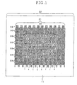
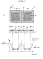
- a three-dimensional structure element includes a substrate 11, an effective area 20 provided in the center of the substrate 11, a dummy area 21 surrounding the effective area 20, and an ineffective area 22 around the dummy area 21.
- plural three-dimensional structures 1 are arranged, that is, sixteen three-dimensional structures 1 are arranged vertically and horizontally, respectively (16 ⁇ 16 three-dimensional structures 1) (in Fig. 1, for convenience of illustration, eight three-dimensional structures 1 are arranged vertically and horizontally, respectively).
- the three-dimensional structure 1 has a displacement portion 13 of a cantilever shape and a reflecting mirror 2 placed at one end of the displacement portion 13.
- the displacement portion 13 has a configuration in which two thin films of different materials are stacked and has two legs 52 at ends on the opposite side of an end where the reflecting mirror 2 is placed. The two legs 52 are fixed to the substrate 11.
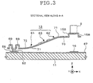
- the displacement portion 13 In a state in which no force is applied from the outside, the displacement portion 13 is bent as shown in Fig. 3 by an internal stress of the thin films forming the displacement portion 13 to come into a state in which the displacement portion 13 lifts the reflecting mirror 2 to a position apart from the substrate 11.
- a not-shown wiring pattern layer is formed in the displacement portion 13.
- a wiring pattern layer 58 On the substrate 11, a wiring pattern layer 58 is arranged in a position, where the legs 52 of the displacement portion 13 are in contact with the substrate 11, and electrically connected to the wiring pattern layer of the displacement portion 13 to feed an electric current to the wiring pattern layer of the displacement portion 13.
- a wiring pattern layer 16 for generating a magnetic field is arranged in a portion on the substrate 11 and below the reflecting mirror 2.
- an electric current is fed to the wiring pattern layer of the displacement portion 13 and an electric current is fed to the wiring pattern layer 16 to generate a magnetic field, whereby it is possible to draw the displacement portion 13 toward the substrate 11 with the Lorentz force and lower the reflecting mirror 2 to the position of the substrate 11.
- plural dummy structures 33 are arranged in the dummy area 21 on the substrate 11. These dummy structures 33 are arranged to prevent the dummy area 21 from being heated to high temperature in a process of removing a sacrificial layer in a manufacturing method to be described later.
- the dummy structures 33 are formed in the same shape as the displacement portions 13 of the three-dimensional structures 1 and have legs 352 that are the same as the legs 52 of the displacement portions 13.
- the dummy structures 33 are arranged vertically and horizontally at the same pitch as the three-dimensional structures 1 in the effective area 20.
- the reflecting mirrors 2 and the wiring pattern layers are not formed in the dummy structures 33 in order to simplify a configuration thereof. Note that, in Fig.
- Fig. 1 shows shapes of upper surfaces of the three-dimensional structures 1 and the dummy structures 33.
- the three-dimensional structures 1 and the dummy structures 33 are not arranged in the ineffective area 22 on the substrate 11.
- wiring pattern layers 58 and 16 are arranged for drawing around wiring.
- a wafer-like silicon substrate is used as the substrate 11, a large number of the three-dimensional structure elements in Fig. 1 are arranged two-dimensionally, and finally cut out to complete the three-dimensional structure elements.
- Figs. 6A to 6G to be referred to in the following explanation, only a sectional part of one three-dimensional structure 1 of one three-dimensional structure element is shown. However, treatments such as the film formation, the photolithography, and the etching are applied to the entire wafer-like substrate 11.
- a silicon oxide film 57 is formed over an entire upper surface of the wafer-like substrate 11 by a thermal oxidation method, an Al film to be the wiring pattern layer 58 and the wiring pattern layer 16 is formed on the silicon oxide film 57, and by the photolithography and etching, the Al film is patterned into respective shapes of the wiring pattern layer 58 and the wiring pattern layer 16 (Fig. 6A).
- a resist layer to be a sacrificial layer 80 is formed over the entire upper surface of the wafer-like substrate 11 in this state by application and baking, and an opening 80a is formed in a position to be the legs 52 by the photolithography and the etching (Fig. 6(b)).
- a resist layer 81 to be a sacrificial layer is formed over the entire surface of the wafer-like substrate 11 in the state shown in Fig. 6 (b) by application and baking, and the resist layer 81 is left in a predetermined shape, for example, an island shape around the positions of the legs 52 and in a position where the reflecting mirror 2 is placed, by the photolithography and the etching (Fig. 6(c)).
- This left sacrificial layer 81 is arranged in order to form steps 59 and 158 in the displacement portion 13 as shown in Fig. 3. It is possible to increase strength of the displacement portion 13 by forming the steps 59 and 158.
- the displacement portions 13 and the legs 52 are formed in the effective area 20 using an Al film 73, an SiN film 71, and an Al film 72 and the dummy structures 33 having the same structure as the displacement portion 13 are formed in the dummy area 21.
- the displacement portion 13 is formed to be made up of three portions, namely, a base 61 warped upward, a tip portion 62 warped downward, and a connecting portion 63 connecting the base 61 and the tip portion 62.
- the directions of the warps of the base 61 and the tip portion 62 are set to be opposite in this way, whereby, even if a distance from the leg 52 to the tip of the displacement portion 13 is long, it is possible to reduce a space between the tip and the substrate 11. Consequently, it is possible to switch a position where the reflecting mirror 2 is lifted to a position where the reflecting mirror 2 is drawn toward the substrate 11, by a small Lorentz force.
- the base 61 has a configuration in which the SiN film 71 and the Al film 72 are stacked from the base 11 side.
- the tip portion 62 has a configuration in which the Al film 73 and the SiN film 71 are stacked from the base 11 side.
- the connecting portion 63 is constituted such that these films overlap partially.
- the legs 52 are formed integrally with the base 61. Note that, when the Al films 73 and 72 and the SiN film 71 are formed, the substrate 11 is heated to a predetermined temperature in order to control internal stresses of the respective films.
- the SiN film is patterned by the photolithography and the etching to have shapes of the base 61, the legs 52, and the tip portion 62 of the displacement portion 13 and the dummy structure 33 (Fig. 6(e)).
- an opening is provided in the SiN film 71 in a position of a bottom of the opening 80a to be the legs 52. Consequently, the Al film 72 and the wiring pattern layer 58 to be formed next are connected.
- the Al film is patterned to have shapes of the base 61, the legs 52, and the connecting portion 63 of the displacement portion 13 and the dummy structure 33 (Fig. 6(f)).
- the displacement portion 13 and the legs 52 having a shape, in which the Al film 72 of the base 61 and the Al film 73 of the tip portion 62 overlap in the connecting portion 63, are formed.
- a resist layer to be the sacrificial layer 82 is applied thick over the entire wafer-like substrate 11 and baked, an opening of a shape of the reflecting mirror 2 is formed by exposure and development in a position where the reflecting mirror 2 should be formed. Thereafter, Au, Ni, or another metal is grown by electrolytic plating to fill the opening. Consequently, the reflecting mirror 2 is formed.
- the portions of the effective areas 20 and the dummy area 21 have a structure in which the displacement portion 13 and the dummy structure 33 are sandwiched between the sacrifice layer 80 and the sacrifice layer 82.
- the portion of the ineffective area 22 has a structure in which the sacrificial layer 80 and the sacrificial layer 82 are stacked directly.
- groove-like slits are formed in boundaries of the respective three-dimensional structure elements of the wafer-like substrate 11 by dicing or the like.
- the slits do not completely cut the substrate 11 but is formed in a shape of a groove.
- the substrate 11 maintains the wafer shape.
- the sacrificial layer 80, the sacrificial layer 82, and the sacrificial layer 81 are removed by plasma ashing. Consequently, the displacement portion 13 in the effective area 20 and the dummy structure 33 in the dummy area 21 stand from the substrate 11 to form a three-dimensional structure as shown in Fig. 3.
- the plasma reacts with the sacrificial layers 80 and 81 while gradually invading from gaps of the displacement portion 13 and the dummy structure 33.
- a reaction rate of the effective area 20 and the dummy area 21 is low compared with that of the ineffective area 22, and temperature of the effective area 20 and the dummy area 21 does not rise to high temperature like that of the ineffective area 22.
- temperature of the ineffective area 22 rose to high temperature of several hundred degrees, which was higher than a substrate temperature at the time of formation of the Al films 73 and 72 and the SiN film 71 constituting the displacement portion 13.
- temperature of the effective area 20 and the dummy area 21 was lower than the substrate temperature at the time of formation of the films.
- a width of the dummy area 21 is kept at a width of about 500 ⁇ m. By giving a width of this level to the dummy area 21, heat generated in the ineffective area 22 is prevented from being conducted to the effective area 20 significantly.
- the method of removing a sacrificial layer is not limited to the plasma ashing, and it is also possible to use ion ashing, dry etching, and the like. In this case, it is also possible to prevent heat of reaction of an ineffective area from being conducted to an effective area by providing a dummy area in a boundary cf the effective area and the ineffective area.
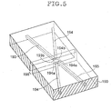
- an optical switch by superimposing the three-dimensional structure element of this embodiment on an optical waveguide substrate 190 in which plural optical waveguides such as optical waveguides 193 and 194 are formed as shown in Fig. 5. Although only a part of the optical waveguide substrate 190 is shown in Fig. 5, a large number of optical waveguides such as the optical waveguides 193 and 194 are arranged in the optical waveguide substrate 190 to cross in a diamond lattice shape at fixed intervals, and a groove 196 is formed to traverse a point where the optical waveguides intersect.
- a pitch of the 16 ⁇ 16 three-dimensional structures 1 arranged on the substrate is defined to coincide with the intervals of the points where the optical waveguides of the optical waveguide substrate 190 intersect.
- the dummy structure 33 is formed in the stacked structure of the Al films 73 and 72 and the SiN film 71 in the same manner as the displacement portion 13.
- the dummy structure 33 since the dummy structure 33 only has to set a reaction rate of the dummy area 21 at the time of the ashing to the same level as a reaction rate of the effective area 20, it is possible to constitute the dummy structure 33 with any one of the layers.
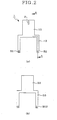
- a pattern shape of the dummy structure does not have to be the same as that of the displacement portion 13. It is possible to form the dummy structure in a shape in which several displacement portions 13 of the three-dimensional structure 1 are continuously formed as in the dummy structure 34 shown in Figs. 8A and 8B and form the dummy structure in a size larger than the displacement portion 13.
- columns 35 for fixing the substrate 11 are formed in plural places in the peripheral portion of the dummy structure 34.
- the columns 35 have the same configuration as the legs 52 of the displacement portion 13 and can be formed integrally with thin films constituting the dummy structure 34.
- the dummy structure 34 has an action of substantially equalizing an ashing rate of the dummy area 21 with the ashing rate in the effective area 20.
- a width of the dummy area is also set to 500 ⁇ m.
- a dummy structure 36 in Fig. 9 the entire dummy area 21 in the peripheral portion of the effective area 20 is covered by one continuous thin film. Consequently, an ashing rate of the dummy area 21 is set smaller than that of the ineffective area 22.
- the plural columns 35 are also arranged at fixed intervals to prevent the dummy structure 36 from sticking to the substrate 11 at the time of the ashing or curling up to make the sacrificial layer 80 on the substrate 11 side easily subjected to the ashing.
- a width of the dummy area 22 is set to about 1 mm.
- a shape of a dummy structure formed in the dummy area 21 is not limited, and any shape may be adopted as long as the dummy structure can cover the sacrificial layer 80 to thereby set an ashing rate of the dummy area 21 smaller than that of the ineffective area22.
- a shape and a dimension of the dummy area 21 freely.
- the dummy area 21 including dummy structures is arranged to be in contact with the outer side of the effective area 20, temperature of the dummy area 21 does nor rise to high temperature compared with the ineffective area 22 even during the ashing process and is not largely different from temperature in the effective area.
- the three-dimensional structure elements 1 in the effective area 20 after completion there is no distribution in a residual stress, and amounts of distortion of the three-dimensional structure elements 1 after removing a sacrificial layer are uniform.
- an optical switch using such a three-dimensional structure element, it is possible to control plural switching mechanisms with substantially the same control signal.
- the three-dimensional structure element in which the 16 ⁇ 16 three-dimensional structures 1 are arranged two-dimensionally in the effective area 20, is described as a three-dimensional structure element.
- the number of three-dimensional structures and an arrangement thereof are not limited to this configuration.
- the present invention is also effective for a shape in which one three-dimensional structure is arranged for the entire effective area 20.
- a micro device other than the optical switch such as an infrared ray sensor or a digital mirror device, using a three-dimensional structure element including a three-dimensional structure of a desired shape.
- a three-dimensional structure element including plural three-dimensional structures, in a configuration that the three-dimensional structures can be formed uniformly without causing fluctuation in a shape of the three-dimensional structures.
Landscapes
- Physics & Mathematics (AREA)
- Engineering & Computer Science (AREA)
- General Physics & Mathematics (AREA)
- Optics & Photonics (AREA)
- Microelectronics & Electronic Packaging (AREA)
- Computer Hardware Design (AREA)
- Mechanical Engineering (AREA)
- Manufacturing & Machinery (AREA)
- Micromachines (AREA)
- Mechanical Light Control Or Optical Switches (AREA)
Abstract
Description
the three-dimensional structures have space portions, which are formed by removing a sacrificial layer, between the three-dimensional structures and the substrate, and
on the substrate, a dummy area is arranged to surround the effective area, dummy structures are arranged in the dummy area, and the dummy structures have space portions, which are formed by removing a sacrificial layer, between the dummy structures and the substrate.
the three-dimensional structure element substrate has a substrate and three-dimensional structures arranged in a predetermined effective area on the substrate,
the three-dimensional structures have the reflecting mirrors and displacement portions on which the reflecting mirrors are placed, and the displacement portions have space portions, which are formed by removing a sacrificial layer, between the displacement portions and the substrate, and
on the substrate, a dummy area is arranged to surround the effective area, dummy structures are arranged in the dummy area, and the dummy structures have space portions, which are formed by removing a sacrificial layer, between the dummy structures and the substrate.
the micro device has a substrate and the thin film three-dimensional structures arranged in a predetermined effective area on the substrate,
the thin film three-dimensional structures have space portions, which are formed by removing a sacrificial layer, between the thin film three-dimensional structures and the substrate, and
on the substrate, a dummy area is arranged to surround the effective area, dummy structures made of a thin film are arranged in the dummy area, and the dummy structures have space portions, which are formed by removing a sacrificial layer, between the dummy structures and the substrate.
Claims (7)
- A three-dimensional structure element comprising:a substrate; andthree-dimensional structures arranged in a predetermined effective area on the substrate, wherein
the three-dimensional structures have space portions, which are formed by removing a sacrificial layer, between the three-dimensional structures and the substrate, and
on the substrate, a dummy area is arranged to surround the effective area, dummy structures are arranged in the dummy area, and the dummy structures have space portions, which are formed by removing a sacrificial layer, between the dummy structures and the substrate. - A three-dimensional structure element according to claim 1, wherein a portion of the dummy structures opposed to the substrate is formed in a same shape as the three-dimensional structures.
- A three-dimensional structure element according to claim 1, wherein the dummy structures have columns for fixing at least one section thereof to the substrate.
- A three-dimensional structure element according to claim 1, wherein the dummy structures have a thin film covering the dummy area and plural columns arranged between the thin film and the substrate.
- An optical switch comprising:an optical waveguide substrate; anda three-dimensional element substrate including displaceable reflecting mirrors, whereinthe three-dimensional structure element substrate has a substrate and three-dimensional structures arranged in a predetermined effective area on the substrate,the three-dimensional structures include the reflecting mirrors and displacement portions on which the reflecting mirrors are placed, and the displacement portions have space portions, which are formed by removing a sacrificial layer, between the displacement portions and the substrate, andon the substrate, a dummy area is provided to surround the effective area, dummy structures are arranged in the dummy area, and the dummy structures have space portions, which are formed by removing a sacrificial layer, between the dummy structures and the substrate.
- A micro device comprising displaceable thin film three-dimensional structures, whereinthe micro device has a substrate and the thin film three-dimensional structures arranged in a predetermined effective area on the substrate,the thin film three-dimensional structures have space portions, which are formed by removing a sacrificial layer, between the thin film three-dimensional structures and the substrate, andon the substrate, a dummy area is arranged to surround the effective area, dummy structures made of a thin film are arranged in the dummy area, and the dummy structures have space portions, which are formed by removing a sacrificial layer, between the dummy structures and the substrate.
- A method of manufacturing a three-dimensional structure element comprising:a step of forming a sacrificial layer and predetermined thin film three-dimensional structures in a predetermined effective area on a substrate and forming a sacrificial layer and predetermined thin film dummy structures in a dummy area surrounding the effective area; anda step of removing the sacrificial layers in the effective area and the dummy area with a dry process.
Applications Claiming Priority (3)
| Application Number | Priority Date | Filing Date | Title |
|---|---|---|---|
| JP2002224530A JP4300766B2 (en) | 2002-08-01 | 2002-08-01 | Three-dimensional structure element and manufacturing method thereof, optical switch, and microdevice |
| JP2002224530 | 2002-08-01 | ||
| PCT/JP2003/009734 WO2004013037A1 (en) | 2002-08-01 | 2003-07-31 | Three-dimensional structure element and method of manufacturing the element, optical switch, and micro device |
Publications (3)
| Publication Number | Publication Date |
|---|---|
| EP1544161A1 true EP1544161A1 (en) | 2005-06-22 |
| EP1544161A4 EP1544161A4 (en) | 2005-11-02 |
| EP1544161B1 EP1544161B1 (en) | 2009-01-14 |
Family
ID=31492130
Family Applications (1)
| Application Number | Title | Priority Date | Filing Date |
|---|---|---|---|
| EP03766675A Expired - Lifetime EP1544161B1 (en) | 2002-08-01 | 2003-07-31 | Three-dimensional structure element and method of manufacturing the element, optical switch, and micro device |
Country Status (9)
| Country | Link |
|---|---|
| US (1) | US7298015B2 (en) |
| EP (1) | EP1544161B1 (en) |
| JP (1) | JP4300766B2 (en) |
| KR (1) | KR101001123B1 (en) |
| CN (1) | CN1671617A (en) |
| AU (1) | AU2003252755A1 (en) |
| DE (1) | DE60325869D1 (en) |
| TW (1) | TWI274185B (en) |
| WO (1) | WO2004013037A1 (en) |
Cited By (2)
| Publication number | Priority date | Publication date | Assignee | Title |
|---|---|---|---|---|
| WO2008036959A3 (en) * | 2006-09-22 | 2009-02-26 | Stereo Display Inc | Micromirror array device comprising encapsulated reflective metal layer and method of making the same |
| EP3715932A4 (en) * | 2017-11-24 | 2021-08-18 | Hamamatsu Photonics K.K. | SLICE |
Families Citing this family (7)
| Publication number | Priority date | Publication date | Assignee | Title |
|---|---|---|---|---|
| KR100827314B1 (en) * | 2005-10-10 | 2008-05-06 | 삼성전기주식회사 | Method of manufacturing MEMS element and optical modulator having flat surface by heat treatment |
| DE102008001663B4 (en) * | 2008-05-08 | 2017-11-02 | Robert Bosch Gmbh | Micromechanical component and production method for a micromechanical component |
| WO2010122879A1 (en) * | 2009-04-23 | 2010-10-28 | コニカミノルタホールディングス株式会社 | Light reflection mechanism, optical interferometer and spectral analyzer |
| JP7131901B2 (en) | 2017-11-24 | 2022-09-06 | 浜松ホトニクス株式会社 | Transportation method |
| JP6902571B2 (en) * | 2017-11-24 | 2021-07-14 | 浜松ホトニクス株式会社 | Wafer |
| JP7025903B2 (en) * | 2017-11-24 | 2022-02-25 | 浜松ホトニクス株式会社 | Electrical inspection method |
| DE102020205189A1 (en) | 2020-04-23 | 2021-10-28 | Robert Bosch Gesellschaft mit beschränkter Haftung | Cap device, cap wafer and micromechanical packaging |
Family Cites Families (26)
| Publication number | Priority date | Publication date | Assignee | Title |
|---|---|---|---|---|
| US5636070A (en) * | 1994-04-30 | 1997-06-03 | Daewoo Electronics Co, Ltd. | Thin film actuated mirror array |
| JP3182301B2 (en) * | 1994-11-07 | 2001-07-03 | キヤノン株式会社 | Microstructure and method for forming the same |
| JPH08195387A (en) * | 1995-01-13 | 1996-07-30 | Fuji Electric Co Ltd | Method for manufacturing semiconductor integrated circuit device |
| US6969635B2 (en) * | 2000-12-07 | 2005-11-29 | Reflectivity, Inc. | Methods for depositing, releasing and packaging micro-electromechanical devices on wafer substrates |
| US6136390A (en) * | 1996-12-11 | 2000-10-24 | Daewoo Electronics Co., Ltd. | Method for manufacturing a thin film actuatable mirror array having an enhanced structural integrity |
| US6080988A (en) * | 1996-12-20 | 2000-06-27 | Nikon Corporation | Optically readable radiation-displacement-conversion devices and methods, and image-rendering apparatus and methods employing same |
| JPH10261706A (en) * | 1997-03-18 | 1998-09-29 | Oki Electric Ind Co Ltd | Manufacturing method of dielectric isolation substrate |
| US6127908A (en) * | 1997-11-17 | 2000-10-03 | Massachusetts Institute Of Technology | Microelectro-mechanical system actuator device and reconfigurable circuits utilizing same |
| JPH11160635A (en) | 1997-11-21 | 1999-06-18 | Nikon Corp | Optical element, method of manufacturing the same, and apparatus using the same |
| JP3570194B2 (en) | 1998-01-19 | 2004-09-29 | セイコーエプソン株式会社 | Liquid crystal device, electronic equipment using the same, and method of manufacturing liquid crystal device |
| US6498870B1 (en) * | 1998-04-20 | 2002-12-24 | Omm, Inc. | Micromachined optomechanical switches |
| JP4032521B2 (en) | 1998-08-27 | 2008-01-16 | 日産自動車株式会社 | Sensor manufacturing method |
| JP2000077681A (en) * | 1998-09-03 | 2000-03-14 | Murata Mfg Co Ltd | Manufacturing method of electronic components |
| US6469301B1 (en) * | 1999-05-14 | 2002-10-22 | Nikon Corporation | Radiation detectors including thermal-type displaceable element with increased responsiveness |
| JP2001013426A (en) | 1999-06-28 | 2001-01-19 | Seiko Epson Corp | Method for manufacturing light modulation device |
| DE19941042A1 (en) | 1999-08-28 | 2001-03-15 | Bosch Gmbh Robert | Process for the production of surface micromechanical structures by etching with a vaporous, hydrofluoric acid-containing etching medium |
| KR100317241B1 (en) * | 1999-11-16 | 2001-12-24 | 윤종용 | Ferroelectric capacitor and method for fabricating thereof |
| CN1119681C (en) | 2000-01-14 | 2003-08-27 | 清华大学 | Electrostatically driven optical microswitch with perpendicular miniature mirrow and its making process |
| US6828557B2 (en) * | 2000-06-08 | 2004-12-07 | Nikon Corporation | Radiation-detection devices |
| JP4337239B2 (en) * | 2000-06-08 | 2009-09-30 | 株式会社ニコン | Radiation detector |
| JP2002075156A (en) * | 2000-09-01 | 2002-03-15 | Nec Corp | Micro switch and manufacturing method thereof |
| JP4945861B2 (en) * | 2000-09-05 | 2012-06-06 | 株式会社ニコン | Thermal displacement element and radiation detector using the same |
| JP3724432B2 (en) * | 2001-04-19 | 2005-12-07 | 株式会社ニコン | Thin-film elastic structure, manufacturing method thereof, mirror device and optical switch using the same |
| JP4089215B2 (en) * | 2001-09-17 | 2008-05-28 | 株式会社ニコン | Microactuator, and microactuator device, optical switch, and optical switch array using the same |
| EP1486814A4 (en) * | 2001-12-26 | 2005-11-16 | Nikon Corp | APPARATUS FOR SWITCHING / ADJUSTING A BRIGHT BEAM, AND METHOD OF MANUFACTURING THE SAME |
| US7177065B2 (en) * | 2002-01-09 | 2007-02-13 | Nikon Corporation | Optical element, thin film structure, optical switch, and method of manufacturing optical element |
-
2002
- 2002-08-01 JP JP2002224530A patent/JP4300766B2/en not_active Expired - Fee Related
-
2003
- 2003-07-31 KR KR1020057001834A patent/KR101001123B1/en not_active Expired - Fee Related
- 2003-07-31 AU AU2003252755A patent/AU2003252755A1/en not_active Abandoned
- 2003-07-31 DE DE60325869T patent/DE60325869D1/en not_active Expired - Lifetime
- 2003-07-31 US US10/523,267 patent/US7298015B2/en not_active Expired - Lifetime
- 2003-07-31 EP EP03766675A patent/EP1544161B1/en not_active Expired - Lifetime
- 2003-07-31 WO PCT/JP2003/009734 patent/WO2004013037A1/en not_active Ceased
- 2003-07-31 CN CNA038184737A patent/CN1671617A/en active Pending
- 2003-08-01 TW TW092121078A patent/TWI274185B/en not_active IP Right Cessation
Cited By (5)
| Publication number | Priority date | Publication date | Assignee | Title |
|---|---|---|---|---|
| WO2008036959A3 (en) * | 2006-09-22 | 2009-02-26 | Stereo Display Inc | Micromirror array device comprising encapsulated reflective metal layer and method of making the same |
| EP3715932A4 (en) * | 2017-11-24 | 2021-08-18 | Hamamatsu Photonics K.K. | SLICE |
| US11448869B2 (en) | 2017-11-24 | 2022-09-20 | Hamamatsu Photonics K.K. | Wafer |
| US11609420B2 (en) | 2017-11-24 | 2023-03-21 | Hamamatsu Photonics K.K. | Wafer |
| EP4273522A3 (en) * | 2017-11-24 | 2024-01-31 | Hamamatsu Photonics K.K. | Wafer |
Also Published As
| Publication number | Publication date |
|---|---|
| WO2004013037A1 (en) | 2004-02-12 |
| TW200407558A (en) | 2004-05-16 |
| US20050238282A1 (en) | 2005-10-27 |
| JP2004069733A (en) | 2004-03-04 |
| AU2003252755A1 (en) | 2004-02-23 |
| KR20050026560A (en) | 2005-03-15 |
| DE60325869D1 (en) | 2009-03-05 |
| TWI274185B (en) | 2007-02-21 |
| US7298015B2 (en) | 2007-11-20 |
| EP1544161B1 (en) | 2009-01-14 |
| JP4300766B2 (en) | 2009-07-22 |
| CN1671617A (en) | 2005-09-21 |
| KR101001123B1 (en) | 2010-12-14 |
| EP1544161A4 (en) | 2005-11-02 |
Similar Documents
| Publication | Publication Date | Title |
|---|---|---|
| JP7512349B2 (en) | Diffraction grating manufacturing | |
| JP4519968B2 (en) | Method for manufacturing electromechanical lattice device | |
| CN112888986B (en) | Grating element and forming method thereof | |
| US6794217B2 (en) | Single crystal silicon micromirror and array | |
| FI125897B (en) | Micromechanically adjustable Fabry-Perot interferometer and method for manufacturing the same | |
| US7045466B2 (en) | Three dimensional high aspect ratio micromachining | |
| US7298015B2 (en) | Three-dimensional structure element and method of manufacturing the element, optical switch, and micro device | |
| US7190523B2 (en) | Wavelength-tunable optical filter | |
| US20010024325A1 (en) | Method for manufacturing a mechanical conformal grating device | |
| CA2137063A1 (en) | Micromechanical modulator | |
| US7700390B2 (en) | Method for fabricating three-dimensional photonic crystal | |
| US20060171628A1 (en) | Mems element and method of producing the same, and diffraction type mems element | |
| US20080298744A1 (en) | Photonic crystal structure and method of manufacturing the same | |
| JP2004102227A (en) | Micro mirror actuator | |
| KR100584970B1 (en) | Manufacture method of Diffrective thin-film piezoelectric micro-mirror and Manufacturing method thereof | |
| JP5231632B2 (en) | Optical waveguide and method for manufacturing the same | |
| JP2004133408A (en) | Manufacture of high refractive index-step grating using regrowth-over-dielectric process | |
| US8557044B2 (en) | Shadow mask, method of manufacturing the same and method of forming thin film using the same | |
| KR20090052024A (en) | Method of forming metal pattern without damaging the insulating layer | |
| KR100815343B1 (en) | Diffraction type thin film piezoelectric micromirror and manufacturing method thereof | |
| CN107078464B (en) | Method and semiconductor laser device for structuring layer sequences | |
| JP2005148166A (en) | Microlens manufacturing method, solid-state imaging device manufacturing method, and solid-state imaging device | |
| JP2007178597A (en) | Reflection unit and method for manufacturing the reflection unit | |
| WO2026082867A1 (en) | Method for planarization of optoelectronic arrangement and optoelectronic arrangement | |
| US6797591B1 (en) | Method for forming a semiconductor device and a semiconductor device formed by the method |
Legal Events
| Date | Code | Title | Description |
|---|---|---|---|
| PUAI | Public reference made under article 153(3) epc to a published international application that has entered the european phase |
Free format text: ORIGINAL CODE: 0009012 |
|
| 17P | Request for examination filed |
Effective date: 20050201 |
|
| AK | Designated contracting states |
Kind code of ref document: A1 Designated state(s): AT BE BG CH CY CZ DE DK EE ES FI FR GB GR HU IE IT LI LU MC NL PT RO SE SI SK TR |
|
| AX | Request for extension of the european patent |
Extension state: AL LT LV MK |
|
| A4 | Supplementary search report drawn up and despatched |
Effective date: 20050919 |
|
| RIC1 | Information provided on ipc code assigned before grant |
Ipc: 7G 02B 26/08 B Ipc: 7B 81B 3/00 A |
|
| DAX | Request for extension of the european patent (deleted) | ||
| RBV | Designated contracting states (corrected) |
Designated state(s): DE FR GB |
|
| 17Q | First examination report despatched |
Effective date: 20060505 |
|
| GRAP | Despatch of communication of intention to grant a patent |
Free format text: ORIGINAL CODE: EPIDOSNIGR1 |
|
| GRAS | Grant fee paid |
Free format text: ORIGINAL CODE: EPIDOSNIGR3 |
|
| GRAA | (expected) grant |
Free format text: ORIGINAL CODE: 0009210 |
|
| AK | Designated contracting states |
Kind code of ref document: B1 Designated state(s): DE FR GB |
|
| REG | Reference to a national code |
Ref country code: GB Ref legal event code: FG4D |
|
| REF | Corresponds to: |
Ref document number: 60325869 Country of ref document: DE Date of ref document: 20090305 Kind code of ref document: P |
|
| PLBE | No opposition filed within time limit |
Free format text: ORIGINAL CODE: 0009261 |
|
| STAA | Information on the status of an ep patent application or granted ep patent |
Free format text: STATUS: NO OPPOSITION FILED WITHIN TIME LIMIT |
|
| 26N | No opposition filed |
Effective date: 20091015 |
|
| REG | Reference to a national code |
Ref country code: FR Ref legal event code: PLFP Year of fee payment: 14 |
|
| REG | Reference to a national code |
Ref country code: FR Ref legal event code: PLFP Year of fee payment: 15 |
|
| REG | Reference to a national code |
Ref country code: FR Ref legal event code: PLFP Year of fee payment: 16 |
|
| PGFP | Annual fee paid to national office [announced via postgrant information from national office to epo] |
Ref country code: FR Payment date: 20200611 Year of fee payment: 18 |
|
| PGFP | Annual fee paid to national office [announced via postgrant information from national office to epo] |
Ref country code: GB Payment date: 20200722 Year of fee payment: 18 Ref country code: DE Payment date: 20200722 Year of fee payment: 18 |
|
| REG | Reference to a national code |
Ref country code: DE Ref legal event code: R119 Ref document number: 60325869 Country of ref document: DE |
|
| GBPC | Gb: european patent ceased through non-payment of renewal fee |
Effective date: 20210731 |
|
| PG25 | Lapsed in a contracting state [announced via postgrant information from national office to epo] |
Ref country code: GB Free format text: LAPSE BECAUSE OF NON-PAYMENT OF DUE FEES Effective date: 20210731 Ref country code: DE Free format text: LAPSE BECAUSE OF NON-PAYMENT OF DUE FEES Effective date: 20220201 |
|
| PG25 | Lapsed in a contracting state [announced via postgrant information from national office to epo] |
Ref country code: FR Free format text: LAPSE BECAUSE OF NON-PAYMENT OF DUE FEES Effective date: 20210731 |