EP1542330A2 - Mittel und Verfahren zur Verhinderung des Betreibs von Hochleistungsvorrichtungen - Google Patents
Mittel und Verfahren zur Verhinderung des Betreibs von Hochleistungsvorrichtungen Download PDFInfo
- Publication number
- EP1542330A2 EP1542330A2 EP04029071A EP04029071A EP1542330A2 EP 1542330 A2 EP1542330 A2 EP 1542330A2 EP 04029071 A EP04029071 A EP 04029071A EP 04029071 A EP04029071 A EP 04029071A EP 1542330 A2 EP1542330 A2 EP 1542330A2
- Authority
- EP
- European Patent Office
- Prior art keywords
- circuit
- power
- high power
- coupled
- drive
- Prior art date
- Legal status (The legal status is an assumption and is not a legal conclusion. Google has not performed a legal analysis and makes no representation as to the accuracy of the status listed.)
- Granted
Links
- 238000000034 method Methods 0.000 title claims abstract description 15
- 230000004044 response Effects 0.000 claims description 11
- 230000008878 coupling Effects 0.000 claims description 4
- 238000010168 coupling process Methods 0.000 claims description 4
- 238000005859 coupling reaction Methods 0.000 claims description 4
- 238000002955 isolation Methods 0.000 claims description 4
- 230000003287 optical effect Effects 0.000 claims 1
- 230000007246 mechanism Effects 0.000 description 8
- 238000005516 engineering process Methods 0.000 description 5
- 241000282414 Homo sapiens Species 0.000 description 4
- 238000006243 chemical reaction Methods 0.000 description 4
- 238000013461 design Methods 0.000 description 3
- 238000010586 diagram Methods 0.000 description 3
- 230000002459 sustained effect Effects 0.000 description 3
- 230000008569 process Effects 0.000 description 2
- 230000009471 action Effects 0.000 description 1
- 230000004913 activation Effects 0.000 description 1
- 230000003139 buffering effect Effects 0.000 description 1
- 238000004891 communication Methods 0.000 description 1
- 238000010276 construction Methods 0.000 description 1
- 238000001514 detection method Methods 0.000 description 1
- 238000010438 heat treatment Methods 0.000 description 1
- 238000009434 installation Methods 0.000 description 1
- 238000012423 maintenance Methods 0.000 description 1
- 238000012986 modification Methods 0.000 description 1
- 230000004048 modification Effects 0.000 description 1
- 238000012549 training Methods 0.000 description 1
- 230000001960 triggered effect Effects 0.000 description 1
- 238000003466 welding Methods 0.000 description 1
Images


Classifications
-
- H—ELECTRICITY
- H02—GENERATION; CONVERSION OR DISTRIBUTION OF ELECTRIC POWER
- H02P—CONTROL OR REGULATION OF ELECTRIC MOTORS, ELECTRIC GENERATORS OR DYNAMO-ELECTRIC CONVERTERS; CONTROLLING TRANSFORMERS, REACTORS OR CHOKE COILS
- H02P6/00—Arrangements for controlling synchronous motors or other dynamo-electric motors using electronic commutation dependent on the rotor position; Electronic commutators therefor
- H02P6/14—Electronic commutators
-
- H—ELECTRICITY
- H02—GENERATION; CONVERSION OR DISTRIBUTION OF ELECTRIC POWER
- H02M—APPARATUS FOR CONVERSION BETWEEN AC AND AC, BETWEEN AC AND DC, OR BETWEEN DC AND DC, AND FOR USE WITH MAINS OR SIMILAR POWER SUPPLY SYSTEMS; CONVERSION OF DC OR AC INPUT POWER INTO SURGE OUTPUT POWER; CONTROL OR REGULATION THEREOF
- H02M1/00—Details of apparatus for conversion
- H02M1/08—Circuits specially adapted for the generation of control voltages for semiconductor devices incorporated in static converters
- H02M1/088—Circuits specially adapted for the generation of control voltages for semiconductor devices incorporated in static converters for the simultaneous control of series or parallel connected semiconductor devices
- H02M1/092—Circuits specially adapted for the generation of control voltages for semiconductor devices incorporated in static converters for the simultaneous control of series or parallel connected semiconductor devices the control signals being transmitted optically
-
- H—ELECTRICITY
- H02—GENERATION; CONVERSION OR DISTRIBUTION OF ELECTRIC POWER
- H02M—APPARATUS FOR CONVERSION BETWEEN AC AND AC, BETWEEN AC AND DC, OR BETWEEN DC AND DC, AND FOR USE WITH MAINS OR SIMILAR POWER SUPPLY SYSTEMS; CONVERSION OF DC OR AC INPUT POWER INTO SURGE OUTPUT POWER; CONTROL OR REGULATION THEREOF
- H02M1/00—Details of apparatus for conversion
- H02M1/32—Means for protecting converters other than automatic disconnection
-
- H—ELECTRICITY
- H02—GENERATION; CONVERSION OR DISTRIBUTION OF ELECTRIC POWER
- H02M—APPARATUS FOR CONVERSION BETWEEN AC AND AC, BETWEEN AC AND DC, OR BETWEEN DC AND DC, AND FOR USE WITH MAINS OR SIMILAR POWER SUPPLY SYSTEMS; CONVERSION OF DC OR AC INPUT POWER INTO SURGE OUTPUT POWER; CONTROL OR REGULATION THEREOF
- H02M7/00—Conversion of AC power input into DC power output; Conversion of DC power input into AC power output
- H02M7/42—Conversion of DC power input into AC power output without possibility of reversal
- H02M7/44—Conversion of DC power input into AC power output without possibility of reversal by static converters
- H02M7/48—Conversion of DC power input into AC power output without possibility of reversal by static converters using discharge tubes with control electrode or semiconductor devices with control electrode
- H02M7/53—Conversion of DC power input into AC power output without possibility of reversal by static converters using discharge tubes with control electrode or semiconductor devices with control electrode using devices of a triode or transistor type requiring continuous application of a control signal
- H02M7/537—Conversion of DC power input into AC power output without possibility of reversal by static converters using discharge tubes with control electrode or semiconductor devices with control electrode using devices of a triode or transistor type requiring continuous application of a control signal using semiconductor devices only, e.g. single switched pulse inverters
- H02M7/5387—Conversion of DC power input into AC power output without possibility of reversal by static converters using discharge tubes with control electrode or semiconductor devices with control electrode using devices of a triode or transistor type requiring continuous application of a control signal using semiconductor devices only, e.g. single switched pulse inverters in a bridge configuration
- H02M7/53871—Conversion of DC power input into AC power output without possibility of reversal by static converters using discharge tubes with control electrode or semiconductor devices with control electrode using devices of a triode or transistor type requiring continuous application of a control signal using semiconductor devices only, e.g. single switched pulse inverters in a bridge configuration with automatic control of output voltage or current
- H02M7/53875—Conversion of DC power input into AC power output without possibility of reversal by static converters using discharge tubes with control electrode or semiconductor devices with control electrode using devices of a triode or transistor type requiring continuous application of a control signal using semiconductor devices only, e.g. single switched pulse inverters in a bridge configuration with automatic control of output voltage or current with analogue control of three-phase output
-
- H—ELECTRICITY
- H02—GENERATION; CONVERSION OR DISTRIBUTION OF ELECTRIC POWER
- H02P—CONTROL OR REGULATION OF ELECTRIC MOTORS, ELECTRIC GENERATORS OR DYNAMO-ELECTRIC CONVERTERS; CONTROLLING TRANSFORMERS, REACTORS OR CHOKE COILS
- H02P29/00—Arrangements for regulating or controlling electric motors, appropriate for both AC and DC motors
- H02P29/02—Providing protection against overload without automatic interruption of supply
Definitions
- the present invention relates to drive circuits that are used to control the delivery of high power levels to high power loads such as motors and, more particularly, to the disabling of the power delivered by of such drive circuits so that the loads are no longer driven.
- High power devices are commonly employed in a variety of environments including, for example, industrial facilities and construction environments.
- High power devices generally include a variety of different devices including, for example, motors and heating devices. Although the operation of such devices under normal conditions does not pose undue risk, there are circumstances in which such devices must be reliably disabled so as not to pose risks to human beings or other devices.
- high power motors often rotate at high speeds and/or provide significant torques that in certain situations could pose risks to human beings or other devices that come into contact with the motors themselves or with other devices coupled to those motors.
- motors or devices coupled to those motors are replaced, fixed, modified, tested or otherwise operated upon by human beings such as engineers or service technicians, it is desirable that the motors be reliably disabled such that the motors cease to rotate or deliver sustained torque.
- Some of the technologies employed to enhance system safety are designed to reliably disable high power devices.
- technologies such as high power contactors are often used to couple and decouple the driven devices to and from their high power drive circuits.
- Such contactors often include multiple, redundant high power contacts that are physically coupled to one another in such a way that, if one or more of the contacts become locked/welded in position, a signal is provided indicating that a fault has occurred.
- the signal can be, for example, the turning on of an indicator light at an operator interface or simply the failure of the high power device to start operating when commanded to do so.
- high power contactors are often used because of their relative technical simplicity and reliability. Nevertheless, high power contactors are disadvantageous insofar as they are relatively expensive, and physically large and bulky. Further, in certain circumstances, the disconnecting and connecting procedures for implementing these high power contactors can be complicated and/or time consuming. Consequently, the implementation of such high power contactors can negatively impact the overall efficiency of an industrial or other system in which the high power devices are employed.
- a new mechanism could be developed that allowed for reliable disabling of high power devices such that the high power devices could not inadvertently start operating in a manner that might present a hazard.
- the new mechanism could avoid the disadvantages associated with using high power contactors in between the high power drive circuits and the driven devices, and at the same time was equally or even more reliable than such high power contactors (or other conventional technologies). Further, it would be advantageous if the new mechanism was relatively easy and inexpensive to implement.
- the present inventors have recognized that, in some circumstances, high power loads are satisfactorily disabled such that the loads stop moving or otherwise operating, regardless of whether high power levels of some sort continue to be provided to the loads. Indeed, in some of these circumstances, for example, the load is only capable of operating if it receives carefully controlled power levels that vary in time in addition to being of high magnitude. With this in mind, the present inventors have additionally recognized that in these circumstances it would be possible to disable the operation of the loads simply by ceasing to provide the control signals that govern the time-variation of the power.
- the present inventors have recognized that, in situations where the drive circuits providing high power to their loads include both high power drive sections and low power logic sections that provide control signals to the high power drive sections to govern the delivery of power, the disabling of the loads can be achieved simply by setting the control signals of low power logic sections to low-level (or other disabling) values.
- the present invention relates to a drive circuit for delivering high-level power to a load.
- the drive circuit includes a high power circuit capable of being coupled to the load and delivering the high level power thereto, and a low power circuit that controls the high power circuit.
- the low power circuit includes a first circuit portion that provides at least one control signal that is at least indirectly communicated to the high power circuit and that controls the delivering of the high level power by the high power circuit, and a second circuit portions coupled to the first circuit portion.
- the second circuit portion is capable of disabling the first circuit portion so that the at least one control signal avoids taking on values that would result in the high power circuit delivering the high level power to the load.
- the present invention additionally relates to a high power drive circuit for delivering power to a motor.
- the high power drive circuit includes first means for delivering high power to the motor, second means for generating low power control signals for the first means, and third means for disabling the second means so that the low power control signals take on values that would tend to cause the first means to stop delivering the high power to the motor.
- the present invention also relates to a method of stopping a high power load from operating, where the high power load receives power from a drive circuit having a high power drive section and a low power logic section, and where the low power logic section provides a control signal to the high power drive section and the high power drive section during normal operation provides the power to the high power load in response to the control signal.
- the method includes receiving a command to stop the high power load from operating, and switching a status of at least a first component of the low power logic section in response to the command. The switching of the status affects one of the first component and a second component of the low power logic section so that the control signal provided by the low power logic section takes on a value that would tend to cause the high power drive section to cease providing the power to the high power load.
- the method further includes ceasing to provide the power to the high power load in response to the control signal taking on the value.
- the present invention additionally relates to a drive circuit for delivering high-level power to a load.
- the drive circuit includes a high power circuit capable of being coupled to the load and delivering the high level power thereto, and a low power circuit that controls the high power circuit, where the low power circuit includes a first circuit portion that provides at least one control signal that is at least indirectly communicated to the high power circuit and that controls the delivering of the high level power by the high power circuit.
- the first circuit portion is at least one of coupled to, and adapted to be coupled to, a second circuit portion that is capable of providing to the first circuit portion at least one additional signal causing the first circuit portion to become disabled so that the at least one control signal avoids taking on values that would result in the high power circuit delivering the high level power to the load.
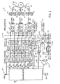
- Fig. 1 is a schematic diagram of a first exemplary embodiment of a drive circuit coupled to a motor
- Fig. 2 is a schematic diagram of a second exemplary embodiment of a drive circuit coupled to a motor
- Fig. 3 is a schematic diagram of a third exemplary embodiment of a drive circuit coupled to a motor.
- the drive circuit 10 includes a high power drive section 30 and a low power logic section 40.
- the high power drive section 30 also can be termed a power structure, while the low power logic section 40 can be termed a control structure.
- first, second and third phases of power 32, 34 and 36 are delivered to the motor 20 from six power transistor devices 41-46.
- each of the power transistor devices 41-46 is an insulated gate bipolar transistor (IGBT) although, in alternate embodiments, other types of power transistor devices (or other, non-transistor power delivery devices) can be used.
- IGBT insulated gate bipolar transistor
- Each of the first, second and third phases 32, 34 and 36 receives voltage from a respective pair of the power transistor devices 41-42, 43-44, and 45-46, respectively. Current flows toward or away from the motor 20 in each phase 32, 34, 36 depending upon which of the pair of corresponding power transistor devices is switched on.
- First, second and third coils 50, 52 and 54 are coupled in series between the motor 20 and each of the respective pairs of power transistor devices 41-42, 43-44 and 45-46.
- first, second and third coils 50, 52 and 54 the respective currents in each of the respective first, second and third phases 32, 34 and 36 can be sensed using conventional current sensing componentry (not shown).
- Each of the power transistor devices 41-46 is electrically isolated from the remainder of the high power drive section 30 and the low power logic section 40. However, the switching on and off of the power transistor devices 41-46 is nevertheless governed by signals coming from the remainder of the high power drive section 30. As shown, the power transistor devices 41-46 are light sensitive devices that respond to light signals given off by six optocoupler photodiodes 61-66, respectively. The six photodiodes 61-66 are turned on and off based upon six control signals provided from the low power logic section 40, which are respectively provided by six control line outputs 71-76 of the low power logic section 40.
- the six photodiodes 61-66 are themselves grouped into three pairs of photodiodes 61-62, 63-64 and 65-66.
- the photodiodes of each of the pairs are coupled in parallel with one another in opposite orientations, and the nodes linking the two photodiodes of each pair are then coupled to respective ones of the control line outputs 71-76 by way of respective resistors 70.
- the resistors 70 and photodiodes 61-66 are low power devices; they are considered to be part of the high power drive section insofar as they are in direct communication with the high power transistor devices 41-46, and insofar as in practice the photodiodes are typically (though not necessarily) mounted on the same circuit board as the power transistor devices rather than on a separate circuit board supporting the low power logic section.
- the respective photodiodes 61-66 are devices that are physically separate from the respective power transistor devices 41-46 or, alternately, the respective photodiodes are packaged along with their corresponding power transistor devices 41-46 in an integrated manner.
- the low power logic section 40 includes a microprocessor 80 that is coupled to a hex inverter with open collector output 90, which in turn is connected to an octal tri-state buffer/line driver 100.
- the driver 100 outputs the control signals on the control line outputs 71-76 in response to six inverter signals provided by the hex inverter 90 on six inverter signal lines 91-96.
- the six inverter signals on lines 91-96 are provided by the inverter 90 in response to six microprocessor signals output by the microprocessor 80 on six microprocessor signal lines 81-86.
- Each of the microprocessor signal lines 81-86 is coupled not only to a respective input terminal on the hex inverter 90 but also is coupled to a power supply 99 by way of a respective pull-up resistor 98.
- the power supply 99 is also coupled to the microprocessor 80 to provide power thereto.
- the power supply for the low power logic section 40 is a positive 5 volt DC power supply
- each of the pull-up resistors 98 is a 10 k ⁇ resistor.
- the hex inverter 90 essentially consists of six inverter components 97, each of which inverts a respective one of the microprocessor signals provided by way of lines 81-86 to produce the inverter signals provided on lines 91-96, respectively.
- the driver 100 merely acts as a buffer between the inverter signal lines 91-96 and the control line outputs 71-76. That is, the signal level of each respective control line output 71-76 is the same as the signal level of the corresponding inverter signal line 91-96.
- the buffering performed by the driver 100 is provided by way of six buffer components 102 within the line driver 100, each of which is coupled respectively between a respective one of the control line outputs 71-76 and its corresponding inverter signal line 91-96.
- the inverter 90 merely inverts the signals output by the microprocessor 80 along lines 81-86, the signals output by the driver 100 on the control line outputs 71-76 during normal operation have values that are opposite/inverted relative to the values of the signals on the lines 81-86.
- the driver 100 does not, however, output signals on lines 71-76 that are the same as those on lines 91-96 and inverted relative to those on lines 81-86 in all circumstances. Rather, the driver 100 only outputs the correct signals on lines 71-76 in response to the inverter signals on lines 91-96 if three conditions are met.
- power must be provided to the driver 100.
- each of the lines 91-96 is coupled to a respective pull-up resistor 104, and each of these pull-up resistors must in turn be provided with power.
- the power supply to which the resistors 104 are coupled can again be a positive 5 volt DC power supply, and each of the pull-up resistors 104 can have a value of 4.7 k ⁇ .
- the driver 100 ceases to consistently provide signals on lines 71-76 that are the same as the signals on lines 91-96 and inverted relative to the signals on lines 81-86, and instead the signals output by the driver each take on a zero value or effectively-zero value in which no current is conducted to any of the photodiodes 61-66.
- control line outputs 71-76 being nonconductive for the following reasons. If the power supply is decoupled from the pull-up resistors 104, then currents will not flow through those resistors 104 when the inverter signal lines 91-96 take on a zero value. Further, because the inverter 90 is an open collector output device, the absence of power being supplied to the pull-up resistors 104 causes the six inverter components 97 of the inverter to enter high impedance, indeterminate states.
- the inverter components 97 are in these indeterminate states, they are unable to take on high voltage values, and consequently, the lines 91-96 and input terminals of the buffer components 102 of the driver 100 remain at zero volts. Likewise, if the power supply 99 is entirely decoupled from the driver 100 itself, the buffer components 102 are unable to output nonzero currents on the control output lines 71-76. Further, if a zero voltage level is applied to the enable input 106 of the driver 100, then each of the buffer components 102 likewise is unable to provide a nonzero current on any of the control output lines 71-76.
- a first mechanism for shutting down the low power logic section 40 involves a safety relay circuit 110 that governs whether the power supply 99 is coupled to each of the pull-up resistors 104 as well as to the driver 100 itself.
- the safety relay circuit 110 includes a safety on input 112 that includes a coil 114.
- a normally-open contact 116 within the safety relay circuit 110 is closed and a second, normally-closed contact 118 within the safety relay circuit is opened.
- the closing of the normally-open contact 116 links first and second ports 120, 122 of the safety relay circuit 110 so that the power supply 99, which is coupled to the first port 120, is in turn coupled to the pull-up resistors 104 and the driver 100 itself, each of which are coupled to the second port 122.
- the present embodiment is further designed to allow for the detection of faults in the safety relay circuit 110.
- a safety on monitor can also be coupled to third and fourth ports 124, 126 of the safety relay circuit 110, between which is coupled the normally-closed contact 118.
- the safety relay circuit 110 is configured such that the normally-open contact 116 and normally-closed contact 118 are physically coupled so that only one or the other of the contacts can be closed at any given time.
- the normally-closed contact 118 remains open and thus the safety on monitor can determine that a fault has occurred due to the open-circuiting of the third and fourth ports 124, 126 and the information that the voltage has been disconnected from the coil 114. Conversely, if the normally-closed contact 118 becomes welded, then the normally-open contact 116 cannot close despite the providing of voltage across the coil 114, and consequently the driver 100 cannot provide nonzero signals on the control line outputs 71-76.
- the embodiment of Fig. 1 also includes additional logic circuitry 130 that determines whether the enable input 106 of the driver 100 is asserted.
- the additional logic circuitry 130 includes a hardware switch 132 that is coupled between ground 134 (which is also coupled to appropriate grounding terminals on the microprocessor 80, the inverter 90 and the driver 100) and a low-true input 136 of a NOR gate 138.
- a second low-true input 140 of the NOR gate 138 is coupled to the microprocessor 80 by way of a control line 142, such that the microprocessor can also provide an input to the NOR gate.
- the output of the NOR gate 138 is coupled to a buffer component 144, which in turn is coupled to the enable input 106 and also to a further pull-up resistor 146.
- the further pull-up resistor 146 is coupled to the power supply 99 by way of the same line as the other pull-up resistors 104, such that power is only supplied when the normally-open contact 116 of the safety relay circuit 110 is closed.
- the buffer 144 acts as an open collector output such that a positive, non-zero output can only be applied to the enable input 106 of the driver 100 if power is supplied to the pull-up resistor 146, that is, only if the normally-open contact 116 of the safety relay circuit 110 is closed.
- the enable input 106 only receives a positive, non-zero value such that the driver 100 is capable of outputting non-zero output signals on the control line outputs 71-76 if the normally-open contact 116 of the safety relay circuit 110 is closed and at least one of the hardware switch 132 is closed or the microprocessor 80 provides a zero-level control signal via the control line 142 to the inverter 140.
- the drive circuit 10 When implemented as shown in FIG. 1, the drive circuit 10 provides multiple, redundant avenues by which an operator or other control entity can cause the drive circuit to provide zero-level control signals via the control line outputs 71-76 to the photodiodes 61-66 such that the motor 20 ceases to receive power from the power transistor devices 41-46. While it is possible that a human operator may trigger one or both of the hardware switch 132 or the safety on input 112 of the safety relay circuit 110, the present embodiment also envisions the coupling of these inputs to other components such as an additional safety relay circuit that would be capable of providing a command to each of these inputs (such a safety relay circuit could, for example, be present in a factory environment). That is, the present embodiment is intended to be capable of being implemented in conjunction with a variety of other devices in a manner allowing those other devices to control whether the drive circuit 10 is disabled.
- the circuitry of the drive circuit 10 also is sufficiently redundant that it satisfies requirements of Category 3 of the EN 954-1 standard, which requires that no single fault in any part of the drive circuit 10 would lead to a loss of the ability to cease providing control signals such that the motor 20 might develop sustained torque.
- a failure of one of the contacts of the safety relay circuit 110 can be detected by way of the safety on monitor.
- a failure of the signals on control line outputs 71-76 to become null in response to such activation/command can be sensed by way of the coils 50, 52 and 54.
- the switch 132 is open, or the microprocessor 80 is providing a zero-level signal on the control line 142, then none of the coils 50, 52, 54 should experience any current and, if current is sensed, a warning signal is generated.
- the sensed current information obtained by way of the coils 50, 52 and 54 is provided to and used by the microprocessor 80.
- the drive circuit 10 satisfies Category 3 of the EN 954-1 standard is not meant to indicate that the drive circuit 10 guarantees that electrical voltage is not provided to the motor 20. Indeed, despite the nullification of the control line outputs 71-76, it is still conceivable that one or more of the power transistor devices 41-46 would apply voltage to the motor 20.
- the motor 20 can only develop sustained rotation and torque if the power transistor devices 41-46 apply voltage at specific times in a pulse width modulated (PWM) manner determined by the microprocessor 80, inadvertent conduction of currents by any of the power transistor devices 41-46 would only, at most, cause the motor to experience a one-time movement of a limited number of degrees, such as 180 degrees for a two-pole motor or 90 degrees for a four-pole motor. If the motor 20 is running when either the safety on input 112 is triggered or the enable input 106 receives a low level signal due to the triggering of the switch 132 or a signal from the microprocessor 80, the motor 20 will coast to a standstill.
- PWM pulse width modulated
- the safety relay circuit input to the driver 100 prevents power from being provided to the control line outputs 71-76, while the actuation of the enable input 106 of the driver 100, as actuated by the switch 132 or the microprocessor 80 by way of the control line 142, acts as a logic inhibit of the control line outputs.
- FIG. 2 an alternate embodiment of a drive circuit 210 that somewhat differs from the drive circuit 10 of FIG. 1 is shown coupled to the motor 20.
- the drive circuit 210 does include the same high power drive section 30 as the drive circuit 10, and a low power logic section 240 of the drive circuit includes the same microprocessor 80, inverter 90, pull-up resistors 98, 104 and 146, and additional logic circuitry 130 as the low power logic section 40.
- the additional logic circuitry 130 provides signals to an enable input 106 of an octal tri-state buffer/line driver 200 of the logic circuit 240.
- the logic circuit 240 differs from the logic circuit 40 in that the driver 200 of the logic circuit 240 is not coupled to the power supply 99 by way of any safety relay.
- a safety relay circuit 310 that is employed in the low power logic section 240 is essentially an inverted version of the safety relay circuit 110.
- the safety relay circuit 310 includes first and second ports 320 and 322 that are respectively coupled to the ground 134 and to the pull-up resistors 104 and 146, with a normally-closed contact 316 coupled between those ports.
- third and fourth ports 324 and 326 of the safety relay circuit 310 have a normally-open contact 318 coupled between them.
- the power supply 99 is coupled to the pull-up resistors 104 and 146 and to the second port 322 by a low-level resistance (in this example, a 330 ohm resistor).
- the normally-closed contact 316 is opened such that the power supply 99 is effectively connected to the pull-up resistors 104, 146, thereby allowing the driver 200 to receive non-zero signals from the inverter 90.
- the pull-up resistors 104 and 146 are coupled to ground, thereby preventing the driver 200 from outputting non-zero signals on the control line outputs 71-76.
- the normally-closed contact 316 and normally-open contact 318 of the safety relay circuit 310 are physically coupled such that only one of the contacts can be closed at any given time, such that a welding of either of the normally-closed and normally-opened contacts can be detected.
- the drive circuit 210 of FIG. 2 is somewhat simpler to implement and for that reason is somewhat preferred for that reason, albeit the embodiment of FIG. 1 satisfies certain standards that may not be satisfied by the circuit of FIG. 2.
- a third embodiment of the present invention shows a drive circuit 410 having components identical to the drive circuit 110 except insofar as the safety relay circuit 110 has been replaced with a circuit 400 that includes a DC-to-DC conversion circuit 420.
- another device such as another safety relay circuit provided by a third party would be coupled to input terminal 412 of the circuit 400.
- the circuit would then convert power signals provided by that other device into an output signal 415 that would govern the voltage applied to the pull-up resistors 104, 146 and the power supplied to the driver 100.
- the input signals at the input terminal 412 would be isolated from the output signal 415, and the input signals could differ in their voltage range from that required by the driver 100 in an arbitrary manner (in the embodiment shown, for example, the input signals 412 can range from 0 to 12 Volts signals, while the output signal 415 can range from 0 to 5 Volts).
- the embodiment of FIG. 3 shows a DC-to-DC conversion circuit that provides electrical isolation, in alternate embodiments, opto-isolators or other devices could be employed to provide isolation.
- a DC-to-DC conversion device is advantageous insofar as it provides a reliable shut-down mechanism since it cannot operate without power being applied.
- the present invention is not intended to be limited to these particular electrical circuits. Rather, the present invention is intended to encompass a variety of electrical and other control circuits in which the delivery of high power levels to a high power device is governed in part by low power circuitry, and in which there are one or more control mechanisms for disabling the low power circuitry to effectively stop the operation of the high power device without taking any action to disable or disconnect the high power drive circuit devices that are directly coupled to that high power load. Indeed, the present invention is intended to encompass any such dual-stage drive circuits in which disablement occurs via the low power stage, regardless of the type of high power load that those drive circuits are powering.
- the present invention is intended to encompass control/drive circuits that are formed from multiple distinct modules.
- all of the components of the drive circuit 210 need not be included on a single circuit board. Rather, in some embodiments, all of the low power logic circuit 240 of the drive circuit 210 of FIG. 2 would be included within a primary module except for the safety relay circuit 310, which could be implemented on an auxiliary module. In such an embodiment, the drive circuit 210 could be operated to control the high power drive circuit 30 and the motor 20 as normal without the auxiliary module.
- auxiliary module including a safety relay circuit or other circuit such as circuits 110,310 and 400 could be implemented in a variety of manners, such as on a plug-in-module or as part of an external cable.
- the present invention is intended to encompass embodiments in which a main control device can be coupled to one or more other devices, which depending upon the embodiment might be required or optional (or even after-market) devices.
- safety in an industrial or other process depends on a wide variety of factors outside of the scope of the present invention including, for example: design of the safety system; installation and maintenance of the components of the safety system; the cooperation and training of individuals using the safety system; and consideration of the failure modes of the other components being utilized.
- design of the safety system including, for example: design of the safety system; installation and maintenance of the components of the safety system; the cooperation and training of individuals using the safety system; and consideration of the failure modes of the other components being utilized.
- the present invention is intended to be highly reliable, all physical systems are susceptible to failure and provision must be made for such failure.
- the above description has been that of a preferred embodiment of the present invention. It will occur to those that practice the art that many modifications may be made without departing from the spirit and scope of the invention. In order to apprise the public of the various embodiments that may fall within the scope of the invention, the following claims are made.
- the drive circuit includes a high power circuit capable of being coupled to the load and delivering the high level power thereto, and a low power circuit that controls the high power circuit.
- the low power circuit includes a first circuit portion that provides at least one control signal that is at least indirectly communicated to the high power circuit and that controls the delivering of the high level power by the high power circuit, and a second circuit portions coupled to the first circuit portion.
- the second circuit portion is capable of disabling the first circuit portion so that the at least one control signal avoids taking on values that would result in the high power circuit delivering the high level power to the load.
Landscapes
- Engineering & Computer Science (AREA)
- Power Engineering (AREA)
- Inverter Devices (AREA)
- Control Of Electric Motors In General (AREA)
- Direct Current Feeding And Distribution (AREA)
Applications Claiming Priority (2)
| Application Number | Priority Date | Filing Date | Title |
|---|---|---|---|
| US730430 | 2000-12-05 | ||
| US10/730,430 US8593768B2 (en) | 2003-12-08 | 2003-12-08 | Apparatus and method for disabling the operation of high power devices |
Publications (3)
| Publication Number | Publication Date |
|---|---|
| EP1542330A2 true EP1542330A2 (de) | 2005-06-15 |
| EP1542330A3 EP1542330A3 (de) | 2008-03-12 |
| EP1542330B1 EP1542330B1 (de) | 2013-02-20 |
Family
ID=34523012
Family Applications (1)
| Application Number | Title | Priority Date | Filing Date |
|---|---|---|---|
| EP04029071A Expired - Lifetime EP1542330B1 (de) | 2003-12-08 | 2004-12-08 | Mittel und Verfahren zur Verhinderung des Betreibs von Hochleistungsvorrichtungen |
Country Status (2)
| Country | Link |
|---|---|
| US (2) | US8593768B2 (de) |
| EP (1) | EP1542330B1 (de) |
Cited By (3)
| Publication number | Priority date | Publication date | Assignee | Title |
|---|---|---|---|---|
| EP2405568A1 (de) * | 2010-07-05 | 2012-01-11 | Gefran S.p.A. | Elektronische Energievorrichtung zur Steuerung der Bewegung von Wechselstrom-Elektromotoren, die auf sichere Weise angehalten werden |
| CN106849826A (zh) * | 2017-03-06 | 2017-06-13 | 四川大能科技有限公司 | 一种内置大电流继电器的电动车电机驱动器 |
| EP3048721B1 (de) | 2014-11-21 | 2021-06-30 | B&R Industrial Automation GmbH | Vorrichtung und ein verfahren zur sicheren ansteuerung eines halbleiterschalters eines wechselrichters |
Families Citing this family (7)
| Publication number | Priority date | Publication date | Assignee | Title |
|---|---|---|---|---|
| US7253577B2 (en) * | 2005-05-20 | 2007-08-07 | Rockwell Automation Technologies, Inc. | Independent safety processor for disabling the operation of high power devices |
| JP5412993B2 (ja) * | 2009-06-26 | 2014-02-12 | 富士電機株式会社 | 安全装置および電力変換器 |
| US20110034920A1 (en) * | 2009-08-07 | 2011-02-10 | Naing Htwe W | Variable dual mode tissue heating system controller |
| US8638539B2 (en) | 2011-07-27 | 2014-01-28 | The Watt Stopper, Inc. | Method and apparatus for isolating high voltage power control elements |
| JP5552564B1 (ja) | 2013-09-24 | 2014-07-16 | 川崎重工業株式会社 | 多軸ロボットの動力遮断装置及び多軸ロボット |
| DE102015120023A1 (de) * | 2015-11-19 | 2017-05-24 | Keba Ag | Elektrischer Antrieb für einen industriellen Roboter |
| US11909199B2 (en) | 2021-02-02 | 2024-02-20 | Rockwell Automation Technologies, Inc. | Functional safety techniques for industrial automation devices |
Citations (1)
| Publication number | Priority date | Publication date | Assignee | Title |
|---|---|---|---|---|
| DE20117222U1 (de) | 2001-10-24 | 2002-01-17 | Siemens AG, 80333 München | Produktionsmaschine mit einem Antriebsverband bestehend aus Antriebssektionen |
Family Cites Families (21)
| Publication number | Priority date | Publication date | Assignee | Title |
|---|---|---|---|---|
| US4247189A (en) * | 1978-09-22 | 1981-01-27 | Canon Kabushiki Kaisha | Camera with built-in electric wind-up mechanism |
| US4637547A (en) * | 1982-08-05 | 1987-01-20 | Hiniker Company | Control method and apparatus for liquid distributor |
| US4630210A (en) * | 1984-10-04 | 1986-12-16 | Pitney Bowes Inc. | Microprocessor controlled d.c. motor for controlling a load |
| DE4136514C2 (de) * | 1991-11-06 | 1994-08-18 | Heraeus Sepatech | Schaltungsanordnung zur Drehzahlsteuerung eines als Zentrifugenantrieb dienenden dreiphasigen Induktionsmotors |
| US5524556A (en) * | 1995-06-09 | 1996-06-11 | Texas Instruments Incorporated | Induced draft fan control for use with gas furnaces |
| US5828200A (en) * | 1995-11-21 | 1998-10-27 | Phase Iii | Motor control system for variable speed induction motors |
| US5764024A (en) * | 1997-04-07 | 1998-06-09 | Motorola, Inc. | Pulse width modulator (PWM) system with low cost dead time distortion correction |
| US5904666A (en) * | 1997-08-18 | 1999-05-18 | L.Vad Technology, Inc. | Method and apparatus for measuring flow rate and controlling delivered volume of fluid through a valve aperture |
| JPH11136801A (ja) * | 1997-10-24 | 1999-05-21 | Denso Corp | 複数バッテリ型電気自動車用駆動装置 |
| DE19816046A1 (de) | 1998-04-09 | 1999-10-28 | Bosch Gmbh Robert | Sicherheitsvorrichtung für einen Antrieb |
| ES2158782B1 (es) * | 1998-05-12 | 2002-03-01 | Mannesmann Sachs Ag | Sistema y procedimiento de mando para un motor electrico excitado permanentemente con al menos una fase. |
| JP2001282301A (ja) | 2000-04-03 | 2001-10-12 | Matsushita Electric Ind Co Ltd | ロボットの制御装置 |
| DE10059172A1 (de) | 2000-11-29 | 2002-06-13 | Siemens Ag | Sichere Geschwindigkeitsüberwachung für geberlose Drehstromantriebe |
| DE10059173C5 (de) * | 2000-11-29 | 2004-07-15 | Siemens Ag | Antriebssteuerung für einen Drehstrommotor über einen Wechselrichter in sicherer Technik |
| DE10207834A1 (de) | 2001-02-27 | 2002-09-05 | Sew Eurodrive Gmbh & Co | Anlage und Verfahren |
| DE10206107B4 (de) | 2001-02-27 | 2020-08-13 | Sew-Eurodrive Gmbh & Co Kg | Umrichter und Verwendung |
| EP1253490B1 (de) | 2001-04-25 | 2011-08-17 | Siemens Aktiengesellschaft | Verfahren und Vorrichtung zur sicheren Geschwindigkeitsüberwachung |
| US6573672B2 (en) | 2001-06-29 | 2003-06-03 | Honeywell International Inc. | Fail passive servo controller |
| JP3632657B2 (ja) * | 2001-12-20 | 2005-03-23 | トヨタ自動車株式会社 | 電圧変換装置 |
| DE10261452B4 (de) | 2002-12-31 | 2011-02-03 | Danfoss Drives A/S | Motorsteuerung mit einer Steuereinrichtung und einer Sicherheitsvorrichtung zum sicheren Abschalten eines Motors |
| DE10261454B4 (de) | 2002-12-31 | 2010-04-08 | Danfoss Drives A/S | Motorsteuerung mit sicherem Halt |
-
2003
- 2003-12-08 US US10/730,430 patent/US8593768B2/en active Active
-
2004
- 2004-12-08 EP EP04029071A patent/EP1542330B1/de not_active Expired - Lifetime
-
2013
- 2013-09-20 US US14/032,960 patent/US8848324B2/en not_active Expired - Lifetime
Patent Citations (1)
| Publication number | Priority date | Publication date | Assignee | Title |
|---|---|---|---|---|
| DE20117222U1 (de) | 2001-10-24 | 2002-01-17 | Siemens AG, 80333 München | Produktionsmaschine mit einem Antriebsverband bestehend aus Antriebssektionen |
Non-Patent Citations (1)
| Title |
|---|
| HORDEN I. ET AL.: "Machine Design", vol. 60, 21 July 1988, PENTON MEDIA, article "Processors that simplify motor control", pages: 85 - 88 |
Cited By (5)
| Publication number | Priority date | Publication date | Assignee | Title |
|---|---|---|---|---|
| EP2405568A1 (de) * | 2010-07-05 | 2012-01-11 | Gefran S.p.A. | Elektronische Energievorrichtung zur Steuerung der Bewegung von Wechselstrom-Elektromotoren, die auf sichere Weise angehalten werden |
| EP3048721B1 (de) | 2014-11-21 | 2021-06-30 | B&R Industrial Automation GmbH | Vorrichtung und ein verfahren zur sicheren ansteuerung eines halbleiterschalters eines wechselrichters |
| EP3048721B2 (de) † | 2014-11-21 | 2025-06-04 | B&R Industrial Automation GmbH | Vorrichtung und ein verfahren zur sicheren ansteuerung eines halbleiterschalters eines wechselrichters |
| CN106849826A (zh) * | 2017-03-06 | 2017-06-13 | 四川大能科技有限公司 | 一种内置大电流继电器的电动车电机驱动器 |
| CN106849826B (zh) * | 2017-03-06 | 2018-03-09 | 四川大能科技有限公司 | 一种内置大电流继电器的电动车电机驱动器 |
Also Published As
| Publication number | Publication date |
|---|---|
| US20140021896A1 (en) | 2014-01-23 |
| EP1542330A3 (de) | 2008-03-12 |
| US8593768B2 (en) | 2013-11-26 |
| EP1542330B1 (de) | 2013-02-20 |
| US8848324B2 (en) | 2014-09-30 |
| US20050122641A1 (en) | 2005-06-09 |
Similar Documents
| Publication | Publication Date | Title |
|---|---|---|
| US8848324B2 (en) | Apparatus and method for disabling the operation of high power devices | |
| EP1724915B1 (de) | Unabhängiger sicherheitsprozessor zum abschalten von leistungsgeräten | |
| US7586725B2 (en) | Method of providing a secondary means of overload protection and leakage current protection in applications using solid state power controllers | |
| US9293285B2 (en) | Safety circuit arrangement for connection or failsafe disconnection of a hazardous installation | |
| EP2592502B1 (de) | Sicherheitssteuerungssystem | |
| CN111465777B (zh) | 刹车驱动控制电路及其故障检测方法 | |
| US11777436B2 (en) | Method and system for a safety concept for an AC battery | |
| US7952314B2 (en) | Electronic control device of an electrical drive system with redundant disconnection device | |
| US6204751B1 (en) | Current inrush limiting circuit with fast reset | |
| EP2405568B1 (de) | Elektronische Energievorrichtung zur Steuerung der Bewegung von Wechselstrom-Elektromotoren, die auf sichere Weise angehalten werden | |
| EP1952500B1 (de) | Einrichtung zur begrenzung des stroms eines elektrischen geräts | |
| EP3786735B1 (de) | Strombegrenzungsschaltung und - verfahren für ausgangs-module | |
| EP3972124B1 (de) | Eingebettete elektronische motorabschaltung und verfahren | |
| KR200315061Y1 (ko) | 3상 교류 전원의 돌입 전류 방지 장치 | |
| KR100686027B1 (ko) | 전기기기의 전류 제한 안전회로 | |
| JP7281699B2 (ja) | ブレーキ駆動制御回路とその故障検出方法 | |
| CN101361245B (zh) | 电器限流装置 | |
| CN113746381B (zh) | 一种电机的制动控制装置、方法和电机 | |
| JP2023058754A (ja) | モータ駆動装置 | |
| JP2019213444A (ja) | インバータ保護装置 | |
| JPH09172782A (ja) | インバータの主回路保護装置 | |
| KR100425110B1 (ko) | 인버터 세탁기의 클러치 제어장치 및 방법 | |
| JP2023165647A (ja) | 特に電気的及び/又は電子的負荷の監視されたスイッチオンのための安全スイッチングデバイス | |
| US7696647B2 (en) | Coupling node | |
| KR20010077755A (ko) | 배전 자동화 시스템 |
Legal Events
| Date | Code | Title | Description |
|---|---|---|---|
| PUAI | Public reference made under article 153(3) epc to a published international application that has entered the european phase |
Free format text: ORIGINAL CODE: 0009012 |
|
| AK | Designated contracting states |
Kind code of ref document: A2 Designated state(s): AT BE BG CH CY CZ DE DK EE ES FI FR GB GR HU IE IS IT LI LT LU MC NL PL PT RO SE SI SK TR |
|
| AX | Request for extension of the european patent |
Extension state: AL BA HR LV MK YU |
|
| PUAL | Search report despatched |
Free format text: ORIGINAL CODE: 0009013 |
|
| AK | Designated contracting states |
Kind code of ref document: A3 Designated state(s): AT BE BG CH CY CZ DE DK EE ES FI FR GB GR HU IE IS IT LI LT LU MC NL PL PT RO SE SI SK TR |
|
| AX | Request for extension of the european patent |
Extension state: AL BA HR LV MK YU |
|
| 17P | Request for examination filed |
Effective date: 20080627 |
|
| AKX | Designation fees paid |
Designated state(s): DE FR GB IT |
|
| 17Q | First examination report despatched |
Effective date: 20090210 |
|
| REG | Reference to a national code |
Ref country code: DE Ref legal event code: R079 Ref document number: 602004041049 Country of ref document: DE Free format text: PREVIOUS MAIN CLASS: H02H0007122000 Ipc: H02M0001092000 |
|
| GRAP | Despatch of communication of intention to grant a patent |
Free format text: ORIGINAL CODE: EPIDOSNIGR1 |
|
| RIC1 | Information provided on ipc code assigned before grant |
Ipc: H02P 29/02 20060101ALI20120808BHEP Ipc: H02M 1/092 20060101AFI20120808BHEP Ipc: H02M 7/5387 20070101ALI20120808BHEP Ipc: H02M 1/32 20070101ALI20120808BHEP |
|
| GRAS | Grant fee paid |
Free format text: ORIGINAL CODE: EPIDOSNIGR3 |
|
| GRAA | (expected) grant |
Free format text: ORIGINAL CODE: 0009210 |
|
| AK | Designated contracting states |
Kind code of ref document: B1 Designated state(s): DE FR GB IT |
|
| REG | Reference to a national code |
Ref country code: GB Ref legal event code: FG4D |
|
| REG | Reference to a national code |
Ref country code: DE Ref legal event code: R096 Ref document number: 602004041049 Country of ref document: DE Effective date: 20130418 |
|
| PLBE | No opposition filed within time limit |
Free format text: ORIGINAL CODE: 0009261 |
|
| STAA | Information on the status of an ep patent application or granted ep patent |
Free format text: STATUS: NO OPPOSITION FILED WITHIN TIME LIMIT |
|
| PG25 | Lapsed in a contracting state [announced via postgrant information from national office to epo] |
Ref country code: IT Free format text: LAPSE BECAUSE OF FAILURE TO SUBMIT A TRANSLATION OF THE DESCRIPTION OR TO PAY THE FEE WITHIN THE PRESCRIBED TIME-LIMIT Effective date: 20130220 |
|
| 26N | No opposition filed |
Effective date: 20131121 |
|
| REG | Reference to a national code |
Ref country code: DE Ref legal event code: R097 Ref document number: 602004041049 Country of ref document: DE Effective date: 20131121 |
|
| PGFP | Annual fee paid to national office [announced via postgrant information from national office to epo] |
Ref country code: GB Payment date: 20141229 Year of fee payment: 11 |
|
| PGFP | Annual fee paid to national office [announced via postgrant information from national office to epo] |
Ref country code: FR Payment date: 20141217 Year of fee payment: 11 |
|
| PGFP | Annual fee paid to national office [announced via postgrant information from national office to epo] |
Ref country code: DE Payment date: 20141230 Year of fee payment: 11 |
|
| REG | Reference to a national code |
Ref country code: DE Ref legal event code: R119 Ref document number: 602004041049 Country of ref document: DE |
|
| GBPC | Gb: european patent ceased through non-payment of renewal fee |
Effective date: 20151208 |
|
| REG | Reference to a national code |
Ref country code: FR Ref legal event code: ST Effective date: 20160831 |
|
| PG25 | Lapsed in a contracting state [announced via postgrant information from national office to epo] |
Ref country code: DE Free format text: LAPSE BECAUSE OF NON-PAYMENT OF DUE FEES Effective date: 20160701 Ref country code: GB Free format text: LAPSE BECAUSE OF NON-PAYMENT OF DUE FEES Effective date: 20151208 |
|
| PG25 | Lapsed in a contracting state [announced via postgrant information from national office to epo] |
Ref country code: FR Free format text: LAPSE BECAUSE OF NON-PAYMENT OF DUE FEES Effective date: 20151231 |