EP1542288A1 - Method for manufacturing compound semiconductor wafer and compound semiconductor device - Google Patents
Method for manufacturing compound semiconductor wafer and compound semiconductor device Download PDFInfo
- Publication number
- EP1542288A1 EP1542288A1 EP03784504A EP03784504A EP1542288A1 EP 1542288 A1 EP1542288 A1 EP 1542288A1 EP 03784504 A EP03784504 A EP 03784504A EP 03784504 A EP03784504 A EP 03784504A EP 1542288 A1 EP1542288 A1 EP 1542288A1
- Authority
- EP
- European Patent Office
- Prior art keywords
- layer
- compound semiconductor
- base layer
- growth
- base
- Prior art date
- Legal status (The legal status is an assumption and is not a legal conclusion. Google has not performed a legal analysis and makes no representation as to the accuracy of the status listed.)
- Withdrawn
Links
Images




Classifications
-
- H—ELECTRICITY
- H10—SEMICONDUCTOR DEVICES; ELECTRIC SOLID-STATE DEVICES NOT OTHERWISE PROVIDED FOR
- H10D—INORGANIC ELECTRIC SEMICONDUCTOR DEVICES
- H10D10/00—Bipolar junction transistors [BJT]
- H10D10/80—Heterojunction BJTs
- H10D10/821—Vertical heterojunction BJTs
-
- H—ELECTRICITY
- H10—SEMICONDUCTOR DEVICES; ELECTRIC SOLID-STATE DEVICES NOT OTHERWISE PROVIDED FOR
- H10D—INORGANIC ELECTRIC SEMICONDUCTOR DEVICES
- H10D10/00—Bipolar junction transistors [BJT]
- H10D10/01—Manufacture or treatment
- H10D10/021—Manufacture or treatment of heterojunction BJTs [HBT]
-
- H—ELECTRICITY
- H10—SEMICONDUCTOR DEVICES; ELECTRIC SOLID-STATE DEVICES NOT OTHERWISE PROVIDED FOR
- H10D—INORGANIC ELECTRIC SEMICONDUCTOR DEVICES
- H10D62/00—Semiconductor bodies, or regions thereof, of devices having potential barriers
- H10D62/80—Semiconductor bodies, or regions thereof, of devices having potential barriers characterised by the materials
- H10D62/85—Semiconductor bodies, or regions thereof, of devices having potential barriers characterised by the materials being Group III-V materials, e.g. GaAs
- H10D62/854—Semiconductor bodies, or regions thereof, of devices having potential barriers characterised by the materials being Group III-V materials, e.g. GaAs further characterised by the dopants
-
- H—ELECTRICITY
- H10—SEMICONDUCTOR DEVICES; ELECTRIC SOLID-STATE DEVICES NOT OTHERWISE PROVIDED FOR
- H10P—GENERIC PROCESSES OR APPARATUS FOR THE MANUFACTURE OR TREATMENT OF DEVICES COVERED BY CLASS H10
- H10P14/00—Formation of materials, e.g. in the shape of layers or pillars
- H10P14/20—Formation of materials, e.g. in the shape of layers or pillars of semiconductor materials
- H10P14/24—Formation of materials, e.g. in the shape of layers or pillars of semiconductor materials using chemical vapour deposition [CVD]
-
- H—ELECTRICITY
- H10—SEMICONDUCTOR DEVICES; ELECTRIC SOLID-STATE DEVICES NOT OTHERWISE PROVIDED FOR
- H10P—GENERIC PROCESSES OR APPARATUS FOR THE MANUFACTURE OR TREATMENT OF DEVICES COVERED BY CLASS H10
- H10P14/00—Formation of materials, e.g. in the shape of layers or pillars
- H10P14/20—Formation of materials, e.g. in the shape of layers or pillars of semiconductor materials
- H10P14/29—Formation of materials, e.g. in the shape of layers or pillars of semiconductor materials characterised by the substrates
- H10P14/2901—Materials
- H10P14/2907—Materials being Group IIIA-VA materials
- H10P14/2911—Arsenides
-
- H—ELECTRICITY
- H10—SEMICONDUCTOR DEVICES; ELECTRIC SOLID-STATE DEVICES NOT OTHERWISE PROVIDED FOR
- H10P—GENERIC PROCESSES OR APPARATUS FOR THE MANUFACTURE OR TREATMENT OF DEVICES COVERED BY CLASS H10
- H10P14/00—Formation of materials, e.g. in the shape of layers or pillars
- H10P14/20—Formation of materials, e.g. in the shape of layers or pillars of semiconductor materials
- H10P14/32—Formation of materials, e.g. in the shape of layers or pillars of semiconductor materials characterised by intermediate layers between substrates and deposited layers
- H10P14/3202—Materials thereof
- H10P14/3214—Materials thereof being Group IIIA-VA semiconductors
- H10P14/3221—Arsenides
-
- H—ELECTRICITY
- H10—SEMICONDUCTOR DEVICES; ELECTRIC SOLID-STATE DEVICES NOT OTHERWISE PROVIDED FOR
- H10P—GENERIC PROCESSES OR APPARATUS FOR THE MANUFACTURE OR TREATMENT OF DEVICES COVERED BY CLASS H10
- H10P14/00—Formation of materials, e.g. in the shape of layers or pillars
- H10P14/20—Formation of materials, e.g. in the shape of layers or pillars of semiconductor materials
- H10P14/34—Deposited materials, e.g. layers
- H10P14/3402—Deposited materials, e.g. layers characterised by the chemical composition
- H10P14/3414—Deposited materials, e.g. layers characterised by the chemical composition being group IIIA-VIA materials
- H10P14/3421—Arsenides
-
- H—ELECTRICITY
- H10—SEMICONDUCTOR DEVICES; ELECTRIC SOLID-STATE DEVICES NOT OTHERWISE PROVIDED FOR
- H10P—GENERIC PROCESSES OR APPARATUS FOR THE MANUFACTURE OR TREATMENT OF DEVICES COVERED BY CLASS H10
- H10P14/00—Formation of materials, e.g. in the shape of layers or pillars
- H10P14/20—Formation of materials, e.g. in the shape of layers or pillars of semiconductor materials
- H10P14/34—Deposited materials, e.g. layers
- H10P14/3438—Doping during depositing
- H10P14/3441—Conductivity type
- H10P14/3444—P-type
-
- H—ELECTRICITY
- H10—SEMICONDUCTOR DEVICES; ELECTRIC SOLID-STATE DEVICES NOT OTHERWISE PROVIDED FOR
- H10D—INORGANIC ELECTRIC SEMICONDUCTOR DEVICES
- H10D62/00—Semiconductor bodies, or regions thereof, of devices having potential barriers
- H10D62/80—Semiconductor bodies, or regions thereof, of devices having potential barriers characterised by the materials
- H10D62/82—Heterojunctions
- H10D62/824—Heterojunctions comprising only Group III-V materials heterojunctions, e.g. GaN/AlGaN heterojunctions
-
- H—ELECTRICITY
- H10—SEMICONDUCTOR DEVICES; ELECTRIC SOLID-STATE DEVICES NOT OTHERWISE PROVIDED FOR
- H10D—INORGANIC ELECTRIC SEMICONDUCTOR DEVICES
- H10D62/00—Semiconductor bodies, or regions thereof, of devices having potential barriers
- H10D62/80—Semiconductor bodies, or regions thereof, of devices having potential barriers characterised by the materials
- H10D62/85—Semiconductor bodies, or regions thereof, of devices having potential barriers characterised by the materials being Group III-V materials, e.g. GaAs
Definitions
- the present invention relates to a method for producing a compound semiconductor wafer used for production of hetero junction bi-polar transistors (HBTs), and to a compound semiconductor device.
- HBTs hetero junction bi-polar transistors
- Hetero junction bi-polar transistors are bi-polar transistors in which an emitter-base junction is a hetero junction using a material greater in band gap than a base layer for an emitter layer in order to enhance the emitter injection efficiency, and since HBT is suitable as semiconductor devices used in the frequency area higher than microwave band, they are expected to be used as semiconductor devices for portable telephones of the next generation.
- HBT The structure of HBT is as follows.
- a GaAs-based HBT generally an n + -GaAs layer (sub-collector layer), an n-GaAs layer (collector layer), a p-GaAs layer (base layer), an n-InGaP layer (emitter layer) and an n-GaAs layer (sub-emitter layer) are in turn grown as crystal on a semi-insulated GaAs substrate by a Metal Organic Chemical Vapor Deposition (MOCVD), thereby forming a thin film crystal wafer having the above-mentioned layer structure where a pn junction which is an emitter-base junction is of a structure of a hetero junction, and an HBT is produced using the resulting wafer.
- MOCVD Metal Organic Chemical Vapor Deposition
- FIG. 7 schematically shows a structure of the conventional general GaAs-based HBT.
- a sub-collector layer 102 comprising an n + -GaAs layer, a collector layer 103 comprising an n-GaAs layer, a base layer 104 comprising a p-GaAs layer, an emitter layer 105 comprising an n-InGaP layer, a sub-emitter layer 106 comprising an n + -GaAs layer and an emitter contact layer 107 comprising an n + -InGaAs layer are in this turn formed as semiconductor thin film crystal layers on a semi-insulated GaAs substrate 101 by a suitable vapor growth method such as MOCVD method, and a collector electrode 108, a base electrode 109 and an emitter electrode 110 are formed on the sub-collector layer 102, the base layer 104 and the emitter contact layer 107, respectively.
- a suitable vapor growth method such as MOCVD method
- JP-A-3-110829 proposes a method for producing a compound semiconductor thin film in which the substrate temperature during the growth of the compound semiconductor thin film is set in the range of 450-650°C and the feeding molar ratio of the raw material of Group V and that of Group III is set in the range of 0.3-2.5.
- the carrier concentration can be controlled to 1 ⁇ 10 18 cm -3 - 1 ⁇ 10 20 cm -3 , but the method has a problem that when the feeding molar ratio of the raw material of Group V and that of Group III and the growth temperature are determined, the carrier concentration is determined thereby and thus it is difficult to control the carrier concentration to a desired value.
- the object of the present invention is to provide a method for producing a compound semiconductor wafer and a compound semiconductor device which can solve the above problems in the conventional technologies.
- the object of the present invention is to provide a method for producing a compound semiconductor wafer where control of carrier concentration becomes possible by externally adding impurities, whereby a base layer of good crystallinity can be formed, and to provide a compound semiconductor device using the wafer.
- the present invention is employed under such conditions as giving a growth determined by a Group V gas flow rate-feed as the growth conditions of the base layer, and thus the crystallinity of the base layer is improved and the current gain can be remarkably improved.
- the V/III ratio in the range of 1.0-0.3, the growth of the base layer can be a growth determined by a Group V gas flow rate-feed.
- the V/III ratio here is a feed ratio of the raw material of Group V and that of Group III during the growth of Groups III-V compound semiconductor crystals.
- the raw materials are generally fed in the state of gas from gas cylinders or bubblers.
- the feed rate of gas from a gas cylinder is controlled by a flow rate controlling apparatus such as a mass flow controller located on a feeding line, and (gas concentration in cylinder) ⁇ (gas flow rate) is an actual flow rate of the raw material.
- the feed rate of gas from a bubbler is controlled by a flow rate controlling apparatus such as a mass flow controller located on a feeding line of carrier gas flowed to the bubbler, and (carrier gas flow rate) ⁇ (vapor pressure of raw material in bubbler)/(inner pressure of bubbler) is an actual flow rate of the raw material.
- a flow rate controlling apparatus such as a mass flow controller located on a feeding line of carrier gas flowed to the bubbler
- carrier gas flow rate) ⁇ (vapor pressure of raw material in bubbler)/(inner pressure of bubbler) is an actual flow rate of the raw material.
- V/III ratio The ratio of feed rate of the raw material of Group V and that of Group III on the actual flow rates of the raw materials fed by the above systems is generally called V/III ratio.
- V/III ratio is also used according to this definition.
- the first embodiment of the present invention proposes a method for producing a compound semiconductor wafer used for the production of HBT by vapor growth of a sub-collector layer, a collector layer, a base layer and an emitter layer in this turn on a compound semiconductor substrate using MOCVD method, wherein the base layer is a p-type compound semiconductor thin film layer containing at least one of Ga, Al and In as a Group III element and as a Group V element and is grown under such conditions that the growth rate gives a growth determined by a Group V gas flow rate-feed.
- crystallinity of the grown base layer is improved, the recombination current in the base layer can be decreased, and the current gain of HBT can be increased.
- the second embodiment of the present invention proposes a method for producing a compound semiconductor wafer according to the invention of claim 1, wherein the base layer is grown with the V/III ratio being in the range of 0.3-1.0.
- the third embodiment of the present invention proposes a method for producing a compound semiconductor wafer according to the invention of claim 1 or 2, wherein the adjustment of carrier concentration in the base layer is controlled by the flow rate of methane halide.
- the fourth embodiment of the present invention proposes a method for producing a compound semiconductor wafer according to the invention of claim 1 or 2, wherein the adjustment of carrier concentration in the base layer is controlled by the flow rate of CBrCl 3 .
- the fifth embodiment of the present invention proposes a compound semiconductor device comprising a sub-collector layer, a collector layer, a base layer and an emitter layer formed as thin film crystal layers in this turn on a compound semiconductor substrate by vapor growth, wherein the life time of minority carriers in the base layer is 200 psec or longer.
- the sixth embodiment of the present invention proposes a compound semiconductor device containing a hetero junction bi-polar transistor and comprising a sub-collector layer, a collector layer, a base layer and an emitter layer formed as thin film crystal layers in this turn on a compound semiconductor substrate by vapor growth, wherein the ratio of current gain/base sheet resistance of the hetero junction bi-polar transistor is 0.60 or more.
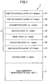
- FIG. 1 schematically shows a layer structure of one example of the thin film crystal wafer for HBT which is produced by the method of the present invention.
- This thin film crystal wafer is a compound semiconductor wafer used for producing a GaAs-based HBT, and one example of the embodiments of producing the semiconductor wafer having the layer structure shown in FIG. 1 by the method of the present invention will be explained below. Accordingly, this example should not be construed as limiting the method of the present invention to only the production of the compound semiconductor wafer having the structure as shown in FIG. 1.
- the semiconductor wafer 1 shown in FIG. 1 has the following structure.
- the semiconductor wafer 1 is constructed by in this turn laminating a plurality of semiconductor thin film crystal growth layers on a GaAs substrate 2 comprising semi-insulated GaAs compound semiconductor crystals by MOCVD method.
- the semiconductor wafer 1 will be explained referring to FIG. 1.
- the GaAs substrate 2 comprises a semi-insulated GaAs (001) layer, and a buffer layer 3 comprising an i-GaAs layer is formed on the GaAs substrate 2.
- the HBT functional layers 4 include an n + -GaAs layer acting as a sub-collector layer 41 and an n - -GaAs layer acting as a collector layer 42 which are in this turn formed as semiconductor epitaxial growth crystal layers of a given thickness on the buffer layer 3.
- a p + -GaAs layer acting as a base layer 43 is formed on the collector layer 42 similarly as a semiconductor epitaxial growth crystal layer, and an n-InGaP layer acting as an emitter layer 44 is formed on the base layer 43.
- n - -GaAs layer is formed on the emitter layer 44 as a sub-emitter layer 45, and an n + -GaAs layer and an n + -InGaAs layer as emitter contact layers 46 and 47.
- FIG. 2 diagrammatically shows the principal parts of a vapor growth semiconductor production apparatus 10 used for producing the semiconductor wafer 1 shown in Fig. 1 by MOCVD method.
- the vapor growth semiconductor production apparatus 10 has a reaction vessel 12 to which a raw material gas from a raw material feeding system (not shown) is fed through a raw material feeding line 11, and a susceptor 13 for heating the GaAs substrate 2 placed thereon is disposed in the reaction vessel 12.
- the susceptor 13 has a shape of plyhedra, on the surface of which a plurality of the GaAs substrates 2 are provided, and the susceptor 13 has a known construction of being able to be rotated by a rotating apparatus 14.
- a coil for subjecting the susceptor 13 to radiofrequency induction heating is indicated by reference numeral 15.
- the GaAs substrates 2 can be heated to a given growth temperature by passing a heating current through the coil 15 from a heating electric source 16.
- the raw material gas fed into the buffer layer 3 through the raw material feeding line 11 is heat decomposed on the GaAs substrate 2, whereby a desired semiconductor thin film crystal can be vapor grown on the GaAs substrate 2.
- the used gas is exteriorly discharged from an exhaust port 12A and fed to an exhaust gas disposal apparatus.
- GaAs substrate 2 is placed on the susceptor 13 in the reaction vessel 12
- GaAs is grown at 650°C as buffer layer 3 of about 500 nm using hydrogen as a carrier gas and arsine and trimethylgallium (TMG) as raw materials.
- TMG trimethylgallium
- a base layer 43 is grown at a growth temperature of 620°C on the collector layer 42 using trimethylgallium (TMG) as a raw material of Group III, arsine (AsH 3 ) as a raw material of Group V, and CBrCl 3 as a dopant for the formation of a p-type base layer.
- TMG trimethylgallium
- AsH 3 arsine
- CBrCl 3 CBrCl 3
- the growth rate is determined by a Group III gas flow rate-feed, and if the V/III ratio is not more than 1.0, the growth rate is determined by a Group V gas flow rate-feed, and thus, with decrease of the V/III ratio, the growth rate decreases.
- FIG. 3 shows a relation between the V/III ratio and the growth rate (a.u.) when the flow rate of the gas of Group III is constant and the flow rate of the gas of Group V is varied, and this FIG. 3 shows the facts explained above.
- the growth rate is determined by the flow rate of the gas of Group III and hence it is constant.
- the area of the V/III ratio being not more than 1.0 the growth rate is determined by the flow rate of the gas of Group V, and since the flow rate of the gas of Group V decreases with decrease of the V/III ratio, the growth rate decreases with decrease of the V/III ratio.
- the V/III ratio is less than 0.3, flatness of crystals is deteriorated. Therefore, the use of a V/III ratio of less than 0.3 is unreal, and for the above reasons, the V/III ratio is preferably a suitable value in the range of 1.0-0.3.
- an emitter layer 44 and a sub-emitter layer 45 are grown on the base layer 43 at a growth temperature of 620°C, and emitter contact layers 46 and 47 are formed on the sub-emitter layer 45.
- the base layer 43 constituting the HBT is grown with the V/III ratio being within 0.3-1.0 so as to give a growth determined by a Group V flow rate-feed, the crystallinity of the base layer 43 is remarkably improved, and hence the recombination current in the base layer can be made smaller and the current gain of HBT can be considerably improved.
- TMG namely, a Ga-based raw material is used as the raw material of Group III, but Al-based raw materials or In-based raw materials can also be used.
- the Ga-based raw materials, Al-based raw materials and In-based raw materials may be solely used, but they can also be used in combination of some of them.
- As the raw materials of Group V in addition to arsine, other suitable raw materials of Group V containing As for growing of the base layer 43 may be used.
- the doping amount of carbon (C) is adjusted by properly adjusting the flow rate of CBrCl 3 during the growing of the base layer 43, whereby the carrier concentration of the base layer 43 can be controlled independently of the growing conditions.
- the carrier concentration can be independently controlled in the range of 1.0 ⁇ 10 19 cm -3 - 1.0 ⁇ 10 20 cm -3 by adjusting the flow rate (sccm) of the carrier gas fed to a CBrCl 3 bubbler at a temperature of the dopant CBrCl 3 of 10°C as shown in FIG. 4. The same may be said when the temperature is other than 620°C.
- the control of the carrier concentration in the base layer 43 can also be similarly carried out by passing methane halide at the time of growing and controlling the flow rate thereof in addition to the adjustment of the flow rate of CBrCl 3 .
- methane halide for example, CBr 4 , CBr 3 Cl, CBr 2 Cl 2 , CCl 4 and the like can be used other than those above.
- the life time of minority carriers in the base layer 43 is 200 psec or longer.
- the ratio of current gain/base sheet resistance is preferably 0.60 or more.
- a semiconductor wafer having the structure as shown in FIG. 1 was produced and an HBT device was produced using the semiconductor wafer as explained in the following examples.
- the emitter size was 100 ⁇ m ⁇ 100 ⁇ m.
- a collector current/base current ratio when a collector current of 1 kA/cm 2 was passed was used as current gain ⁇ .
- the time-resolved PL measurement was impossible because film thickness of the base layer was thin in the HBT structure. Therefore, the measurement was conducted on a sample prepared by laminating a thin film of p-GaAs at 1 ⁇ m under the same conditions as in the production of the HBT base layer.
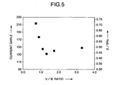
- the growth conditions of base layer 43 were as follows. Growth temperature: 620°C; raw material of Group III: trimethylgallium (TMG); raw material of Group V: arsine (AsH 3 ); dopant for forming p-type base layer: CBrCl 3 ; and V/III ratio: 0.9. Under the above growth conditions, the carrier concentration of the base layer 43 of 3.6 ⁇ 10 19 cm -3 was obtained by adjusting the doping amount of C as a dopant. The current gain ⁇ of the HBT device in this case was measured to obtain 180. Further, a ratio of current gain ⁇ /base sheet resistance BRs was measured to obtain 0.60.
- An HBT device was produced under the same conditions as in Example 1, except that the V/III ratio was 0.7, and the current gain P of the HBT device was measured to obtain 215. Further, the life time of minority carriers in the base layer 43 was measured to obtain 230 psec. The ratio of current gain ⁇ /base sheet resistance BRs was measured to obtain 0.70.
- HBT devices for comparison were produced under the same growth conditions as in Example 1, except that the V/III ratio was 1.3, 3.3 or 25 which was more than 1.0.
- the current gains ⁇ were all 150. Furthermore, The ratio of current gain ⁇ /base sheet resistance BRs was measured to obtain 0.50. The life time of minority carriers in the case of the V/III ratio being 25 was measured to obtain 160 psec.
- FIG. 5 and FIG. 6 show the results of the measurements. Under such conditions as giving a growth determined by Group V gas flow rate-feed where the V/III ratio was not more than 1.0, the life time of minority carriers in the base layer was prolonged because of good crystalline quality. It is considered that for this reason, ⁇ was improved.
- the growth conditions of the base layer are those which give a growth determined by a Group V gas flow rate-feed
- crystallinity of the base layer can be improved, life time of minority carriers can be prolonged, and, furthermore, current gain can be markedly improved by using a high ratio of current gain ⁇ /base sheet resistance BRs.
- the carrier concentration of the base layer can be controlled independently of the growth conditions, the carrier concentration can be easily controlled to the desired value.
- Devices using the compound semiconductor wafer of the present invention are used as HBT in the frequency area higher than microwave band.
Abstract
Description
| V/III ratio | β/BRs | τ (ps) | |
| Comparative Example | 25 | 0.50 | 160 |
| Example 1 | 0.9 | 0.60 | 200 |
| Example 2 | 0.7 | 0.70 | 230 |
Claims (6)
- A method for producing a compound semiconductor wafer used for production of HBT by vapor growth of a sub-collector layer, a collector layer, a base layer and an emitter layer in this order on a compound semiconductor substrate using MOCVD method wherein the base layer is a p-type compound semiconductor thin film layer containing at least one of Ga, Al and In as a Group III element and As as a Group V element and is grown under such conditions that the growth rate gives a growth determined by a Group V gas flow rate-feed.
- A method according to claim 1, wherein the base layer is grown with the V/III ratio being within the range of 0.3-1.0.
- A method according to claim 1 or 2, wherein the adjustment of carrier concentration in the base layer is controlled by the flow rate of methane halide.
- A method according to claim 1 or 2, wherein the adjustment of carrier concentration in the base layer is controlled by the flow rate of CBrCl3.
- A compound semiconductor device comprising a sub-collector layer, a collector layer, a base layer and an emitter layer formed as thin film crystal layers in this turn on a compound semiconductor substrate by vapor growth wherein the life time of minority carriers in the base layer is not less than 200 psec.
- A compound semiconductor device containing a hetero junction bi-polar transistor comprising a sub-collector layer, a collector layer, a base layer and an emitter layer formed as thin film crystal layers in this turn on a compound semiconductor substrate by vapor growth wherein the ratio of current gain/base sheet resistance of the hetero junction bi-polar transistor is not less than 0.60.
Applications Claiming Priority (3)
| Application Number | Priority Date | Filing Date | Title |
|---|---|---|---|
| JP2002233708A JP2004079574A (en) | 2002-08-09 | 2002-08-09 | Method for manufacturing compound semiconductor wafer and compound semiconductor element |
| JP2002233708 | 2002-08-09 | ||
| PCT/JP2003/009818 WO2004015781A1 (en) | 2002-08-09 | 2003-08-01 | Method for manufacturing compound semiconductor wafer and compound semiconductor device |
Publications (2)
| Publication Number | Publication Date |
|---|---|
| EP1542288A1 true EP1542288A1 (en) | 2005-06-15 |
| EP1542288A4 EP1542288A4 (en) | 2008-05-21 |
Family
ID=31711872
Family Applications (1)
| Application Number | Title | Priority Date | Filing Date |
|---|---|---|---|
| EP03784504A Withdrawn EP1542288A4 (en) | 2002-08-09 | 2003-08-01 | COMPOSITE SEMICONDUCTOR DEVICE AND METHOD FOR MANUFACTURING THE SAME |
Country Status (7)
| Country | Link |
|---|---|
| US (2) | US7208387B2 (en) |
| EP (1) | EP1542288A4 (en) |
| JP (1) | JP2004079574A (en) |
| KR (1) | KR100990350B1 (en) |
| AU (1) | AU2003252335A1 (en) |
| TW (1) | TW200402766A (en) |
| WO (1) | WO2004015781A1 (en) |
Families Citing this family (6)
| Publication number | Priority date | Publication date | Assignee | Title |
|---|---|---|---|---|
| US7935616B2 (en) * | 2004-06-17 | 2011-05-03 | Burgener Ii Robert H | Dynamic p-n junction growth |
| JP2006185990A (en) * | 2004-12-27 | 2006-07-13 | Renesas Technology Corp | Semiconductor device, method for manufacturing the same, and electronic device |
| US8193609B2 (en) * | 2008-05-15 | 2012-06-05 | Triquint Semiconductor, Inc. | Heterojunction bipolar transistor device with electrostatic discharge ruggedness |
| JP5507975B2 (en) * | 2009-11-19 | 2014-05-28 | 住友化学株式会社 | Semiconductor substrate, electronic device, and method for manufacturing semiconductor substrate |
| CN106435522B (en) * | 2016-09-27 | 2019-04-12 | 中国电子科技集团公司第四十八研究所 | The PECVD depositing operation of crystal silicon solar battery aluminum oxide passivation film |
| US12675267B2 (en) | 2023-11-15 | 2026-07-07 | International Business Machines Corporation | Program code optimization using iterative application of machine learning model |
Family Cites Families (9)
| Publication number | Priority date | Publication date | Assignee | Title |
|---|---|---|---|---|
| JPS5792526A (en) | 1980-11-28 | 1982-06-09 | Toshiba Corp | Vaper growth of compound semiconductor |
| JP2885435B2 (en) | 1989-09-25 | 1999-04-26 | 株式会社東芝 | Method for manufacturing compound semiconductor thin film |
| EP0390552B1 (en) * | 1989-03-31 | 1995-12-20 | Kabushiki Kaisha Toshiba | Method of manufacturing compound semiconductor thin film |
| JPH06236852A (en) | 1993-02-12 | 1994-08-23 | Matsushita Electron Corp | Semiconductor device and manufacture thereof |
| JP2000049094A (en) | 1998-07-27 | 2000-02-18 | Sumitomo Chem Co Ltd | Method for manufacturing compound semiconductor |
| JP2000068284A (en) * | 1998-08-19 | 2000-03-03 | Sharp Corp | Method of manufacturing heterojunction bipolar transistor and power amplifier |
| JP4126812B2 (en) * | 1999-07-07 | 2008-07-30 | 富士ゼロックス株式会社 | Optical semiconductor device |
| US6847060B2 (en) * | 2000-11-27 | 2005-01-25 | Kopin Corporation | Bipolar transistor with graded base layer |
| KR100469642B1 (en) * | 2002-05-31 | 2005-02-02 | 한국전자통신연구원 | Photoreceiver of wavelength selective detection and method of manufacturing the same |
-
2002
- 2002-08-09 JP JP2002233708A patent/JP2004079574A/en active Pending
-
2003
- 2003-08-01 KR KR1020057002270A patent/KR100990350B1/en not_active Expired - Fee Related
- 2003-08-01 WO PCT/JP2003/009818 patent/WO2004015781A1/en not_active Ceased
- 2003-08-01 EP EP03784504A patent/EP1542288A4/en not_active Withdrawn
- 2003-08-01 AU AU2003252335A patent/AU2003252335A1/en not_active Abandoned
- 2003-08-01 US US10/524,013 patent/US7208387B2/en not_active Expired - Lifetime
- 2003-08-06 TW TW092121492A patent/TW200402766A/en not_active IP Right Cessation
-
2007
- 2007-03-19 US US11/688,166 patent/US7576352B2/en not_active Expired - Lifetime
Also Published As
| Publication number | Publication date |
|---|---|
| AU2003252335A1 (en) | 2004-02-25 |
| TWI312534B (en) | 2009-07-21 |
| KR100990350B1 (en) | 2010-10-29 |
| US7576352B2 (en) | 2009-08-18 |
| US20060001044A1 (en) | 2006-01-05 |
| TW200402766A (en) | 2004-02-16 |
| US20070170466A1 (en) | 2007-07-26 |
| AU2003252335A8 (en) | 2004-02-25 |
| KR20050060064A (en) | 2005-06-21 |
| US7208387B2 (en) | 2007-04-24 |
| EP1542288A4 (en) | 2008-05-21 |
| JP2004079574A (en) | 2004-03-11 |
| WO2004015781A1 (en) | 2004-02-19 |
Similar Documents
| Publication | Publication Date | Title |
|---|---|---|
| US6849862B2 (en) | III-V compound semiconductor device with an AlxByInzGa1-x-y-zN1-a-bPaAsb non-continuous quantum dot layer | |
| US20020022286A1 (en) | Method for growing p-n heterojunction-based structures utilizing HVPE techniques | |
| US6555452B2 (en) | Method for growing p-type III-V compound material utilizing HVPE techniques | |
| US7576352B2 (en) | Method for producing compound semiconductor wafer and compound semiconductor device | |
| US6599133B2 (en) | Method for growing III-V compound semiconductor structures with an integral non-continuous quantum dot layer utilizing HVPE techniques | |
| US20020047127A1 (en) | P-N homojunction-based structures utilizing HVPE grown III-V compound layers | |
| US20020030192A1 (en) | III-V compounds semiconductor device with an AIxByInzGa1-x-y-zN non continuous quantum dot layer | |
| US6559467B2 (en) | P-n heterojunction-based structures utilizing HVPE grown III-V compound layers | |
| WO2007116517A1 (en) | Compound semiconductor structure and process for producing the same | |
| US6472300B2 (en) | Method for growing p-n homojunction-based structures utilizing HVPE techniques | |
| US20020017650A1 (en) | III-V compound semiconductor device with an InGaN1-x-yPxASy non-continuous quantum dot layer | |
| CN117766389A (en) | Heterojunction bipolar transistor and MOCVD epitaxial growth method thereof | |
| US20020047135A1 (en) | P-N junction-based structures utilizing HVPE grown III-V compound layers | |
| JP2885435B2 (en) | Method for manufacturing compound semiconductor thin film | |
| KR101082773B1 (en) | Compound semiconductor device and its manufacturing method | |
| JP2006216864A (en) | Compound semiconductor manufacturing equipment | |
| JP2004241463A (en) | Compound semiconductor vapor phase growth method | |
| JP5543302B2 (en) | Compound semiconductor wafer manufacturing method and compound semiconductor device | |
| JPH07201761A (en) | Method for growing compound semiconductor | |
| JP2003303825A (en) | Method for manufacturing compound semiconductor wafer and compound semiconductor element | |
| JPH0590160A (en) | Crystal growth method | |
| JP2793239B2 (en) | Method for manufacturing compound semiconductor thin film | |
| JP2004134548A (en) | Method of manufacturing heterojunction bipolar transistor | |
| JP5507975B2 (en) | Semiconductor substrate, electronic device, and method for manufacturing semiconductor substrate | |
| JPH05190467A (en) | Manufacture of epitaxial wafer |
Legal Events
| Date | Code | Title | Description |
|---|---|---|---|
| PUAI | Public reference made under article 153(3) epc to a published international application that has entered the european phase |
Free format text: ORIGINAL CODE: 0009012 |
|
| 17P | Request for examination filed |
Effective date: 20050225 |
|
| AK | Designated contracting states |
Kind code of ref document: A1 Designated state(s): AT BE BG CH CY CZ DE DK EE ES FI FR GB GR HU IE IT LI LU MC NL PT RO SE SI SK TR |
|
| AX | Request for extension of the european patent |
Extension state: AL LT LV MK |
|
| DAX | Request for extension of the european patent (deleted) | ||
| RBV | Designated contracting states (corrected) |
Designated state(s): DE FR GB |
|
| A4 | Supplementary search report drawn up and despatched |
Effective date: 20080423 |
|
| 17Q | First examination report despatched |
Effective date: 20101111 |
|
| STAA | Information on the status of an ep patent application or granted ep patent |
Free format text: STATUS: THE APPLICATION IS DEEMED TO BE WITHDRAWN |
|
| 18D | Application deemed to be withdrawn |
Effective date: 20110322 |