TECHNICAL FIELD
The present invention relates to a semiconductor memory which requires periodic
refresh operations to retain data written in its memory cells. In particular, the present
invention relates to a semiconductor memory which performs refresh operations
automatically inside without requiring a refresh command from exterior. In addition, the
present invention relates to a technology for testing the foregoing semiconductor memory.
TECHNOLOGICAL BACKGROUND
In recent years, mobile apparatuses such as a cellular phone have become more
sophisticated in service facilities, and the amounts of data to be handled have been growing
steadily. Higher capacities are then required of the work memories to be mounted on the
mobile apparatuses accordingly.
Conventionally, the work memories of the mobile apparatuses have used SRAMs
which allow easier system configuration. The SRAMs are, however, greater than DRAMs in
the number of devices for constituting each single bit of cell, and thus are disadvantageous
for higher capacities. In view of this, semiconductor memories that have DRAM memory
cells and operate as SRAMs by performing refresh operations on the memory cells
automatically inside have been developed.
In the semiconductor memories of this type, the refresh operation time for
performing a single refresh operation is included in the read cycle time or write cycle time.
Specifically, the first half of a cycle time is allocated for the refresh operation time. The
actual read operation or write operation is performed in the second half of the cycle time.
Thus, the systems (users) on which the semiconductor memories are mounted need not be
aware of the refresh operations in the semiconductor memories. That is, the users can use
these semiconductor memories as SRAMs.
Besides, in the semiconductor memories of this type, the refresh operation time is
rendered shorter than the read operation time for the sake of reducing the cycle time.
Specifically, the time for selecting word lines in a refresh operation is shorter than the time
for selecting word lines in a read operation (for example, see Japanese Examined Patent
Application Publication No. 7-58589 (pp. 2-3, Fig. 4)).
In the semiconductor memory disclosed in the foregoing publication, a refresh
operation is performed before a read operation when a refresh request occurs immediately
before the read operation. The refresh operation time is set to be shorter than the read
operation time. The refresh operation time, however, can only be made slightly shorter
than the read operation time in order to rewrite predetermined signal quantities of data to
the memory cells. As described above, an actual read operation is performed in the second
half of the read cycle time. Consequently, it is impossible to reduce the access time
sufficiently.
Incidentally, Fig. 4 of the foregoing publication does not show that refresh
operations RF are performed before and after a read operation (read data D). What is
shown in Fig. 4 is a simplified example where the refresh operation RF is performed before
or after the read operation in accordance with the timing of occurrence of the refresh
request (lines 1-10 in column 5 of the foregoing publication).
Moreover, as stated above, the pseudo SRAMs perform refresh operations
automatically without being recognized from exterior. In the meantime, the data retained
in the memory cells might be corrupted unless refresh operations are performed properly.
It is therefore necessary to evaluate if refresh operations are performed properly. In
particular, detailed evaluations are required of the circuit operation when a conflict occurs
between a request for a read operation or write operation which is supplied from exterior
and a request for a refresh operation which occurs inside the chips.
DISCLOSURE OF THE INVENTION
It is an object of the present invention to provide a semiconductor memory which
has both the high capacity of a DRAM and the usability of an SRAM.
It is another object of the present invention to reduce the access time of a
semiconductor memory which performs refresh operations automatically inside the chip.
It is another object of the present invention to perform reliable refresh operations
in a semiconductor memory which performs the refresh operations automatically inside the
chip.
It is another object of the present invention to evaluate the internal state of the chip
for the sake of performing reliable refresh operations.
According to a first aspect of the semiconductor memory of the present invention,
a memory core has a plurality of memory cells. A command control circuit outputs an
access signal for accessing the memory cells in response to an access request supplied
through a command terminal. A refresh timer generates a refresh request at
predetermined cycles in order to refresh the memory cells. A refresh control circuit
outputs a first refresh signal in response to the refresh request in order to start a refresh
operation. The output of the first refresh signal is stopped when a conflict occurs between
the access request and the refresh request. Consequently, an access operation
corresponding to the access request can be started earlier. That is, it is possible to reduce
the access time. The refresh control circuit outputs a second refresh signal in response to
the refresh request after the access operation corresponding to the access request. A core
control circuit performs the access operation in response to the access signal, and performs
first and second refresh operations in response to the first and second refresh signals,
respectively. The second refresh operation is always performed after the first refresh
operation. Thus, even if the first refresh operation only rewrites the memory cells
insufficiently, sufficient signal quantities of data are rewritten to the memory cells by the
subsequent second refresh operation. Consequently, even when a conflict occurs between
the access request and the refresh request and precedence is given to the access request, it
is possible to retain the data in the memory cells with reliability.
According to a preferred example of the first aspect of the semiconductor memory
of the present invention, an external address input circuit receives an external address
signal through an address terminal. A refresh counter generates a refresh address signal
indicating a memory cell to refresh out of the memory cells. A switch circuit selects the
refresh address in response to the output of the first and second refresh signals, selects the
external address signal when neither of the first and second refresh signals is output, and
outputs the selected address signal to the memory core. Since the switch circuit is
operated by the first and second refresh signals, it is possible to simplify the switching
control on the address signals. Consequently, the switch circuit can be configured simply.
According to a preferred example of the first aspect of the semiconductor memory
of the present invention, the execution time of the first refresh operation is shorter than the
execution time of the second refresh operation. The execution time of the first refresh
operation can be minimized to start the access operation even earlier.
According to a preferred example of the first aspect of the semiconductor memory
of the present invention, the execution time of the first refresh operation is the time in
which data to be rewritten to the memory cells by the first refresh operation is amplified to
a signal quantity capable of being retained without loss until the second refresh operation is
performed. That is, the execution time of the first refresh operation is set to its minimum.
Since the execution time of the first refresh operation is minimized, the access operation
can be started even earlier.
According to a preferred example of the first aspect of the semiconductor memory
of the present invention, the memory core includes a plurality of word lines connected to
the memory cells, respectively, a bit line connected to the memory cells, and a sense
amplifier connected to the bit line. The first and second refresh operations include a read
stage, an amplifying stage, and a precharging stage. In the read stage, data is read to the
bit line from a memory cell accessed in response to the selection of any one of the word
lines. In the amplifying stage, the sense amplifier is activated after the data is read to the
bit line, and the data on the bit line is amplified. The amplified data is rewritten to the
accessed memory cell. In the precharging stage, the word lines are deselected, and the bit
line is precharged to a predetermined voltage.
The read stages of the first and second refresh operations are identical to each
other in time. The precharging stages of the first and second refresh operations are
identical to each other in time. The time of the amplifying stage of the first refresh
operation is shorter than the time of the amplifying stage of the second refresh operation.
The execution time of the first refresh operation can be minimized easily by adjusting the
time of the amplifying stage alone in accordance with the operation. That is, such circuits
as the core control circuit can be configured simply.
According to a preferred example of the first aspect of the semiconductor memory
of the present invention, the refresh control circuit masks the output of the first refresh
signal and outputs the second refresh signal alone when no conflict occurs between the
access request and the refresh request. Since the first refresh operation is performed only
when needed, it is possible to reduce the power consumption during operation.
According to a preferred example of the first aspect of the semiconductor memory
of the present invention, the sum of the execution times of the first and second refresh
operations and the execution time twice that of the access operation is smaller than twice
the minimum interval of supply of the access request, or an external access cycle time. In
other words, the first and second refresh operations and two access operations can be
performed within two external access cycle times. In the present invention, the execution
time of the first refresh operation is short as described above. It is therefore possible to
reduce the external access cycle as compared to heretofore.
According to a preferred example of the first aspect of the semiconductor memory
of the present invention, the execution time of the second refresh operation is the same as
the execution time of the access operation. This makes it possible to share the control
circuits for performing the second refresh operation and the access operation. As a result,
the core control circuit and the like can be reduced in circuit scale.
According to a preferred example of the first aspect of the semiconductor memory
of the present invention, the execution time of the second refresh operation is shorter than
the execution time of the access operation. This produces a timing margin between the
execution of the second refresh operation and the execution of the next access operation.
Consequently, the core control circuit and the like can be improved in operation margin,
whereby the timing design of these circuits is facilitated.
According to a preferred example of the first aspect of the semiconductor memory
of the present invention, a test control circuit generates first and second refresh signals
from a test refresh request signal supplied through an external testing probe in a test mode.
Consequently, a second refresh operation to be performed after a first refresh operation can
be started at desired timing. The data to be retained in the memory cells by the first
refresh is rewritten to the memory cells again by the second refresh operation. The
operation margin of the first refresh operation can thus be evaluated easily.
According to a preferred example of the first aspect of the semiconductor memory
of the present invention, the test control circuit sets the interval of generation of the first
and second refresh signals in accordance with the pulse width of the test refresh request
signal. Consequently, the interval of generation of the first and second refresh signals can
be set freely from the one single external testing probe.
According to a second aspect of the semiconductor memory of the present
invention, a memory core has a plurality of memory cells, a bit line connected to the
memory cells, and a sense amplifier connected to the bit line. A command control circuit
outputs an access control signal for accessing the memory cells in response to an access
request supplied through a command terminal. An operation control circuit makes the
memory core perform an access operation in response to the access control signal.
A refresh timer generates an internal refresh request at predetermined cycles. A
refresh control circuit outputs either one of a first refresh control signal and a second
refresh control signal in accordance with the timing of occurrence of the access request and
the internal refresh request. That is, the refresh control circuit switches between the
outputs of the first and second refresh control signals in accordance with the timing of
occurrence of the access request and the internal refresh request. The sense amplifier is
activated by the first refresh control signal for a first period, and is activated by the second
refresh control signal for a second period longer than the first period. An operation control
circuit makes the memory core perform first and second refresh operations in response to
the first and second refresh control signals. In this way, the semiconductor memory
performs two types of refresh operations automatically in accordance with the refresh
requests it generates, without being recognized from exterior.
A detecting circuit operates in a test mode and outputs a detecting signal when it
detects the first refresh control signal. Consequently, the timing of switch between the
first and second refresh control signals by the refresh control circuit can be detected from
the output of the detecting signal. That is, even if the semiconductor memory has the two
types of refresh operation facilities, it is possible to evaluate the timing conditions under
which the respective refresh operations are performed. Besides, for example, when the
first refresh control signal can occur consecutively to cause an operation failure, it is
possible to evaluate the timing of occurrence of the failure from the detecting signal with
reliability.
Since the two types of refresh operations performed automatically inside the
semiconductor memory can be detected easily, it is possible to evaluate the semiconductor
memory for operation characteristics pertaining to these refresh operations accurately by
simple techniques. As a result, it is possible to reduce the evaluation time with a reduction
in the development period of the semiconductor memory. That is, the development cost
can be reduced. In another respect, when failures occur from variations of the
manufacturing conditions or the like of mass-produced semiconductor memories, it is
possible to conduct a failure analysis promptly and minimize the period of dropped yields.
According to a preferred example of the second aspect of the semiconductor
memory of the present invention, the detecting signal detected by the detecting circuit is
output to exterior of the semiconductor memory through an external terminal.
Consequently, it is possible to evaluate the semiconductor memory for operation
characteristics pertaining to the refresh operations accurately, for example, by detecting the
detecting signal with an evaluation apparatus for evaluating the refresh characteristics of
the semiconductor memory.
According to a preferred example of the second aspect of the semiconductor
memory of the present invention, a tristate output buffer outputs read data from the
memory cells to the data terminal. An output mask circuit controls the tristate output
buffer in the test mode, thereby prohibiting the output of the read data to the data terminal
in response to the detecting signal and setting the data terminal to a high impedance state.
Thus, the evaluation apparatus connected to the semiconductor memory can detect the
detecting signal by measuring the data signal for the high impedance state. For example,
the occurrence of the detecting signal can be detected easily by using an LSI tester as the
evaluation apparatus and conducting a pass/fail evaluation through the use of a program
for evaluating the access time. That is, the semiconductor memory can be easily evaluated
for operation characteristics pertaining to the refresh operations. Moreover, the use of the
data terminal as the external terminal can eliminate the need for the formation of a new
terminal, thereby avoiding an increase in chip size.
According to a preferred example of the second aspect of the semiconductor
memory of the present invention, a refresh selection circuit outputs a test refresh request
supplied through an external testing probe, instead of the internal refresh request, to the
refresh control circuit in the test mode. Here, the internal refresh request output from the
refresh timer is masked. It is therefore possible to supply refresh requests of desired
timing from exterior of the semiconductor memory. Since the refresh request and the
access request can be supplied from a single evaluation apparatus, it is possible to control
the deviation (time difference) between the access request and the refresh request with high
precision. As a result, the semiconductor memory can be evaluated for operation
characteristics pertaining to the refresh operations in detail.
According to a preferred example of the second aspect of the semiconductor
memory of the present invention, the refresh timer receives a refresh adjustment signal for
changing the cycle of generation of the refresh request in the test mode. It is therefore
possible to generate refresh requests of desired timing inside the semiconductor memory
by using circuits that operate in a normal operation. The refresh characteristics can thus
be evaluated under the same condition as in actual circuit operations of the semiconductor
memory.
According to a preferred example of the second aspect of the semiconductor
memory of the present invention, an arbiter in the refresh control circuit decides precedence
between an access operation corresponding to the access request and a refresh operation
corresponding to the refresh request when a conflict occurs between the access request and
the internal refresh request. The arbiter outputs the access control signal and then the
second refresh control signal when the access request has precedence over the internal
refresh request. Besides, the arbiter outputs the first refresh control signal, the access
control signal, and the second refresh control signal in succession when the internal refresh
request has precedence over the access request.
The refresh operation corresponding to the first refresh control signal ends in a
short time. Thus, even when the internal refresh request has precedence over the access
request, the access operation corresponding to the access request can be started early.
That is, it is possible to reduce the access time. The refresh operation corresponding to
the second refresh control signal is always performed after the refresh operation
corresponding to the first refresh control signal (the first refresh operation). Thus, even if
the first refresh operation only rewrites the memory cells insufficiently, sufficient signal
quantities of data are rewritten to the memory cells by the subsequent refresh operation.
Consequently, even when a conflict occurs between an access request and the refresh
request and precedence is given to the access request, it is possible to retain the data in the
memory cells with reliability.
According to a preferred example of the second aspect of the semiconductor
memory of the present invention, the execution time of the first refresh operation is the
time in which data to be rewritten to the memory cells by the first refresh operation is
amplified to a signal quantity capable of being retained without loss until the second refresh
operation is performed. That is, the execution time of the first refresh operation is set to
its minimum. Since the execution time of the first refresh operation is minimized, the
access operation can be started even earlier.
According to a third aspect of the semiconductor memory of the present invention,
a memory core has a plurality of memory cells. An external terminal receives an access
request for accessing the memory cells. A refresh timer generates a refresh request at
predetermined cycles. A core control circuit sets the end time of a refresh operation
corresponding to the refresh request to between a first time and a second time later than
the first time in accordance with the timing of supply of the access request when a conflict
occurs between the access request and the refresh request and precedence is given to the
refresh request. For example, the core control circuit sets the end time to an earlier time if
a difference between the time of reception of the access request and the time of occurrence
of the refresh request is small. Moreover, the core control circuit sets the end time to a
later time if the difference between the time of reception of the access request and the time
of occurrence of the refresh request is large. The end time of the refresh operation is not
fixed but variable depending on the timing of supply of the access request. Consequently,
when a conflict occurs between the refresh request and the access request, it is possible to
start the access request even earlier after the refresh operation. That is, the access time
can be reduced further.
Since the end time of the refresh operation varies in accordance with the timing of
supply of the access request, the access time remains unchanged even if the access request
gradually deviates from the refresh request. It is therefore possible to prevent the access
time from varying with the time difference between the refresh request and the access
request. Since the access time makes no variation, it is possible to make the maximum
value (worst value) of the access time smaller.
According to a preferred example of the third aspect of the semiconductor memory
of the present invention, an arbiter decides precedence between an access operation
corresponding to the access request and a refresh operation corresponding to the refresh
request when a conflict occurs between the access request and the internal refresh request.
The arbiter outputs an access control signal for starting an access operation and then a
refresh control signal for starting a refresh operation to the core control circuit when the
access request has precedence over the refresh request. Moreover, the arbiter outputs the
refresh control signal and then the access control signal to the core control circuit when the
refresh request has precedence over the access request. The core control circuit performs
the access operation and the refresh operation in accordance with the access control signal
and the refresh control signal, respectively. Consequently, the access operation and the
refresh operation can be performed with reliability even when a conflict occurs between the
access request and the refresh request.
According to a preferred example of the third aspect of the semiconductor memory
of the present invention, the memory core has a plurality of word lines connected to the
memory cells, respectively. The end time of the refresh operation corresponds to the time
of inactivation of the word lines. That is, the core control circuit ends the refresh operation
by inactivating the word lines in accordance with the timing of supply of the access request.
According to a preferred example of the third aspect of the semiconductor memory
of the present invention, the memory core has a bit line connected to the memory cells and
a sense amplifier connected to the bit line. The end time of the refresh operation
corresponds to the time of inactivation of the sense amplifier. That is, the core control
circuit ends the refresh operation by inactivating the sense amplifier as well as inactivating
the word lines in accordance with the timing of supply of the access request.
According to a preferred example of the third aspect of the semiconductor memory
of the present invention, the core control circuit has a timing generator for generating a first
time signal for notifying of the first time and a second time signal for notifying of the
second time. The core control circuit sets the end time in accordance with the timing of
supply of the access request with respect to the timing of generation of the first and second
time signals. Consequently, the refresh operation can be ended in accordance with the
timing of supply of the access request by using a simple logic circuit.
According to a preferred example of the third aspect of the semiconductor memory
of the present invention, the end time is set to the first time and a first short refresh
operation is performed when the access request is supplied before the first time. The end
time is set to the time of supply of the access request and a second short refresh operation
is performed when the access time is supplied between the first time and the second time.
The end time is set to the second time and a normal short refresh operation is performed
when the access request is supplied after the second time.
The refresh operation always ends at or after the first time. Since the minimum
refresh operation period is secured (the first short refresh operation), it is possible to
prevent the data in the memory cells from being corrupted by the refresh operation.
Besides, the refresh operation always ends at or before the second time. Even when no
access request is supplied, the refresh operation is always terminated at the second time.
The memory core can thus be prevented from unnecessary operations. As a result, it is
possible to avoid unnecessary consumption of the core operation current. In addition,
when the refresh operation is set to end between the first time and the second time, it is
possible to complete the refresh operation in synchronization with the timing of supply of
the access request. Here, the memory cells are written with maximum charges capable of
being rewritten without deterioration in access time. This allows a margin for the data
retention characteristics as compared to the case of the first short refresh operation.
According to a preferred example of the third aspect of the semiconductor memory
of the present invention, the memory core has a plurality of word lines connected to the
memory cells. The semiconductor memory has a first operation mode in which the interval
of generation of the refresh request to be output from the refresh timer is longer, and a
second operation mode in which the interval of generation of the refresh request is shorter.
One of the word lines is selected in response to the refresh request.
In the first operation mode, when the first or second short refresh operation is
performed in response to the refresh request, the semiconductor memory attempts the
normal refresh operation on the selected word line after this first or second refresh
operation. The semiconductor memory enters the second operation mode when the access
request has precedence and the normal refresh operation on the selected word line cannot
be performed before the next refresh request occurs. Since the decision on the entry to
the second operation mode is postponed for a predetermined period, whether the frequency
of supply of the access request is temporarily high or remains high can be decided with
reliability. It is therefore possible to enter an optimum operation mode in accordance with
the access frequency. As a result, the period of being in the second operation mode can be
minimized to make the power consumption of the refresh operation the bare minimum.
That is, the semiconductor memory can be reduced in power consumption.
According to a preferred example of the third aspect of the semiconductor memory
of the present invention, a refresh counter makes a count operation in response to the
refresh request in order to select the word lines in succession. The semiconductor memory
enters the first operation mode when the normal refresh operation alone is performed and
the refresh counter goes through a single round in the second operation mode. When the
frequency of the access request falls for a predetermined period, the first operation mode is
entered to lower the frequency of the refresh request. This allows a reduction in power
consumption.
BRIEF DESCRIPTION OF THE DRAWINGS
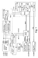
Fig. 1 is a block diagram showing a first embodiment of the semiconductor
memory of the present invention;
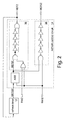
Fig. 2 is a block diagram showing the details of the refresh control circuit shown in
Fig. 1;
Fig. 3 is a circuit diagram showing the details of essential parts of the core control
circuit shown in Fig. 1;
Fig. 4 is a circuit diagram showing the details of the refresh address input circuit,
the external address input circuit, and the switch circuit shown in Fig. 1;
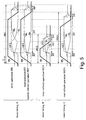
Fig. 5 is a timing chart showing the basic operation of the memory cell array
according to the first embodiment;
Fig. 6 is a timing chart showing an example of operation of the first embodiment;
Fig. 7 is a timing chart showing another example of operation of the first
embodiment;
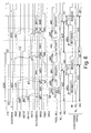
Fig. 8 is a timing chart showing another example of operation of the first
embodiment;
Fig. 9 is a block diagram showing a second embodiment of the semiconductor
memory of the present invention;
Fig. 10 is a circuit diagram showing the details of essential parts of the core control
circuit shown in Fig. 9;
Fig. 11 is a timing chart showing an example of operation of the second
embodiment;
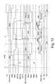
Fig. 12 is a timing chart showing another example of operation of the second
embodiment;
Fig. 13 is a block diagram showing a third embodiment of the semiconductor
memory of the present invention;
Fig. 14 is a block diagram showing the details of the refresh control circuit shown
in Fig. 13;
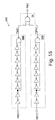
Fig. 15 is a circuit diagram showing the details of the core control circuit shown in
Fig. 13;
Fig. 16 is a timing chart showing an example of operation of the third embodiment;
Fig. 17 is a timing chart showing another example of operation of the third
embodiment;
Fig. 18 is a block diagram showing a fourth embodiment of the semiconductor
memory of the present invention;
Fig. 19 is a circuit diagram showing the details of the refresh decision circuit shown
in Fig. 18;
Fig. 20 is a circuit diagram showing the details of the data output circuit shown in
Fig. 18;
Fig. 21 is a timing chart showing the basic operation of the memory cell array
according to the fourth embodiment;
Fig. 22 is a timing chart showing an example of operation of the fourth
embodiment in a normal operation mode;
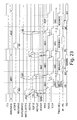
Fig. 23 is a timing chart showing another example of operation of the fourth
embodiment in the normal operation mode;
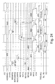
Fig. 24 is a timing chart showing another example of operation of the fourth
embodiment in the normal operation mode;
Fig. 25 is a timing chart showing an example of operation of the fourth
embodiment in a first test mode;
Fig. 26 is a timing chart showing an example of operation of the fourth
embodiment in a second test mode;
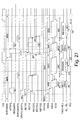
Fig. 27 is a timing chart showing an example of operation of the fourth
embodiment in the second test mode;
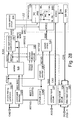
Fig. 28 is a block diagram showing a fifth embodiment of the semiconductor
memory of the present invention;
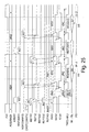
Fig. 29 is a block diagram showing a sixth embodiment of the semiconductor
memory of the present invention;
Fig. 30 is a timing chart showing an example of operation of the sixth embodiment
in a test mode;
Fig. 31 is a block diagram showing a seventh embodiment of the semiconductor
memory of the present invention;
Fig. 32 is a circuit diagram showing the details of essential parts of the core control
circuit shown in Fig. 31;
Fig. 33 is a block diagram showing a precedence decision circuit which is formed
inside the core control circuit;
Fig. 34 is a timing chart showing an example of operation of the seventh
embodiment;
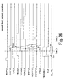
Fig. 35 is a timing chart showing another example of operation of the seventh
embodiment;
Fig. 36 is a timing chart showing another example of operation of the seventh
embodiment;
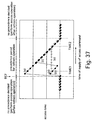
Fig. 37 is a characteristic chart showing the access time for situations where a
conflict occurs between an access request and a refresh request;
Fig. 38 is a timing chart showing a shift from a first operation mode to a second
operation mode according to the seventh embodiment; and
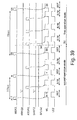
Fig. 39 is a timing chart showing a shift from the second operation mode to the
first operation mode according to the seventh embodiment.
BEST MODE FOR CARRYING OUT THE INVENTION
Hereinafter, embodiments of the present invention will be described with reference
to the drawings. In the drawings, thick lines represent signal lines each consisting of a
plurality of bits. Double circles in the drawings represent external terminals. Signals with
a leading "/" and signals ending in "X" show negative logic. Signals ending in "Z" show
positive logic.
Fig. 1 shows a first embodiment of the semiconductor memory of the present
invention. This semiconductor memory is formed as a pseudo SRAM which has DRAM
memory cells and an SRAM interface. The pseudo SRAM performs periodic refresh
operations inside the chip without receiving refresh commands from exterior, thereby
retaining data written in its memory cells. This pseudo SRAM is used, for example, as a
work memory to be mounted on a cellular phone.
The pseudo SRAM has a command control circuit 10, a refresh timer 12, a refresh
control circuit 14, a refresh counter 16, a refresh address input circuit 18, an external
address input circuit 20, a switch circuit 22, a data input/output circuit 24, a core control
circuit 26, and a memory core 28.
The command control circuit 10 receives command signals (a chip enable signal
/CE, an output enable signal /OE, and a write enable signal /WE) from exterior through
command terminals, decodes the received commands, and outputs a read control signal
RDZ, a write control signal WRZ (access signal), and read/write control signals RWZ and
RWIZ (access signals). The read control signal RDZ and the write control signal WRZ (high
level) are output when a read command and a write command are supplied, respectively.
The read/write control signals RWZ and RWIZ (high level) are output when the read
command and the write command are supplied. The read/write control signal RWIZ is
output earlier than the read /write control signal RWZ.
The refresh timer 12 outputs a refresh request signal REFI0Z (refresh command) at
predetermined cycles. The refresh request signal REFI0Z is generated at cycles such that
memory cells MC can be refreshed in succession without losing the data retained in the
memory cells MC. For example, the cycle of generation of the refresh request signal REFIOZ
is set so that all the memory cells MC are refreshed once within 64 ms. Specifically, when
there are arranged 2048 word lines WL to be selected in succession by respective refresh
requests, the refresh request signal REFIOZ is generated at every 31 µs.
The refresh control circuit 14 outputs a refresh signal REFSZ (first refresh signal)
and a refresh signal REFZ (second refresh signal) in accordance with the read/write control
signals RWZ and RWIZ and the refresh request signal REFI0Z. The refresh counter 16
makes a count operation a certain period after the rising edge of the refresh signal REFZ,
and outputs a refresh address signal RAZ successively.
The refresh address input circuit 18 outputs the refresh address signal RAZ as a
refresh address signal REFAD. The external address input circuit 20 receives an address
signal ADD through an address terminal, and outputs the received signal as a row address
signal RAD (upper address) and a column address signal CAD (lower address). Note that
the pseudo SRAM is a memory of address non-multiplex type which receives the upper
address and the lower address simultaneously.
The switch circuit 22 outputs the refresh address signal REFAD as an internal row
address signal IRAD when the refresh signal REFZ or REFSZ is at high level. The switch
circuit 22 outputs the row address signal RAD as the row address signal IRAD when the
refresh signals REFZ and REFSZ both are at low level.
The data input/output circuit 24 receives read data through a common data bus
CDB, and outputs the received data to a data terminal DQ. The data input/output circuit 24
receives write data through the data terminal DQ, and outputs the received data to the
common data bus CDB. The number of bits of the data terminal DQ is 16 bits, for
example.
The core control circuit 26 has first and second timing control circuits 30 and 32,
and an OR circuit 34.
The first timing control circuit 30 outputs a first word timing signal TWX1 in
synchronization with the read/write control signal RWZ and the refresh signal REFZ. The
second timing control circuit 32 outputs a second word timing signal TWX2 in
synchronization with the refresh signal REFSZ. The OR circuit 34 outputs the first or
second word timing signal TWX1 or TWX2 as a word timing signal TWZ.
Incidentally, the core control circuit 26 has a sense amplifier control circuit and a
precharge control circuit which are not shown. When the sense amplifier control circuit
receives any of the read/write control signal RWZ and the refresh signals REFZ and REFSZ, it
outputs a sense amplifier activation signal LEZ for activating the sense amplifiers of a sense
amplifier part SA to be described later. The precharge control circuit outputs a bit line
reset signal BRS when bit lines BL and /BL are not in use.
The memory core 28 has a memory cell array ARY, a word decoder part WDEC, the
sense amplifier part SA, a column decoder part CDEC, a sense buffer part SB, and a write
amplifier part WA. The memory cell array ARY has a plurality of volatile memory cells MC
(dynamic memory cells), and a plurality of word lines WL and a plurality of bit lines BL and
/BL which are connected to the memory cells MC. The memory cells MC are the same as
typical DRAM memory cells, each having a capacitor for retaining data in the form of a
charge and a transfer transistor arranged between this capacitor and a bit line BL (or /BL).
The gate of the transfer transistor is connected to a word line WL. Through the selection of
the word lines WL, any one of a read operation, a write operation, and a refresh operation is
performed. The memory cell array ARY performs any one of the read operation, write
operation, and refresh operation before performing a precharge operation for precharging
the bit lines BL and /BL to a predetermined voltage in response to the bit line reset signal
BRS.
When the word decoder part WDEC receives the word line control signal TWZ of
high level, it selects any one of the word lines WL in accordance with the internal row
address signal IRAD, and changes the selected word line WL to high level. The column
decoder part CDEC outputs a column line signal for turning on column switches which
connect respective bit lines BL and /BL and a data bus DB, in accordance with the column
address signal CAD.
The sense amplifier part SA has a plurality of sense amplifiers. The sense
amplifiers operate in response to the sense amplifier activation signal LEZ, and amplify data
on the respective bit lines BL and /BL in signal quantity. The data amplified by the sense
amplifiers is transmitted to the data bus DB through the column switches in a read
operation. In a write operation, the data amplified by the sense amplifiers is written to the
memory cells MC through the bit lines.
The sense buffer part SB amplifies the read data on the data bus DB in signal
quantity, and outputs it to the common data bus CDB. The write amplifier part WA
amplifies the write data on the common data bus CDB in signal quantity, and outputs it the
data bus DB.
Fig. 2 shows the details of the refresh control circuit 14 shown in Fig. 1.
The refresh control circuit 14 has an arbiter ARB for receiving the refresh request
signal REFI0Z and the read/write control signal RWIZ and outputting a refresh request signal
REFIZ, a first refresh generator 36 for generating the refresh signal REFZ, and a second
refresh generator 38 for generating the refresh signal REFSZ.
When the arbiter ARB receives the refresh request signal REFI0Z with a
predetermined time of delay after the read/write control signal RWIZ, it holds the refresh
request signal REFI0Z temporarily, and outputs the refresh request signal REFI0Z as the
refresh request signal REFIZ after the output of the read/write control signal RWIZ.
The first refresh generator 36 outputs the refresh signal REFZ of high level in
response to the refresh request signal REFIZ of high level when the read/write control
signals RWZ and RWIZ both are at low level. The second refresh generator 38 outputs the
refresh signal REFSZ of high level in response to the refresh request signal REFIZ of high
level when the read/write control signal RWIZ is at high level.
Fig. 3 shows the details of essential parts of the core control circuit 26 shown in Fig.
1.
The first timing control circuit 30 outputs the first word timing signal TWX1 having
a predetermined pulse width (a pulse of low level) in synchronization with the rising edge of
the read/write control signal RWZ or the refresh signal REFZ. The second timing control
circuit 32 outputs the second word timing signal TWX2 having a predetermined pulse width
(a pulse of low level) in synchronization with the rising edge of the refresh signal REFSZ.
The OR circuit 34, as mentioned above, outputs the first or second word timing signal TWX1
or TWX2 as the word timing signal TWZ.
Fig. 4 shows the details of the refresh address input circuit 18, the external address
input circuit 20, and the switch circuit 22 shown in Fig. 1. Incidentally, the circuits shown
in Fig. 4 are ones corresponding to 1-bit address signals. In fact, there are a number of
circuits corresponding to the numbers of bits of the address signals.
The refresh address input circuit 18 is composed of an odd number of stages of
inverters. The refresh address input circuit 18 inverts the refresh address signal RAZ and
outputs it as the refresh address signal REFAD. The external address input circuit 20 has
two buffer circuits each composed of an odd number of stages of inverters. The buffer
circuits output the address signal ADD as the row address signal PAD and the column
address signal CAD, respectively.
The switch circuit 22 outputs the inverted logic of the refresh address signal REFAD
as the internal row address signal IRAD when the refresh signal REFZ or REFSZ is at high
level. The switch circuit 22 outputs the inverted logic of the row address signal PAD as the
row address signal IRAD when the refresh signal REFZ or REFZ is at low level.
Fig. 5 shows the basic operation of the memory cell array ARY according to the first
embodiment.
In this embodiment, the memory cell array ARY operates in accordance with either
one of two basic timings A and B. The basic timings A and B both consist of a read stage
RP, an amplifying stage AP, and a precharging stage PP. The read stage RP is a period in
which data is read to the bit lines BL (or /BL) from memory cells MC that are selected in
response to the activation (selection) of a word line WL.
The amplifying stage AP is a period in which, after the data is read to the bit lines
BL (or /BL), the sense amplifiers are activated in response to the sense amplifier activation
signal LEZ to amplify the voltage differences (data) between the bit lines BL and /BL, and the
amplified voltages of the bit lines BL and /BL are rewritten to the memory cells MC from
which the data is read. The precharging stage PP is a period in which the word lines WL are
inactivated (deselected) and the bit lines BL and /BL are precharged to a predetermined
voltage.
A write operation WR, a read operation RD, and a normal refresh operation REF
(second refresh operation) are performed by using the basic timing A. That is, the
execution time of the normal refresh operation REF is the same as the execution time of the
write operation WR and the read operation RD. The word lines WL are activated for a period
(7T) seven times as long as a basic time T. Here, the cycle time tRC is as long as a period
of 8T. In the write operation WR, the data that is read from the memory cells MC and
amplified on the bit lines BL and /BL must be inverted by write data. The cycle time tRC in
the write operation WR is thus the longest. For the read operation RD, the same basic
timing as that of the write operation WR is used in view of user convenience.
In the normal refresh operation REF, the bit lines BL and /BL need not be connected
with the data bus DB, nor need the data be inverted on the bit lines BL and /BL. For this
reason, the data retained in the memory cells MC can be fully written to the memory cells
MC again even if the activation period of the word lines WL is set to a period of 6T (a real
refresh operation REFr shown by the basic timing C of Fig. 5). Nevertheless, in this
embodiment, the same basic timing as that of the write operation WR is used for the normal
refresh operation REF for the sake of simplifying the configuration of the core control circuit
26. The refresh operation REF is performed when the refresh signal REFZ is output.
Since the data is fully written to the memory cells MC by the refresh operation REF,
each memory cell MC has a data retention time (pause time) of 64 ms or more.
Incidentally, the cycle time tRC of the refresh operation REFr using the basic timing
C is the same as the cycle time of the refresh operation described in the conventional
technique, or the period of 7T.
A short refresh operation REFf (first refresh operation) is performed by using the
basic timing B. Here, the short refresh operation REFf is used to perform a refresh
operation for a minimum period when a conflict occurs between an access request (the read
command or the write command) and a refresh request. After the short refresh operation
REFf, the access operation (the read operation RD or the write operation WR) can be
performed immediately to reduce the access time. In the short refresh operation REFf, the
activation period of the word lines WL is set to a period of 3T. The cycle time tRCf of the
short refresh operation REFf is as long as a period of 4T.
The short refresh operation REFf will not amplify the voltage differences between
the bit lines BL and /BL sufficiently because the activation period of the sense amplifiers (the
high level period of the LEZ signal) is short. Since the data rewritten to the memory cells
MC is small in signal quantity (restore level), a normal refresh operation REF using the basic
timing A must be performed again within, e.g., 200 ns after the short refresh operation REFf.
In other words, when it is possible to perform a normal refresh operation REF within 200 ns,
the short refresh operation REFf can be temporarily performed to avoid loss of data in the
memory cells MC. As above, the execution time of the short refresh operation REFf (the
time for amplifying and rewriting data) is such a time that the data in the memory cells MC
can be retained without loss during the period from the execution of the short refresh
operation REFf to the execution of the normal refresh operation REF.
The difference between the cycle times of the basic timings A and B occurs from a
time difference between the amplifying stages AP which correspond to the activation times
of the sense amplifiers. The times of the read stages RP and the precharging stages PP in
the basic timings A and B are identical.
Fig. 6 shows the operation of the pseudo SRAM according to the first embodiment.
In this example, two read operations RD are performed in succession, and the first
read command and the refresh request signal REFI0Z occur almost at the same time.
Initially, the command control circuit 10 shown in Fig. 1 receives the chip enable
signal /CE of low level, and the output enable signal /OE of low level and the write enable
signal /WE of high level which are not shown, and detects that a read command (read access
request) is supplied (Fig. 6(a)). In response to the read command, the command control
circuit 10 outputs the read/write control signal RWIZ and the read/write control signal RWZ
(Fig. 6(b, c)). The read/write control signal RWZ is output before the read/write control
signal RWIZ changes to low level.
The refresh timer 12 shown in Fig. 2 outputs the refresh request signal REFI0Z
almost at the same time as the supply of the read command. The arbiter ARB of the
refresh control circuit 14 outputs the refresh request signal REFIZ in response to the refresh
request signal REFI0Z (Fig. 6(d)).
Since the refresh request signal REFIZ is generated during the high level period of
the read/write control signal RWIZ, the second refresh generator 38 of the refresh control
circuit 14 outputs the refresh signal REFSZ of high level (Fig. 6(e)). In response to the
refresh signal REFSZ of high level, the switch circuit 22 shown in Fig. 4 outputs the refresh
address signal RAZ (RA1) as the row address signal IRAD (Fig. 6(f)).
The second timing control circuit 32 shown in Fig. 3 outputs the second word
timing signal TWX2 in synchronization with the refresh signal REFSZ (Fig. 6(g)). Due to the
output of the second word timing signal TWX2, the word timing signal TWZ is output (Fig.
6(h)), and the short refresh operation REFf (first refresh operation) shown in Fig. 5 is
performed.
Next, in response to the change of the read/write control signal RWIZ to low level,
the second refresh generator 38 stops outputting the refresh signal REFSZ (Fig. 6(i)).
In response to the refresh signal REFSZ of low level, the switch circuit 22 outputs the
external address signal ADD (AD1) corresponding to the first read command as the row
address signal IRAD (Fig. 6(j)).
The first timing control circuit 30 shown in Fig. 3 outputs the first word timing
signal TWX1 in synchronization with the rising edge of the read/write control signal RWZ
(Fig. 6(k)). Due to the output of the first word timing signal TWX1, the word timing signal
TWZ is output (Fig. 6(l)), and the read operation RD shown in Fig. 5 is performed.
Incidentally, the interval of output of the word timing signal TWZ is set to the precharge
operation time tRP so that the precharge operation on the bit lines BL and /BL is performed
properly. The read data D0 amplified on the bit lines BL and /BL by the read operation RD
is output to the data terminal DQ through the common data bus CDB (Fig. 6(m)).
Since the short refresh operation REFf is performed in response to the refresh
operation conflicting with the read request, the chip enable access time tCE from the falling
edge of the chip enable signal /CE to the output of data from the data terminal DQ is
reduced by time T1 as compared to heretofore.
Next, the first refresh generator 36 of the refresh control circuit 14 shown in Fig. 2
detects the low level of the read/write control signals RWZ and RWIZ, and outputs the
refresh signal REFZ (Fig. 6(n)). The refresh counter 16 shown in Fig. 1 counts up to
increment the refresh address signal RAZ by "1" a predetermined time after the rising edge
of the refresh signal REFZ (Fig. 6(o)). In response to the refresh signal REFZ of high level,
the switch circuit 22 outputs the same refresh address RAZ (RA1) as when performing the
short refresh operation REFf, as the row address signal IRAD (Fig. 6(p)).
The first timing control circuit 30 outputs the first word timing signal TWX1 in
synchronization with the refresh signal REFZ (Fig. 6(q)). Due to the output of the first word
timing signal TWX1, the word timing signal TWZ is output (Fig. 6(r)), and the normal refresh
operation REF (second refresh operation) shown in Fig. 5 is performed.
Incidentally, the read operation RD corresponding to the address AD1 is performed
earlier than heretofore. Consequently, the normal refresh operation REF is also performed
earlier than heretofore.
Next, the chip enable signal /CE of low level, and the output enable signal /OE of
low level and the write enable signal /WE of high level which are not shown, are supplied
again (Fig. 6(s)). In response to the read command, the command control circuit 10
outputs the read/write control signal RWIZ and the read/write control signal RWZ (Fig. 6(t,
u)).
In synchronization with the falling edge of the refresh signal REFSZ, the switch
circuit 22 outputs the external address signal ADD (AD2) corresponding to the second read
command as the row address signal IRAD (Fig. 6(v)). The first timing control circuit 30
outputs the first word timing signal TWX1 in synchronization with the rising edge of the
read/write control signal RWZ (Fig. 6(w)).
Due to the output of the first word timing signal TWX1, the word timing signal TWZ
is output (Fig. 6(x)), and the read operation RD shown in Fig. 5 is performed. The read data
D0 amplified on the bit lines BL and /BL by the read operation RD is output to the data
terminal DQ through the common data bus CDB (Fig. 6(y)).
Because of the effect of the short refresh operation REFf, the read operation RD and
the normal refresh operation REF are performed earlier than heretofore. Consequently, the
read operation RD corresponding to the address AD2 is also performed earlier. As
mentioned previously, the chip enable access time tCE is reduced by time T1 as compared
to heretofore.
Incidentally, as shown in Fig. 6, this pseudo SRAM is designed so that the sum of
the execution times of the short refresh operation REFf and the normal refresh operation
REF and the execution times of two read operations RD is smaller than twice the minimum
interval of supply of access requests, or the external access cycle time tERC. Consequently,
the short refresh operation REFf, the normal refresh operation REF, and the two read
operations RD can be performed during the two external access cycle times tERC. In the
present invention, as described above, the short refresh operation REFf has a shorter
execution time. It is therefore possible to reduce the external access cycle tERC as
compared to heretofore.
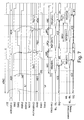
Fig. 7 shows another operation of the pseudo SRAM according to the first
embodiment. Detailed description will be omitted of the same operations as in Fig. 6.
In this example, two read operations RD are performed in succession, and the
refresh request signal REFI0Z occurs after the supply of the first read command.
The arbiter ARB of the refresh control circuit 14 shown in Fig. 2 holds the refresh
request signal REFI0Z temporarily, and outputs the refresh request signal REFI0Z as the
refresh request signal REFIZ after the output of the read/write control signal RWIZ (Fig. 7(a)).
The arbiter ARB delays the output of the refresh request signal REFIZ, thereby precluding the
output of the refresh signal REFSZ from the second refresh generator 38. Since the refresh
signal REFSZ is not output, no short refresh operation REFf is performed before the read
operation. In this way, the output of the refresh signal REFSZ is masked when no conflict
occurs between the access request and the refresh request. The short refresh operation
REFf can thus be performed only when needed. As a result, it is possible to reduce the
power consumption during operation.
Subsequently, as in Fig. 6, the first word timing signal TWX1 is output in
synchronization with the rising edge of the read/write control signal RWZ (Fig. 7(b)), the
word timing signal TWZ is output (Fig. 7(c)), and the read operation RD is performed. The
timing after the read operation RD is the same as in Fig. 6. As in Fig. 6, the chip enable
access time tCE in the read operation RD is reduced by time T1 as compared to heretofore.
Fig. 8 shows another operation of the pseudo SRAM according to the first
embodiment. Detailed description will be omitted of the same operations as in Fig. 6.
In this example, a read operation RD and a write operation WR are performed in
succession, and the read command and the refresh request signal REFI0Z occur almost at
the same time. The timing shown in Fig. 8 is the same as in Fig. 6 except that the read
operation RD corresponding to the address AD2 of Fig. 6 is replaced with the write
operation WR. That is, even when read operations RD and write operations WR are
performed repeatedly, the cycle time can be reduced as in Fig. 6.
As above, according to the present embodiment, the output of the refresh signal
REFSZ is stopped to interrupt the short refresh operation REFf when a conflict occurs
between an access request and the refresh request. The access operation corresponding to
the access request can thus be started earlier. That is, it is possible to reduce the access
time.
A normal refresh operation REF is always performed after a short refresh operation
REFf. Thus, even if the short refresh operation REFf only rewrites the memory cells MC
insufficiently, sufficient signal quantities of data are rewritten to the memory cells MC by the
subsequent refresh operation REF. Consequently, even if a conflict occurs between the
access request and the refresh request and precedence is given to the access request, it is
possible to retain the data in the memory cells MC with reliability. In particular, in the
present embodiment, the access operation can be started even earlier because the
execution time of the short refresh operation REFf is minimized.
Since the external address signal ADD (PAD) and the refresh address signal REFAD
are switched by the refresh signals REFSZ and REFZ, the switch circuit 22 can be configured
simply.
The execution times of the short refresh operation REFf and the normal refresh
operation REF are adjusted solely by changing the time of the amplifying stage AP. The
execution time of the short refresh operation REFf can thus be adjusted to a desired time
easily. In addition, since the execution times of the refresh operations REFf and REF are
adjusted by the amplifying stage AP alone, the operation control on the memory core 28 is
simplified. This allows simple circuit configuration of the core control circuit 26.
When no conflict occurs between the access request and the refresh request, the
short refresh operation REFf can be omitted to reduce the power consumption during
operation.
Since the execution time of the short refresh operation REFf to be performed before
the read operation RD and the write operations WR is set to a minimum, it is possible to
reduce the external access cycle time tERC as compared to heretofore.
Since the execution time of the normal refresh operation REF is the same as the
execution times of the read operation RD and the write operation WR, it is possible to share
the control circuits for performing these operations. Specifically, the first timing control
circuit 30 can be shared with a reduction in the circuit scale of the pseudo SRAM.
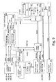
Fig. 9 shows a second embodiment of the semiconductor memory of the present
invention. The same elements as those described in the first embodiment will be
designated by identical reference numbers or symbols. Detailed description thereof will be
omitted.
In this embodiment, a core control circuit 26A is formed instead of the core control
circuit 26 of the first embodiment. The rest of the configuration is the same as in the first
embodiment. The core control circuit 26A has first and second timing control circuits 30A
and 32A, and an OR circuit 34A.
The first timing control circuit 30A outputs a first word timing signal TWX1 in
synchronization with the read/write control signal RWZ. The second timing control circuit
32A outputs a third word timing signal TWX3 and a second word timing signal TWX2 in
synchronization with the refresh signals REFZ and REFSZ, respectively. The OR circuit 34A
outputs the first, second, or third word timing signal TWX1, TWX2, or TWX3 as the word
timing signal TWZ.
Incidentally, as in the first embodiment, the core control circuit 26A has a sense
amplifier control circuit for outputting the sense amplifier activation signal LEZ and a
precharge control circuit for outputting the bit line reset signal BRS.
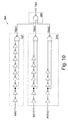
Fig. 10 shows the details of essential parts of the core control circuit 26A shown in
Fig. 9.
The first timing control circuit 30A outputs the first word timing signal TWX1
having a predetermined pulse width (a pulse of low level) in synchronization with the rising
edge of the read/write control signal RWZ. The second timing control circuit 32A outputs
the third word timing signal TWX3 having a predetermined pulse width (a pulse of low level)
in synchronization with the rising edge of the refresh signal REFZ. The second timing
control circuit 32A also outputs the second word timing signal TWX2 having a
predetermined pulse width (a pulse of low level) in synchronization with the rising edge of
the refresh signal REFSZ. The pulse widths of the timing signals TWX1-3 are set in
accordance with the numbers of stages of the inverter rows connected to the NAND gates.
That is, in this embodiment, the descending order of the selection periods of the word lines
WL is: the read operation RD and the write operation WR; the normal refresh operation REF;
and the short refresh operation REFf. The OR circuit 34A outputs the timing signals TWX1,
TWX2, and TWX3 as the word timing signal TWZ.
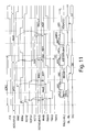
Fig. 11 shows the operation of the pseudo SRAM according to the second
embodiment. Detailed description will be omitted of the same operations as in the first
embodiment (Fig. 6).
In this example, as in Fig. 6 of the first embodiment, two read operations RD are
performed in succession and the first read command and the refresh request signal REFI0Z
occur almost at the same time. The timing of the short refresh operation REFf and the first
and second read operations RD is the same as in the first embodiment.
After the first read operation RD, the first refresh generator 36 of the refresh
control circuit 14 (Fig. 2) detects the low level of the read/write control signals RWZ and
RWIZ, and outputs the refresh signal REFZ (Fig. 11(a)). In response to the refresh signal
REFZ of high level, the switch circuit 22 outputs the same refresh address RAZ (RA1) as
when performing the short refresh operation REFf, as the row address signal IRAD (Fig.
11(b)).
The second timing control circuit 32A shown in Fig. 10 outputs the third word
timing signal TWX3 in synchronization with the refresh signal REFZ (Fig. 11(c)). The pulse
width of the third word timing signal TWX3 is smaller than that of the first word timing
signal TWX1. The timing thereof corresponds to the basic timing C shown in Fig. 5. Due
to the output of the third word timing signal TWX3, the word timing signal TWZ is output
(Fig. 11(d)), and the real refresh operation REFr corresponding to the basic timing C is
performed.
The real refresh operation REFr is performed in a cycle time tRCr which is shorter
than the cycle time tRC of the first embodiment. Consequently, there arises a margin time
tMRG in the period from the completion of the real refresh operation REFr to the start of the
second read operation RD. The margin time tMRG allows an improvement to the operation
margin of the internal circuits of the pseudo SRAM such as the core control circuit 26A. In
other words, the timing design of the pseudo SRAM is facilitated.
Fig. 12 shows another operation of the pseudo SRAM according to the second
embodiment. Detailed description will be omitted of the same operations as in Figs. 6, 7,
and 11 seen above.
In this example, two read operations RD are performed in succession, and the
refresh request signal REFI0Z occurs after the supply of the first read command. The
operations are the same as in the first embodiment (Fig. 7) except that the real refresh
operation REFr is performed between the read operations RD.
As above, the second embodiment can provide the same effects as those of the
first embodiment described above. Moreover, in this embodiment, the execution time of
the normal refresh operation REF is shorter than the execution times of the write operation
WR and the read operation RD. This produces a timing margin between the execution of
the normal refresh operation and the execution of the next access operation RD or WR.
Consequently, the core control circuit 26A and the like can be improved in operation margin,
whereby the timing design of these circuits is facilitated.
Fig. 13 shows a third embodiment of the semiconductor memory of the present
invention. The same elements as those described in the first embodiment will be
designated by identical reference numbers or symbols. Detailed description thereof will be
omitted.
In this embodiment, a refresh control part 14B, a switch circuit 22B, and a core
control circuit 26B are formed instead of the refresh control part 14, the switch circuit 22,
and the core control circuit 26 of the first embodiment. The rest of the configuration is the
same as in the first embodiment.
The refresh control circuit 14B outputs the refresh signal REFZ (high level) in
response to the read/write control signal RWIZ and the refresh request signal REFI0Z. The
switch circuit 22B outputs the refresh address signal REFAD as the internal row address
signal IRAD when the refresh signal REFZ is at high level. The switch circuit 22B outputs
the row address signal RAD as the row address signal IRAD when the refresh signal REFZ is
at low level. As will be described, the refresh signal REFZ is output not only in the normal
refresh operation REF but also in the short refresh operation REFf.
The core control circuit 26B has first and second timing control circuits 30B and
32B, and an OR circuit 34. The first timing control circuit 30B outputs a first word timing
signal TWX1 in synchronization with the read/write control signal RWZ. The second timing
control circuit 32B outputs a second word timing signal TWX2 in synchronization with the
refresh signal REFZ. The OR circuit 34 outputs the first or second word timing signal TWX1
or TWX2 as the word timing signal TWZ.
Fig. 14 shows the details of the refresh control circuit 14B shown in Fig. 13.
The refresh control circuit 14B has a refresh generator 40 for generating the
refresh signals REFZ and REFIX, and the same arbiter ARB as that of the first embodiment.
When the refresh request signal REFIZ is at high level, the refresh generator 40
changes the refresh signal REFZ to low level a first predetermined time after the rising edge
of the read/write control signal RWIZ. The refresh generator 40 changes the refresh signal
REFZ to high level a second predetermined time after the falling edge of the read/write
control signal RWIZ. The first predetermined time is shorter than the second
predetermined time. The first and second predetermined times are set by a delay circuit
DLY1. For example, the delay circuit DLY1 is constituted by connecting an even number of
inverters in series.
The refresh generator 40 also outputs a refresh count signal REFCZ when the pulse
width of the refresh signal REFZ (a pulse of high level) is greater than or equal to a
predetermined time. The refresh count signal REFCZ is fed back to the refresh timer 12.
Fig. 1 5 shows the details of essential parts of the core control circuit 26B shown in
Fig. 13.
The first timing control circuit 30B outputs the first word timing signal TWX1
having a predetermined pulse width (a pulse of low level) in synchronization with the rising
edge of the read/write control signal RWZ. The second timing control circuit 32B outputs
the second word timing signal TWX2 having a predetermined pulse width (a pulse of low
level) in synchronization with the rising edge of the refresh signal REFZ.
The pulse widths of the timing signals TWX1 and TWX2 are set in accordance with
the numbers of stages of the inverter rows connected to the NAND gates. Here, the pulse
width of the timing signal TWX2 coincides with the pulse width of the refresh signal REFZ
when the refresh signal REFZ changes to low level in synchronization with the rising edge of
the read/write control signal RWIZ (in a short refresh operation REFf). The OR circuit 34
outputs the timing signals TWX1 and TWX2 as the word timing signal TWZ.
In this embodiment, as in the first embodiment, the selection period of the word
lines WL is unchanged in a read operation RD, a write operation WR, and a normal refresh
operation, and is shorter in a short refresh operation REFf.
Fig. 16 shows the operation of the pseudo SRAM according to the third
embodiment. Detailed description will be omitted of the same operations as in the first
embodiment (Fig. 6).
In this example, as in Fig. 6 of the first embodiment, two read operations RD are
performed in succession, and the first read command and the refresh request signal REFIOZ
occur almost at the same time. The timing of the short refresh operation REFf and the first
and second read operations RD is the same as in the first embodiment. A difference lies in
the circuit operation alone.
Initially, the refresh generator 40 of the refresh control circuit 14B shown in Fig. 14
changes the refresh signal REFZ to high level in synchronization with the rising edge of the
refresh request signal REFIZ (Fig. 16(a)). In response to the refresh signal REFZ of high level,
the switch circuit 22B outputs the refresh address signal RAZ (RA1) as the row address
signal IRAD (Fig. 16(b)). The second timing control circuit 32B outputs the second word
timing signal TWX2 in synchronization with the refresh signal REFZ (Fig. 16(c)).
In response to the supply of the read command, the read/write control signal RWIZ
changes to high level (Fig. 16(d)). The refresh generator 40 changes the refresh signal
REFZ to low level the first predetermined time after the rising edge of the read/write control
signal RWIZ (Fig. 16(e)). In response to the change of the refresh signal REFZ to low level,
the second timing control circuit 32B changes the second word timing signal TWX2 to high
level (Fig. 16(f)). That is, the second word timing signal TWX2 having a pulse width
corresponding to the short refresh operation REFf is generated.
The OR circuit 34 inverts the logical level of the second word timing signal TWX2,
and outputs it as the word timing signal TWZ (Fig. 16(g)). Then, the short refresh operation
REFf is performed. In response to the change of the refresh signal REFSZ to low level, the
switch circuit 22B outputs the external address signal ADD (AD1) corresponding to the first
read command as the row address signal IRAD (Fig. 16(h)).
Subsequently, the first read operation RD is performed as in the first embodiment
(Fig. 6).
Next, the refresh generator 40 changes the refresh signal REFZ to high level the
second predetermined time after the falling edge of the read/write control signal RWIZ that
is generated in response to the first read command (Fig. 16(i)). Then, as in the first
embodiment (Fig. 6), a normal refresh operation REF is started (Fig. 16(j)).
When the high level period of the refresh signal REFZ exceeds the predetermined
period, the refresh generator 40 changes the refresh count signal REFCZ to high level in
response (Fig. 16(k)). The refresh count signal REFCZ is fed back to the refresh timer 12.
In response to the change of the refresh request signal REFI0Z (REFIZ) to low level,
the refresh generator 40 changes the refresh request signal REFIX to high level (Fig. 16(l)).
The refresh counter 16 counts up to increment the refresh address signal RAZ by "1" a
predetermined time after the rising edge of the refresh request signal REFIX (Fig. 16(m)).
The refresh generator 40 changes the refresh signal REFZ to low level the first
predetermined time after the rising edge of the read/write control signal RWIZ that is
generated in response to the second read command (Fig. 16(n)). Then, the normal refresh
operation REF is completed. In response to the change of the refresh signal REFZ to low
level, the switch circuit 22B outputs the external address signal ADD (AD2) corresponding to
the second read command as the row address signal IRAD (Fig. 16(o)).
Subsequently, the second read operation RD is performed as in the first
embodiment (Fig. 6).
Fig. 17 shows another operation of the pseudo SRAM according to the third
embodiment. Detailed description will be omitted of the same operations as in Figs. 6 and
7 seen above.
In this example, as in the first embodiment (Fig. 7), two read operations RD are
performed in succession, and the refresh request signal REFI0Z occurs after the supply of
the first read command. Thus, the short refresh operation REF will not be performed. The
late occurrence of the refresh request signal REFI0Z also delays the rising edge of the
refresh request signal REFIX (Fig. 17(a)). Consequently, the refresh counter 16 counts up
after the second read operation RD (Fig. 17(b)). The rest of the operations are the same as
in Fig. 16 seen above.
The third embodiment can provide the same effects as those of the first
embodiment described above.
Fig. 18 shows a fourth embodiment of the semiconductor memory of the present
invention. The double square in the diagram represents a test pad. The test pad is not
connected to any of the external terminals (lead frame etc.) of the product to be shipped.
For example, the test pad is connected with a prober in a probing test, and receives test
patterns. This semiconductor memory is formed as a pseudo SRAM which has DRAM
memory cells (dynamic memory cells) and an SRAM interface. The pseudo SRAM performs
periodic refresh operations inside the chip without receiving refresh commands from
exterior, thereby retaining data written in its memory cells. This pseudo SRAM is used, for
example, as a work memory to be mounted on a cellular phone.
The pseudo SRAM has an access timing generator 110, a command decoder 112, a
refresh selection circuit 114, a refresh timer 116, a refresh counter 118, an address input
circuit 120, a switch circuit 122, a data output circuit 124, a data input circuit 126, an
arbiter 128, a refresh decision circuit 130, a row operation control circuit 132, a core
control circuit 134, and a memory core 136.
The access timing generator 110 receives command signals CMD (including a chip
enable signal /CE, an output enable signal /OE, and a write enable signal /WE) from exterior
through a command terminal CMD, and outputs an access timing signal ATDPZ and the like
for performing a read operation or a write operation.
The command decoder 112 decodes the command signals CMD, and outputs a
read control signal RDZ for performing a read operation or a write control signal WRZ for
performing a write operation.
The refresh selection circuit 114 outputs an internal refresh request IREFZ, which is
output from the refresh timer 116, as a refresh timing signal SRTPZ in a normal operation
mode. The refresh selection circuit 114 outputs a test refresh signal EREFZ, which is
supplied from exterior of the pseudo SRAM through an external testing probe SRC, as the
refresh timing signal SRTPZ in test modes. That is, in the test modes, the internal refresh
request signal IREFZ output from the refresh timer 116 is masked. Instead of the internal
refresh request signal IREFZ, the test refresh request signal EREFZ is output as the refresh
timing signal SRTPZ.
Incidentally, the pseudo SRAM shifts from the normal operation mode to a test
mode (first test mode or second test mode) when it receives a plurality of command signals
CMD in a combination that is unused in normal operations. The state of the pseudo SRAM
is set to the first test mode or the second test mode in accordance with the logical values of
the command signals CMD. The pseudo SRAM maintains a test signal TES1Z at high level
when in the first test mode, and maintains a test signal TES2Z at high level when in the
second test mode.
The refresh timer 116 outputs the internal refresh request signal IREFZ at
predetermined cycles. The internal refresh request signal IREFZ is generated at cycles such
that memory cells MC can be refreshed in succession without losing the data retained in the
memory cells MC. For example, the cycle of generation of the internal refresh request
signal IREFZ is set so that all the memory cells MC are refreshed once within 300 ms. More
specifically, when there are arranged 8k word lines WL to be selected in succession by
respective refresh requests, the internal refresh request signal IREFZ is generated at every
36 to 37 µs. The refresh timer 116 is composed of, for example, a ring oscillator having an
oscillation cycle of 1 µs and a frequency divider for generating the internal refresh request
signal IREFZ from the output of the ring oscillator.
The refresh counter 118 makes a count operation in response to the internal
refresh request signal IREFZ, thereby generating a refresh address signal REFAD
successively.
The address input circuit 120 receives an address signal ADD through an address
terminal ADD, and outputs the received signal as a row address signal RAD (upper address)
and a column address signal CAD (lower address). Note that the pseudo SRAM is a memory
of address non-multiplex type which receives the upper address and the lower address
simultaneously.
The switch circuit 122 outputs the refresh address signal REFAD as an internal row
address signal IRAD when a refresh operation is performed. The switch circuit 122 outputs
the row address signal RAD as the internal row address signal IRAD when a read operation
or a write operation is performed.
The data output circuit 124 receives read data from the memory cells MC through a
common data bus CDB, and outputs the received data to data terminals DQ (DQ0-7).
Moreover, in the test modes, the data output circuit 124 sets the data terminals DQ0-7 to a
high impedance state when the data output circuit 124 receives a short refresh detection
signal REFSSZ (detecting signal) output from the refresh decision circuit 128.
The data input circuit 126 receives write data through the data terminals DQ
(DQO-7), and outputs the received data to the common data bus CDB.
The arbiter 128 compares the transition edges of the access timing signal ATDPZ
(access request) and the refresh timing signal SRTPZ (refresh request) to make a
determination on the conflict between these requests, and decides which to give precedence
to, an access operation or a refresh operation. When the access operation has precedence,
the arbiter 128 holds the refresh timing signal SRTPZ temporarily, and outputs a read timing
signal RDPZ or a write timing signal WRPZ in response to the read control signal RDZ or the
write control signal WRZ. Subsequently, the arbiter 128 detects the completion of the
access operation from the inactivation of a core cycle state signal ICSX (a change to high
level), and outputs a refresh start signal REFPZ and a refresh state signal REFIZ (second
refresh control signal) in accordance with the held refresh timing signal SRTPZ. The refresh
state signal REF1Z is a signal for indicating that a refresh operation is in execution.
When the refresh operation has precedence, the arbiter 128 holds the access timing
signal ATDPZ temporarily, and outputs the refresh start signal REFPZ and the refresh state
signal REFIZ (first refresh control signal) in response to the refresh timing signal SRTPZ.
Subsequently, the arbiter 128 detects the completion of the refresh operation from the
inactivation of the core cycle state signal ICSX (a change to high level), and outputs the read
timing signal RDPZ or the write timing signal WRPZ in accordance with the held access
timing signal ATDPZ.
Incidentally, when a short refresh signal REFS2Z is output from the refresh decision
circuit 130, the arbiter 128 outputs the refresh start signal REFPZ and the refresh state
signal REF1Z, and holds the refresh timing signal SRTPZ temporarily even after the refresh
operation is performed. Then, it detects the completion of the access operation from the
inactivation of the core cycle state signal ICSX, before outputting the refresh start signal
REFPZ and the refresh state signal REF1Z (second refresh control signal) again to perform a
refresh operation. That is, when the short refresh signal REFS2Z is output, two refresh
operations are performed in response to a single refresh request.
When the short refresh signal REFS2Z is output, the arbiter 128 outputs the refresh
state signal REF1Z (first refresh control signal) corresponding to the first refresh operation
for a period shorter than in a normal refresh operation (corresponding to a first period to be
described later). The arbiter 128 outputs the refresh state signal REF1Z (second refresh
control signal) corresponding to the second refresh operation for the same period same as
in a normal refresh operation (corresponding to a second period to be described later).
The refresh decision circuit 130 outputs the short refresh signal REFS2Z when the
interval between the transition edges of the access timing signal ATDPZ and the refresh
state signal REF1Z is shorter than a predetermined period. Besides, when in the first test
mode (TES1Z = high level), the refresh decision circuit 130 outputs the short refresh signal
REFS2Z as the short refresh detection signal REFSSZ (detecting signal). When in the second
test mode (TES2Z = high level), the refresh decision circuit 130 outputs the short refresh
detection signal REFSSZ when the short refresh signal REFS2Z is output twice in succession.
The access timing generator 110, the command decoder 112, and the arbiter 128
operate as a command control circuit. The command control circuit outputs an access
control circuit (the read timing signal RDPZ or the write timing signal WRPZ) for accessing
the memory cells MC to be described later in response to an access control signal (a read
command or a write command) supplied through the command terminal CMD.
The arbiter 128 and the refresh decision circuit 130 operate as a refresh control
circuit. The refresh control circuit outputs the first refresh control signal (REF1Z) for
activating sense amplifiers for the first period or the second refresh control signal (REF1Z)
for activating the sense amplifiers for the second period longer than the first period in
accordance with the timing of occurrence of the access request and the internal refresh
request.
The row operation control circuit 132 outputs a row control signal RASZ, or a basic
timing signal for operating the memory core 136, when it receives the read timing signal
RDPZ, the write timing signal WRPZ, or the refresh timing signal SRTPZ. It also maintains
the core cycle state signal ICSX at low level when the memory core 136 is in operation.
Incidentally, the row operation control circuit 132 performs a normal refresh operation
(second refresh operation) when it receives the refresh timing signal SRTPZ without
receiving the short refresh signal REFS2Z. It performs a short refresh operation (first
refresh operation) shorter than the normal refresh operation when it receives the short
refresh signal REFS2Z and the refresh timing signal SRTPZ as well.
The core control circuit 134 has a word line control circuit, a sense amplifier control
circuit, and a precharge control circuit which are not shown. The word line control circuit
outputs a word line control signal TWZ for selecting word lines WL to be described later, in
response to the rpw control signal RASZ. The sense amplifier control circuit outputs a
sense amplifier activation signal LEZ for activating the sense amplifiers of a sense amplifier
part SA to be described later, in response to the row control signal RASZ. The precharge
control circuit outputs a bit line reset signal BRS when bit lines BL and /BL are not in use.
The row operation control circuit 132 and the core control circuit 134 operate as an
operation control circuit. The operation control circuit makes the memory core 136
perform an access operation in response to the read timing signal RDPZ (access control
signal) or the write timing signal WRPZ (access control signal), and makes the memory core
136 perform first and second refresh operations in response to first and second refresh
control signals REFIZ.
The memory core 136 has a memory cell array ARY, a word decoder part WDEC, the
sense amplifier part SA, a column decoder part CDEC, a sense buffer part SB, and a write
amplifier part WA. The memory cell array ARY has a plurality of volatile memory cells MC
(dynamic memory cells), and a plurality of word lines WL and a plurality of bit lines BL and
/BL (complementary bit lines) which are connected to the memory cells MC. The memory
cells MC are the same as typical DRAM memory cells, each having a capacitor for retaining
data in the form of a charge and a transfer transistor arranged between this capacitor and a
bit line BL (or /BL). The gate of the transfer transistor is connected to a word line WL.
Through the selection of the word lines WL, any one of a read operation, a write operation,
and a refresh operation is performed. The memory cell array ARY performs any one of the
read operation, write operation, and refresh operation before performing a precharge
operation for precharging the bit lines BL and /BL to a predetermined voltage in response to
the bit line reset signal BRS.
When the word decoder part WDEC receives the word line control signal TWZ of
high level, it selects any one of the word lines WL in accordance with the internal row
address signal IRAD, and changes the selected word line WL to high level. The column
decoder part CDEC outputs a column line signal for turning on column switches which
connect the bit lines BL and /BL and a data bus DB, respectively, in accordance with the
column address signal CAD.
The sense amplifier part SA has a plurality of sense amplifiers. The sense
amplifiers operate in response to the sense amplifier activation signal LEZ, and amplify data
on the respective bit lines BL and /BL in signal quantity. The data amplified by the sense
amplifiers is transmitted to the data bus DB through the column switches in a read
operation. In a write operation, the data is written to the memory cells MC through the bit
lines.
The sense buffer part SB amplifies the read data on the data bus DB in signal
quantity, and outputs it to the common data bus CDB. The write amplifier part WA
amplifies the write data on the common data bus CDB in signal quantity, and outputs it to
the data bus DB.
Fig. 19 shows the details of the refresh decision circuit 130 shown in Fig. 18.
The refresh decision circuit 130 has a compared signal generator 138, a short
refresh decision circuit 140, a short refresh latch circuit 142, and a selector circuit 144.
The compared signal generator 138 generates a compared signal ATDREFZ in
accordance with the access timing signal ATDPZ. The short refresh decision circuit 140
compares the transition edge of the refresh state signal REF1Z and the transition edge of
the compared signal ATDREFZ, and decides which refresh operation for the refresh state
signal REF1Z to indicate, a normal refresh operation or a short refresh operation. When the
short refresh decision circuit 140 decides to perform a short refresh operation, it outputs
the short refresh signal REFS2Z.
The short refresh latch circuit 142 latches the logical level of the short refresh
signal REFS2Z in synchronization with the falling edge of the refresh state signal REF1Z, and
outputs the latched logical level as a short refresh signal REFSCZ. Consequently, the short
refresh signal REFSCZ changes to high level when a short refresh operation is performed,
and changes to low level when a normal refresh operation is performed. In addition, the
short refresh latch circuit 142 is reset during the high level period of a reset signal RESET2Z,
and changes the short refresh detection signal REFSSZ to low level. The reset signal
RESET2Z changes to high level for a predetermined period when a reset command is
received as a command signal CMD in the second test mode.
The selector circuit 144 outputs the short refresh signal REFS2Z as the short refresh
detection signal REFSSZ when the test signal TES1Z is at high level (the first test mode).
The selector circuit 144 outputs the AND logic of the short refresh signal REFS2Z and the
short refresh signal REFSCZ as the short refresh detection signal REFSSZ when the test signal
TES2Z is at high level (the second test mode). As will be described, in the first test mode,
the short refresh detection signal REFSSZ is output each time a short refresh operation is
performed. In the second test mode, the short refresh detection signal REFSSZ is output
when two short refresh operations are performed in succession. The selector circuit 144
thus operates as a detecting circuit, which operates in the test modes and outputs the short
refresh detection signal REFSSZ when the refresh state signal REFIZ (first refresh control
signal) for performing a short refresh operation is detected.
Fig. 20 shows the details of the data output circuit 124 shown in Fig. 18.
The data output circuit 124 has an output mask circuit 146 and output buffer
circuits 148. Note that Fig. 20 shows an output buffer circuit 148 that corresponds to the
data terminal DQ0. The output buffer circuits corresponding to the other data terminals
DQ1-7 are identical to the output buffer circuit 148. The output mask circuit 146 is
common among the output buffer circuits 148 corresponding to the data terminals DQ0-7.
The output mask circuit 146 is reset by a reset signal RESET1Z of high level, and
inverts and outputs a read timing signal READZ as an output enable signal ODEX. The
output mask circuit 146 prohibits the output of the read timing signal READZ when it
receives the short refresh detection signal REFSSZ of high level. That is, the output enable
signal ODEX is kept at high level by the short refresh detection signal REFSSZ of high level.
When the output enable signal ODEX is at low level, the output buffer circuit 148
operates its tristate output buffer 148a in accordance with the logic level of read data
DATA0X, thereby outputting a high level or low level to the data terminal DQ0. When the
output enable signal ODEX is at high level, the output buffer circuit 148 changes the output
of the tristate output buffer 148a to a high impedance state. That is, the output mask
circuit 146 controls the tristate output buffer 148a in the test mode so that the output of
the read data DATA0X to the data terminal DQ0 is prohibited in response to the short
refresh detection signal REFSSZ and the data terminal DQ0 is set to a high impedance state.
Fig. 21 shows the basic operations of the memory cell array ARY according to the
fourth embodiment.
In this embodiment, a write operation WR, a read operation RD, and a normal
refresh operation REF (second refresh operation) are performed in the same cycle time tRC.
A short refresh operation REFf (first refresh operation) is performed in a cycle time tRCf
shorter than the cycle time tRC. The write operation WR, the read operation RD, the normal
refresh operation REF, and the short refresh operation REFf consist of a read stage RP, an
amplifying stage AP1 or AP2, and a precharging stage PP.
The read stage RP is a period in which data is read to the bit lines BL (or /BL) from
memory cells MC that are selected in response to the activation (selection) of a word line WL.
The amplifying stages AP1 and AP2 are periods in which, after the data is read to the bit
lines BL (or /BL), the sense amplifiers are activated in response to the sense amplifier
activation signal LEZ to amplify the voltage differences (data) between the bit lines BL and
/BL, and the amplified voltages of the bit lines BL and /BL are rewritten to the memory cells
MC from which the data is read. The period of the amplifying stage AP2 (the high level
period of the sense amplifier activation signal LEZ in the normal refresh operation REF)
corresponds to the second period. The amplifying stage AP1 (the high level period of the
sense amplifier activation signal LEZ during the short refresh operation REFf) corresponds to
the first period. The precharging stage PP is a period in which the word lines WL are
inactivated (deselected) and the bit lines BL and /BL are precharged to a predetermined
voltage.
In the write operation WR, the data that is read from the memory cells MC and
amplified on the bit lines BL and /BL must be inverted by write data. This makes the cycle
time of the write operation WR longer than those of the other operations. In this
embodiment, however, the cycle time of the read operation RD is set to the same value as
the cycle time of the write operation WR in view of user convenience.
Moreover, in the normal refresh operation REF, the bit lines BL and /BL need not be
connected with the data bus DB, nor need the data be inverted on the bit lines BL and /BL.
Thus, the data retained in the memory cells MC can be fully written to the memory cells MC
again even if the cycle time is shorter than tRC. The full write gives each memory cell MC a
data retention time (pause time) of 64 ms or more. In this embodiment, however, the cycle
time of the normal refresh operation REF is set to the same value as the cycle time of the
write operation WR in order to simplify the configuration of the row operation control circuit
132 and the core control circuit 134.
The short refresh operation REFf is used to perform a refresh operation for a
minimum period when a conflict occurs between an access request (the read command or
the write command) and a refresh request. After the short refresh operation REFf, the
access operation (the read operation RD or the write operation WR) can be performed
immediately to reduce the access time.
The short refresh operation REFf will not amplify the voltage differences between
the bit lines BL and /BL sufficiently because the activation period of the sense amplifiers (the
high level period of the LEZ signal) is short. Since the data rewritten to the memory cells
MC is small in signal quantity (restore level), a normal refresh operation REF must be
performed within, e.g., 200 ns after the short refresh operation REFf. In other words, when
it is possible to perform a normal refresh operation REF within 200 ns, the short refresh
operation REFf can be temporarily performed to avoid loss of data in the memory cells MC.
As above, the execution time of the short refresh operation REFf (the time for amplifying
and rewriting data) is such a time that the data in the memory cells MC can be retained
without loss over the period from the execution of the short refresh operation REFf to the
execution of the normal refresh operation REF.
Fig. 22 shows an example of operation of the fourth embodiment in the normal
operation mode.
In this example, two read operations RD are performed in succession, and the first
read command RD and the internal refresh request signal IREFZ occur almost at the same
time.
Initially, the access timing generator 110 shown in Fig. 18 receives the chip enable
signal /CE of low level and the not-shown output enable signal /OE of low level, and
outputs the access timing signal ATDPZ (Fig. 22(a)). The command decoder 112 receives
the chip enable signal /CE of low level, and the output enable signal /OE of low level and the
write enable signal /WE of high level which are not shown, and detects that a read command
RD (read access request) is supplied. The command decoder 112 outputs the read control
signal RDZ (Fig. 22(b)).
The refresh timer 116 shown in Fig. 19 outputs the internal refresh request signal
IREFZ almost at the same time as the supply of the read command RD. The refresh
selection circuit 114 outputs the refresh timing signal SRTPZ in response to the internal
refresh request signal IREFZ (Fig. 22(c)).
The arbiter 128 decides to perform the refresh operation with precedence over the
read operation, and outputs the refresh start signal REFPZ and the refresh state signal REF1Z
(first refresh control signal) in succession (Fig. 22(d)). The refresh decision circuit 130
detects that the access timing signal ATDPZ is generated a predetermined time earlier than
the refresh state signal REF1Z, and outputs the short refresh signal REFS2Z (Fig. 22(e)). The
switch circuit 122 outputs the refresh address signal REFAD (RA1) as the row address signal
IRAD (Fig. 22(f)) in order to perform a short refresh.
The row operation control circuit 132 outputs the row control signal RASZ in
synchronization with the refresh start signal REFPZ (Fig. 22(g)). The core control circuit 134
outputs the word line control signal TWZ and the like in response to the row control signal
RASZ. Then, the short refresh operation REFf (first refresh operation) shown in Fig. 21 is
performed (Fig. 22(h)). The row operation control circuit 132 changes the core cycle state
signal ICSX to low level while the short refresh operation REFf is in execution (Fig. 22(i)).
After the execution of the short refresh operation REFf, the arbiter 128 changes the
refresh state signal REF1Z to low level (Fig. 22(j)). The switch circuit 122 outputs the
address signal ADD (AD1) as the row address signal IRAD (Fig. 22(k)) in order to perform a
read operation.
The arbiter 128 outputs the read timing signal RDPZ in response to the rising edge
of the core cycle state signal ICSX (Fig. 22(l)). The row operation control circuit 132
outputs the row control signal RASZ in synchronization with the read timing signal RDPZ (Fig.
22(m)). The core control circuit 134 outputs the word line control signal TWZ and the like
in response to the row control signal RASZ. Then, the read operation RD shown in Fig. 21
is performed (Fig. 22(n)). The read data D0 that is amplified on the bit lines BL and /BL by
the read operation RD is output to the data terminals DQ through the common data bus
CDB (Fig. 22(o)).
The short refresh operation REFf ends in a short period as shown in Fig. 21. Thus,
even when a conflict occurs between a refresh request and an access request and
precedence is given to the refresh request, the access operation corresponding to the
access request can be started earlier. That is, it is possible to reduce the chip enable
access time from the falling edge of the chip enable signal /CE to the output of data to the
data terminals DQ.
Next, the arbiter 128 outputs the refresh start signal REFPZ and the refresh state
signal REF1Z (second refresh control signal) in succession in response to the rising edge of
the core cycle state signal ICSX (Fig. 22(p)). Since the generation of the access timing
signal ATDPZ cannot be detected, the refresh decision circuit 130 will not output the short
refresh signal REFS2Z (Fig. 22(q)). The switch circuit 22 outputs the refresh address signal
REFAD (RA1) as the row address signal IRAD (Fig. 22(r)) in order to perform a normal refresh
after the short refresh operation.
The row operation control circuit 132 outputs the row control signal RASZ in
synchronization with the refresh start signal REFPZ (Fig. 22(s)). The core control circuit 134
outputs the word line control signal TWZ and the like in response to the row control signal
RASZ. Then, the normal refresh operation REFf (second refresh operation) shown in Fig. 21
is performed (Fig. 22(t)). The refresh operation corresponding to the second refresh
control signal is always performed after the refresh operation corresponding to the first
refresh control signal (the first refresh operation). Thus, even if the first refresh operation
only rewrites the memory cells insufficiently, sufficient signal quantities of data are rewritten
to the memory cells by the subsequent refresh operation. Consequently, even when a
conflict occurs between an access request and the refresh request and precedence is given
to the access request, it is possible to retain the data in the memory cells with reliability.
The pseudo SRAM receives a read command (the chip enable signal /CE of low level,
and the output enable signal /OE of low level and the write enable signal /WE of high level
which are not shown) while the refresh operation REF is in execution (Fig. 22(u)). The
access timing generator 110 and the command decoder 112 output the access timing signal
ATDPZ and the read control signal RDZ in response to the read command (Fig. 22(v)).
The arbiter 128 outputs the read timing signal RDPZ in response to the rising edge
of the core cycle state signal ICSX of the normal refresh operation REF (Fig. 22(w)). The row
operation control circuit 132 outputs the row control signal RASZ in synchronization with
the read timing signal RDPZ (Fig. 22(x)). The core control circuit 134 outputs the word line
control signal TWZ and the like in response to the row control signal RASZ. Then, the read
operation RD corresponding to the address signal AD2 is performed (Fig. 22(y)). The read
data D1 that is amplified on the bit lines BL and /BL by the read operation RD is output to
the data terminals DQ through the common data bus CDB (Fig. 22(z)).
As shown in Fig. 22, when the internal refresh request signal IREFZ has precedence
over the read command RD (access request), the arbiter 128 outputs the refresh state signal
REF1Z (first refresh control signal), the read timing signal RDPZ, and the refresh state signal
REF1Z (second refresh control signal) in succession.
Incidentally, this pseudo SRAM is designed so that the sum of the execution times
of the short refresh operation REFf and the normal refresh operation REF and the execution
times of two read operations RD is smaller than twice the minimum interval of supply of
access requests, or the external access cycle time. Consequently, the short refresh
operation REFf, the normal refresh operation REF, and the two read operations RD (or write
operations) can be performed during the two external access cycle times. That is, the
pseudo SRAM can perform refresh operations without being recognized from exterior.
Fig. 23 shows another example of operation of the fourth embodiment in the
normal operation mode. Detailed description will be omitted of the same operations as in
Fig. 22.
In this example, a write operation WR and a read operation RD are performed in
succession, and the write command and the internal refresh request signal IREFZ occur
almost at the same time.
The refresh timer 116 outputs the internal refresh request signal IREFZ almost at
the same time as the supply of the write command WR (Fig. 23(a)). The arbiter 128 decides
to perform the refresh operation with precedence over the write operation, and outputs the
refresh start signal REFPZ and the refresh state signal REF1Z (first refresh control signal) in
succession (Fig. 23(b)). The refresh decision circuit 130 detects that the access timing
signal ATDPZ is generated a predetermined time earlier than the refresh state signal REF1Z,
and outputs the short refresh signal REFS2Z (Fig. 23(c)).
Then, as in Fig. 22, the short refresh operation REFf (first refresh operation), the
write operation WR (access operation), and the normal refresh operation REF (second refresh
operation) are performed in succession (Fig. 23(d), (e), (f)). After the refresh operation is
performed, the read operation corresponding to the address signal AD2 is performed (Fig.
23(g)).
As shown in Fig. 23, when the internal refresh request signal IREFZ has precedence
over the write command WR (access request), the arbiter 28 outputs the refresh state signal
REF1Z (first refresh control signal), the write timing signal WRPZ, and the refresh state signal
REF1Z (second refresh control signal) in succession.
Fig. 24 shows another example of operation of the fourth embodiment in the
normal operation mode. Detailed description will be omitted of the same operations as in
Fig. 22.
In this example, two read operations RD are performed in succession, and the
internal refresh request signal IREFZ occurs after the supply of the first read command RD.
The arbiter 128 receives the access timing signal ATDPZ before it receives the
refresh timing signal SRTPZ. The arbiter 128 thus decides to perform the read operation
with precedence over the refresh operation. Then, the arbiter 128 outputs the read timing
signal RDPZ without outputting the refresh start signal REFPZ or the refresh state signal
REF1Z (Fig. 24(a)).
Since the refresh decision circuit 130 receives the access timing signal ATPDZ
without receiving the refresh state signal REF1Z, it will not output the short refresh signal
REFS2Z (Fig. 24(b)). In this way, no short refresh operation is performed when the read
command RD (or the write command WR) has precedence over the refresh command (the
internal refresh request signal IREFZ). After the supply of the read command RD, the
internal refresh request signal IREFZ is generated (Fig. 24(c)). Then, the read operation RD
corresponding to the address AD1 is performed with precedence over the refresh operation
(Fig. 24(d)).
The arbiter 128 outputs the refresh start signal REFPZ and the refresh state signal
REF1Z in synchronization with the rising edge of the core cycle state signal ICSX that results
from the completion of the read operation RD (Fig. 24(e)). Then, as in Fig. 22, the normal
refresh operation REF (second refresh operation) and the read operation RD corresponding
to the address AD2 are performed in succession (Fig. 24(f), (g)). As above, when the read
command RD (access request) has precedence over the internal refresh request signal IREFZ,
the arbiter 128 outputs the read timing signal RDPZ before outputting the refresh state
signal REF1Z (second refresh control signal).
Fig. 25 shows an example of operation of the fourth embodiment in the first test
mode. Detailed description will be omitted of the same operations as in Fig. 22. The
pseudo SRAM has already shifted from the normal operation mode to the first test mode.
The first test mode is used, for example, for characteristic evaluations on the pseudo SRAM
under development. The characteristic evaluations are conducted by connecting the
pseudo SRAM in a wafer state with probers and inputting test patterns to the pseudo SRAM
from the LSI tester.
This example shows the timing when the timing of supply of the test refresh
request signal EREFZ with respect to the read command RD is advanced gradually until the
timing of occurrence of the short refresh operation is found. That is, the timing at which a
conflict occurs between a refresh request and an access request is shown. The timing
immediately preceding Fig. 25 (the timing before the occurrence of the short refresh
operation) is the same as in Fig. 24 seen above.
In the first test mode, the refresh selection circuit 114 shown in Fig. 18 masks the
internal refresh request signal IREFZ output from the refresh timer 116. The refresh
selection circuit 114 receives the test refresh request signal EREFZ supplied from the LSI
tester through the testing probe SRC instead of the internal refresh request signal IREFZ,
and outputs it as the refresh timing signal SRTPZ (Fig. 25(a)). Since a refresh request and
an access request of desired timing can be supplied from exterior of the pseudo SRAM by
using the LSI tester or the like, it is possible to control the deviation (time difference)
between the access request and the refresh request with high precision.
In the first test mode, the LSI tester gradually advances, for example, the timing of
supply of the test refresh request signal EREFZ with respect to an access command (e.g.,
read command RD). Then, the timing at which precedence is given to the refresh operation
over the read operation to perform a short refresh operation is found. That is, it is possible
to detect the timing at which the short refresh operation REFf and the normal refresh
operation REF are switched.
In the first test mode, the selector circuit 144 of the refresh decision circuit 130
shown in Fig. 19 outputs the short refresh signal REFS2Z as the short refresh signal REFSSZ
in response to the test signal TES1Z of high level (Fig. 25(b)). In response to the short
refresh signal REFSSZ, the output mask circuit 146 of the data output circuit 124 shown in
Fig. 20 masks the read timing signal READZ to fix the output enable signal ODEX to high
level. This inactivates the output buffer circuits 148 of the data output circuit 124 shown
in Fig. 20. The tristate output buffers 148a prohibit the read data D0 resulting from the
read operation RD from being output to the data terminals DQ, and set the data terminals
DQ to a high impedance state Hi-Z (Fig. 25(c)). That is, in the first test mode, the data
terminals DQ enter the high impedance state Hi-Z when the short refresh operation REFf is
performed. Then, whether or not a conflict occurs between the refresh request and the
access request is decided depending on if the high impedance state Hi-Z is detected. Since
the foregoing evaluation does not require the formation of any dedicated testing probe, the
pseudo SRAM can be prevented from an increase in chip size.
In an actual evaluation, an evaluation board or probe card having its data terminals
DQ pulled up (logic "1") is loaded into the LSI tester so that logic "0" is written to the
memory cells MC corresponding to the address AD1 in advance. Then, if the logic "0"
cannot be read and an error occurs in the foregoing test, it is determined that the short
refresh operation REFf is performed due to a conflict between the refresh request and the
access request.
The data terminals DQ remain in the high impedance state Hi-Z until a reset signal
RESET1Z is supplied to the output mask circuit 146. Consequently, when the short refresh
operation REFf is performed, a read error occurs even in the read operation RD
corresponding to the address AD2 (Fig. 25(d)).
Note that Fig. 25 shows the case where the read operation RD corresponding to the
address AD1 is performed to evaluate the conflict between the read command and the
refresh request. Nevertheless, as shown in Fig. 23, a write operation WR corresponding to
the address AD1 may be performed to evaluate the conflict between the write command and
the refresh request.
After the timing of occurrence of the short refresh operation is evaluated in the first
test mode, the pseudo SRAM enters the second test mode to make another evaluation based
on the result of evaluation in the first test mode.
Figs. 26 and 27 show examples of operation of the fourth embodiment in the
second test mode. Detailed description will be omitted of the same operations as in Fig. 22.
The pseudo SRAM has already shifted from the normal operation mode or the first test
mode to the second test mode. Like the first test mode, the second test mode is used for
characteristic evaluations on the pseudo SRAM under development, for example. The
characteristic evaluations are conducted by connecting the pseudo SRAM in a wafer state
with probers and inputting test patterns to the pseudo SRAM from the LSI tester.
In the second test mode, the refresh selection circuit 1 14 shown in Fig. 18 masks
the internal refresh request signal IREFZ output from the refresh timer 116. The refresh
selection circuit 114 receives the test refresh request signal EREFZ supplied from the LSI
tester through the testing probe SRC instead of the internal refresh request signal IREFZ,
and outputs it as the refresh timing signal SRTPZ (Fig. 26(a), Fig. 27(a)).
In the second test mode, the LSI tester gradually decreases a cycle time (for
example, the read cycle time) without changing the timing condition evaluated in the first
test mode. Then, the timing at which the normal refresh operation REF to be performed
after the short refresh operation REFf switches to a short refresh operation REFf is found.
That is, an evaluation on the minimum cycle time at which the pseudo SRAM operates
properly is made.
The basic timing shown in Fig. 26 is the same as in Fig. 22. Here, the pseudo
SRAM is in proper operation, so that the short refresh operation REFf, the read operation RD,
and the normal refresh operation REF are performed in succession (Fig. 26(b), (c), (d)).
When the short refresh operation REFf is performed, the short refresh latch circuit 142 of
the refresh decision circuit 130 shown in Fig. 19 latches the short refresh signal REFS2Z of
high level in synchronization with the falling edge of the refresh state signal REF1Z, and
outputs it as the short refresh signal REFSCZ (Fig. 26(e)).
Moreover, when the normal refresh operation REF is performed after the short
refresh operation REFf, the short refresh latch circuit 142 latches the short refresh signal
REFS2Z of low level in synchronization with the falling edge of the refresh state signal REF1Z,
and outputs it as the short refresh signal REFSCZ (Fig. 26(f)). That is, the short refresh
signal REFSCZ changes from high level to low level.
As shown in Fig. 26, the high level periods of the short refresh signals REFS2Z and
REFSSZ do not overlap with each other. The short refresh signal REFSSZ thus remains at
low level (Fig. 26(g)). Consequently, the output buffer circuit 148 shown in Fig. 20 is not
inactivated by the short refresh signal REFSSZ. As a result, the read data D1 resulting from
the read operation RD is output to exterior of the pseudo SRAM through the data terminals
DQ (Fig. 26(h)). That is, if a conflict occurs between the refresh operation and the access
operation, the correct data D1 is read out when the pseudo SRAM operates properly.
In contrast, Fig. 27 shows an example where the pseudo SRAM fails to operate
properly due to an excessively short cycle time. Here, the short refresh operation REFf, the
read operation RD, and the short refresh operation REFf are performed in succession (Fig.
27(b), (c), (d)). In Fig. 27, the short refresh operation REFf is performed instead of the
normal refresh operation REF (Fig. 27(d)). Thus, the memory cells MC are not rewritten
with sufficient charges, and the data retained in the memory cells MC disappears.
In this example, the short refresh signal REFS2Z is output for the short refresh
operation REFf after the read operation RD corresponding to the address AD1 (Fig. 27(e)).
When the short refresh operation REFf is performed, the short refresh latch circuit 142
latches the short refresh signal REFS2Z of high level again in synchronization with the falling
edge of the refresh state signal REF1Z, and outputs it as the short refresh signal REFSCZ (Fig.
27(f)). The high level periods of the short refresh signals REFS2Z and REFSSZ thus overlap
with each other, and the short refresh signal REFSSZ changes to high level (Fig. 27(g)).
In response to the short refresh signal REFSSZ, the output mask circuit 146 of the
data output circuit 124 shown in Fig. 20 masks the read timing signal READZ to fix the
output enable signal ODEX to high level. This inactivates the output buffer circuits 148 of
the data output circuit 124 shown in Fig. 20. The tristate output buffers 148a prohibit the
read data D1 resulting from the read operation RD corresponding to the address signal AD2
from being output to the data terminals DQ, and set the data terminals DQ to the high
impedance state Hi-Z (Fig. 27(h)).
Consequently, as in Fig. 25, when the data terminals DQ are pulled up (logic "1"),
the output buffer circuit 148s are determined to be inactivated due to the execution of the
short refresh operation when the logic "0" previously written in the memory cells MC cannot
be read and an error occurs. That is, an evaluation on the minimum cycle time at which the
pseudo SRAM performs a proper refresh operation is made by detecting the occurrence of
the two consecutive short refresh signals REFS2Z.
Figs. 26 and 27 show the cases where the read operation RD corresponding to the
address AD1 is performed to evaluate the conflict between the read command and the
refresh request. Nevertheless, as shown in Fig. 23, the write operation WR corresponding
to the address AD1 may be performed to evaluate the conflict between the write command
and the refresh request.
Incidentally, whether or not the pseudo SRAM having a short refresh function
performs refresh operations properly can be evaluated by checking if the data written in the
memory cells MC disappears actually. To be more specific, tests for evaluating the memory
cells for data retention characteristics (typically referred to as pause tests) can be conducted
while gradually shifting the refresh request with respect to the access request. The data
written in DRAM memory cells MC, however, is retained for several hundreds of milliseconds
to several seconds. Then, checking for the proper execution of refresh operations through
pause tests can require enormous amounts of test time.
As above, in the fourth embodiment, the data terminals DQ are set to a high
impedance state when a conflict occurs between a refresh request and an access request,
and a short refresh operation REFf is performed. Thus, the evaluation apparatus for
evaluating the pseudo SRAM, such as an LSI tester, can easily and precisely evaluate the
timing at which the short refresh operation REFf is inserted. That is, the timing at which
the conflict occurs between the refresh request and the access request can be evaluated
easily. As a result, the development period of the pseudo SRAM can be reduced with a
reduction in development cost. In mass-producing the pseudo SRAM, when failures occur
from variations of the manufacturing conditions and the like, failure analyses can be
conducted promptly to allow the minimization of the low yield period.
Moreover, when short refresh operations REFf occur consecutively to cause an
operation failure, the timing of occurrence of the failure can be surely evaluated from the
detecting signal REFSSZ.
The data terminals DQ connected to the tristate output buffers 148a are used as
external testing probes in the test modes. This eliminates the need for the formation of
new terminals for evaluation, and can thus avoid an increase in the chip size of the pseudo
SRAM.
When a conflict occurs between an access request and a refresh request, a short
refresh operation REFf which ends in a short time is performed before the access operation.
Thus, even when the refresh request has precedence over the access request, the access
operation corresponding to the access request can be started earlier. That is, it is possible
to reduce the access time.
When the short refresh operation REFf is performed, a normal refresh operation REF
is always performed after the access operation. Consequently, even if a conflict occurs
between an access request and a refresh request and precedence is given to the access
request, it is possible to retain the data in the memory cells MC with reliability.
Fig. 28 shows a fifth embodiment of the semiconductor memory of the present
invention. The same elements as those described in the fourth embodiment will be
designated by identical reference numbers or symbols. Detailed description thereof will be
omitted.
In this embodiment, a command decoder 112A and a refresh timer 116A are
formed instead of the command decoder 112 and the refresh timer 116 of the fourth
embodiment. Moreover, neither the refresh selection circuit 114 nor the external testing
probe SRC is formed in this embodiment. The rest of the configuration is almost the same
as in the fourth embodiment.
The command decoder 112A decodes the command signals CMD, and outputs the
read control signal RDZ for performing a read operation or the write control signal WRZ for
performing a write operation. Moreover, in first and second test modes, the command
decoder 112A outputs a refresh adjustment signal REFADJ for changing the cycle of the
refresh timer 116A in accordance with the command signals CMD (test command) supplied
to the command terminal CMD.
The refresh timer 116A outputs the internal refresh request signal IREFZ at
predetermined cycles. In a normal operation mode, the internal refresh request signal
IREFZ is generated at cycles such that the memory cells MC can be refreshed in succession
without losing the data retained in the memory cells MC. In the first and second test
modes, the internal refresh request signal IREFZ is generated at cycles corresponding to the
logical value of the refresh adjustment signal REFADJ.
In this embodiment, the same evaluations as those of the fourth embodiment are
conducted while the cycle of the refresh timer 116A is changed by the test command which
is supplied through the command terminal CMD in the first and second test modes.
As above, the fifth embodiment can provide the same effects as those of the fourth
embodiment described above. Moreover, in this embodiment, the refresh timer 116A
receives the refresh adjustment signal REFADJ for changing the cycle of generation of
refresh requests in the first and second test modes. It is therefore possible to generate
refresh requests of desired timing inside the pseudo SRAM by using the circuits that operate
in normal operations. Consequently, it is possible to evaluate the refresh characteristics
under the same conditions as in the actual circuit operations of the pseudo SRAM.
Fig. 29 shows a sixth embodiment of the semiconductor memory of the present
invention. The same elements as those described in the foregoing first and second
embodiments will be designated by identical reference numbers or symbols. Detailed
description thereof will be omitted. The double square in the diagram represents a test
pad (external testing probe SRC). The test pad is not connected to any of the external
terminals (lead frame etc.) of the product to be shipped. For example, the test pad is
connected with a prober in a probing test, and receives test patterns. This semiconductor
memory is formed as a pseudo SRAM which has DRAM memory cells (dynamic memory
cells) and an SRAM interface.
In this embodiment, a command control circuit 10B, a refresh control circuit 14B,
and a refresh counter 16B are formed instead of the command control circuit 10, the refresh
control circuit 14, and the refresh counter 16 of the second embodiment. In addition, a
test control circuit 42 is formed newly. The rest of the configuration is almost the same as
in the second embodiment.
When the command control circuit 10B receives a plurality of command signals /CE,
/OE, and /WD in a combination that is unused in normal operations, it outputs a test mode
signal TMDZ (high level) in order to shift the pseudo SRAM from a normal operation mode to
a test mode. In the test mode, the command control circuit 10B prohibits the output of the
read/write control signals RWZ and RWIZ, the read control signal RDZ, and the write control
signal WRZ. That is, neither a read operation nor a write operation is performed in the test
mode.
The refresh control circuit 14B stops operating when it receives the test mode
signal TMDZ of high level. That is, in the test mode, the refresh control circuit 14B outputs
neither of the refresh signals REFZ and REFSZ.
When the refresh counter 16B receives the test mode signal TMDZ of high level, it
masks the input of the refresh signal REFZ, and receives the test refresh request signal
EREFZ which is supplied from exterior of the pseudo SRAM through the external testing
probe SRC.
The test control circuit 42 is activated when it receives the test mode signal TMDZ
of high level, and outputs the refresh signal REFSZ (first refresh signal) and the refresh
signal REFZ (second refresh signal) in response to the test refresh request signal EREFZ.
That is, in the test mode, refresh operations are performed by the refresh signal REFSZ (first
test refresh signal) and the refresh signal REFZ (second test refresh signal) that are output
from the test control circuit 42.
As will be described, the interval of generation of the refresh signals REFSZ and
REFZ for the test control circuit 42 to generate in the test mode corresponds to the pulse
width of the test refresh request signal EREFZ. Incidentally, the interval of generation of the
refresh signals REFSZ and REFZ in the normal refresh mode is set as in the first embodiment,
or at approximately 200 ns.
Fig. 30 shows an example of operation of the sixth embodiment in the test mode.
Initially, before a shift to the test mode, predetermined data (expected values) is
written to the memory cells MC of the pseudo SRAM. Next, a test command is supplied to
the pseudo SRAM, and the pseudo SRAM shifts from the normal operation mode to the test
mode. The command control circuit 10B maintains the test mode signal TMDZ at high level
(Fig. 30(a)).
Next, the test refresh request signal EREFZ having a pulse waveform is supplied
from the external testing probe SRC (Fig. 30(b)). The test control circuit 42 outputs the
refresh signal REFSZ for performing a short refresh operation in synchronization with the
rising edge of the test refresh request signal EREFZ (Fig. 30(c)). The test control circuit 42
also outputs the refresh signal REFZ for performing a normal refresh operation in
synchronization with the falling edge of the test refresh request signal EREFZ (Fig. 30(d)).
In this way, the pulse width of the test refresh request signal EREFZ corresponds to the
interval of generation of the refresh signals REFSZ and REFZ. In other words, the pulse
width of the test refresh request signal EREFZ corresponds to a difference DIF between the
start time of the short refresh operation and the start time of the normal refresh operation.
The refresh counter 16B counts up in synchronization with the test refresh request
signal EREFZ, and outputs the refresh address signal REFAD (RADZ) (Fig. 30(e)). Then, the
word lines WL are switched in succession in accordance with the refresh address signal
REFAD, so that a short refresh operation and a normal refresh operation are performed on
each single word line WL successively.
When the data rewritten (restored) to the memory cells MC by a short refresh
operation is retained in the memory cells MC until a normal refresh operation, the correct
data is rewritten to the memory cells MC by the refresh operation. On the other hand,
when the data rewritten to the memory cells MC by the short refresh operation is not
retained in the memory cells MC until the normal refresh operation, the data in the memory
cells MC is corrupted. Here, the incorrect data is rewritten to the memory cells MC by the
normal refresh operation.
The test shown in Fig. 30 is performed until the refresh counter 16B goes through a
single round. The time required for a single round is set to be sufficiently shorter than the
time up to which the data in the memory cells MC is retained after a normal refresh
operation without loss. Subsequently, command signals are supplied to the pseudo SRAM,
so that the pseudo SRAM shifts from the test mode to the normal operation mode. Then,
the data is read from the memory cells MC. Whether the interval between the short refresh
operation and the normal refresh operation is sufficient or not is determined depending on
if the read data coincides with the expected values.
In fact, the LSI tester for testing the pseudo SRAM performs the foregoing test
repeatedly while increasing the pulse width of the test refresh request signal EREFZ
successively. For example, the difference DIF is changed from 100 ns to 300 ns
successively. Then, the time of retention of the data rewritten to the memory cells MC by
the short refresh operation is measured. In other words, the operation margin of the short
refresh operation is evaluated.
As above, the sixth embodiment can provide the same effects as those of the first
and second embodiments described above. Besides, this embodiment is rendered so that
the refresh requests for a short refresh operation and a normal refresh operation can be
input at desired timing from exterior of the pseudo SRAM in the test mode. It is therefore
possible to evaluate the operation margin of the short refresh operation easily.
The interval of generation of the refresh signals REFSZ and REFZ is set in
accordance with the pulse width of the test refresh request signal EREFZ. Consequently,
the interval of generation of the refresh signals REFSZ and REFZ can be set freely from the
single external testing probe SRC.
Fig. 31 shows a seventh embodiment of the semiconductor memory of the present
invention. The same elements as those described in the fourth embodiment will be
designated by identical reference numbers or symbols. Detailed description thereof will be
omitted. This semiconductor memory is formed as a pseudo SRAM which has DRAM
memory cells (dynamic memory cells) and an SRAM interface. The pseudo SRAM performs
periodic refresh operations inside the chip without receiving refresh commands from
exterior, thereby retaining data written in its memory cells. This pseudo SRAM is used, for
example, as a work memory to be mounted on a cellular phone.
The pseudo SRAM has an access timing generator 110, a command decoder 112,
fuse circuits FUS1 and FUS2, a divide switch circuit 150, a refresh timer 152, a refresh
counter 118, an address input circuit 120, a switch circuit 122, a data output circuit 124, a
data input circuit 126, an arbiter 154, a re-request timer 156, a core control circuit 158,
and a memory core 136. A command terminal CMD (external terminal) receives command
signals (access requests) for accessing memory cells MC.
The fuse circuits FUS1 and FUS2 each have a fuse for adjusting the cycle of
generation of an internal refresh request signal IREFZ to be output from the refresh timer
152.
The divide switch circuit 150 selects the output of the fuse circuit FUS1 when a
short flag signal SFLGZ is at low level (first operation mode). The divide switch circuit 150
selects the output of the fuse circuit FUS2 when the short flag signal SFLGZ output from the
core control circuit 158 is at high level (second operation mode). The divide switch circuit
150 outputs the selected signal to the frequency divider of the refresh timer 152.
When the output of the fuse circuit FUS1 is selected, the cycle of generation of the
internal refresh request signal IREFZ becomes longer (approximately 73 µs).
When the output of the fuse circuit FUS2 is selected, the cycle of generation of the internal
refresh request signal IREFZ becomes shorter (approximately 7.3 µs).
The refresh timer 152 has an oscillator OSC and the frequency divider. The
frequency divider divides a clock signal output from the oscillator OSC in frequency in
accordance with the output of the divide switch circuit 150, and outputs the divided signal
as the internal refresh request signal IREFZ (refresh request).
The arbiter 154 compares the transition edges of an access timing signal ATDPZ
(access request) and the internal refresh request signal IREFZ (refresh request), or the
transition edges of the access timing signal ATDPZ and a re-request signal RREQZ (refresh
request) of a refresh operation. The arbiter 154 thereby makes a decision on a conflict
between the access request and the refresh request, and decides which to give precedence
to, an access operation or a refresh operation. When the access operation has precedence,
the arbiter 154 holds the refresh request temporarily, and outputs an access start signal
CMDPZ (access control signal) in response to the read control signal RDZ or the write control
signal WRZ. Subsequently, the arbiter 154 detects the completion of the access operation
from the inactivation of a core cycle state signal ICSX (a change to high level), and outputs a
refresh start signal REFPZ (refresh control signal) in accordance with the held refresh
request.
Moreover, when the refresh operation has precedence, the arbiter 154 holds the
access request temporarily, and outputs the refresh start signal REFPZ in response to the
refresh request. Subsequently, the arbiter 154 detects the completion of the refresh
operation from the inactivation of the core cycle state signal ICSX (a change to high level),
and outputs the access start signal CMDPZ in accordance with the held access request.
The re-request timer 156 is activated to operate when it receives the short flag
signal SFLGZ of low level (first operation mode). The activated re-request timer 156
determines from the refresh start signal REFPZ that the core control circuit 158 cannot
perform a normal refresh operation, and outputs the re-request signal RREQZ to perform
the normal refresh operation. As described above, the arbiter 154 receives the re-request
signal RREQZ as a refresh request. That is, when a first or second short refresh operation
to be described later is performed alone in response to a refresh request and it is
impossible to perform a normal refresh operation, the pseudo SRAM attempts the normal
refresh operation on the selected word line WL in the first operation mode which has a
longer refresh cycle.
The core control circuit 158 has almost the same functions as those of the row
operation control circuit 132 and the core control circuit 134 of the foregoing fourth
embodiment. When the core control circuit 158 receives the refresh start signal REFPZ or
the access start signal CMDPZ, it outputs a row control signal RASZ (not shown) which is a
basic timing signal for operating the memory core 136. It also maintains the core cycle
state signal ICSX at low level when the memory core 136 is in operation. Incidentally, the
core control circuit 158 performs any one of a first short refresh operation, a second short
refresh operation, and a normal refresh operation to be described later in response to a
refresh request.
The core control circuit 158 also has a word line control circuit, a sense amplifier
control circuit, and a precharge control circuit which are not shown. The word line control
circuit outputs a word line control signal TWZ for selecting the word lines WL, in response to
the row control signal RASZ. The sense amplifier control circuit outputs a sense amplifier
activation signal LEZ for activating sense amplifiers of a sense amplifier part SA to be
described later, in response to the row control signal RASZ. The precharge control circuit
outputs a precharging signal PREPZ for precharging the bit lines BL and /BL to a
predetermined voltage.
Fig. 32 shows the details of essential parts of the core control circuit 158 shown in
Fig. 31.
The core control circuit 158 has a flip-flop 158a, a waveform shaping circuit 158b,
a first delay circuit 158c, a second delay circuit 158d, a pulse generator 158e, a flip-flop
158f, a pulse generator 158g, and a precharge generator 158h.
The flip-flop 158a changes the row control signal RASZ to high level when it
receives the access start signal CMDPZ or the refresh start signal REFPZ, and changes the
row control signal RASZ to low level when it receives a starter signal STTZ or the
precharging signal PREPZ. The high level period of the row control signal RASZ
corresponds to the activation period of the word lines WL and the activation period of the
sense amplifier SA.
The waveform shaping circuit 158b postpones the falling edge (inactivation edge)
of the row control signal RASZ, and outputs it as a word-line-on signal WONZ. The first
delay circuit 158c delays the word-line-on signal WONZ by a predetermined time, and
outputs it as a word-line-on signal WONBZ (first time signal). The second delay circuit
158d delays the word-line-on signal WONBZ by a predetermined time, and outputs it as a
word-line-on signal WONDZ (second time signal). The pulse generator 158e outputs a
word-line-on-pulse signal WONDPZ which is in synchronization with the rising edge of the
word-line-on signal WONDZ. The first delay circuit 158c and the second delay circuit 158d
operate as timing generators for generating the first time signal and the second time signal,
respectively.
The flip-flop 158f changes a word-line-off signal WOFFZ to high level when it
receives the access start signal CMDPZ during the high level period of the row control signal
RASZ. The flip-flop 158f changes the word-line-off signal WOFFZ to low level when it
receives the precharging signal PREPZ or the starter signal STTZ. The pulse generator 158g
outputs a word-line-off-pulse signal WOFFPZ when it detects the rising edge of the
word-line-on signal WONBZ during the high level period of the word-line-off signal WOFFZ.
The
precharge generator 158h outputs the precharging signal PREPZ when any of
the following conditions holds during the high level period of the row control signal RASZ:
Fig. 33 shows a precedence decision circuit 160 which is formed inside the core
control circuit 158.
The precedence decision circuit 160 is reset in response to the internal refresh
request signal IREFZ, and changes a short signal SHRTZ to low level. The precedence
decision circuit 160 changes the short signal SHRTZ to high level when it receives the
precharging signal REFPZ before the word-line-on-pulse signal WONDPZ. The short signal
SHRTZ of high level is output as the short flag signal SFLGZ in synchronization with the next
internal refresh request signal IREFZ.
As will be described, when the first or second refresh operation, not the normal
refresh operation, is performed in response to a refresh request, the precharging signal
PREPZ for indicating the completion of the refresh operation is output before the
word-line-on-pulse signal WONDPZ, so that the short signal SHRTZ is output. That is, the
short flag signal SFLGZ is output when the next refresh request occurs from the refresh
timer 152 without the normal refresh operation being performed.
Fig. 34 shows an example of operation of the seventh embodiment. In this
example, an access command (access request) is supplied immediately after the refresh
start signal REFPZ (Fig. 34(a)).
Initially, the flip-flop 158a shown in Fig. 32 outputs the row control signal RASZ in
synchronization with the refresh start signal REFPZ (Fig. 34(b)). In response to the row
control signal RASZ, the word-line-on signals WONZ, WONBZ, and WONDZ are output in
succession (Fig. 34(c), (d), (e)). The word-line-on signal WONBZ (first time signal) is always
output at a first time TIME1 after the output of the row control signal RASZ. The
word-line-on signal WONDZ (second time signal) is always output at a second time TIME2
after the output of the row control signal RASZ.
The word line control signal TWZ is output in synchronization with the row control
signal RASZ, whereby a word line WL according to the address AD is activated (Fig. 34(f)).
Due to the activation of the word line WL, data is read from the memory cells MC to the bit
lines BL and /BL (Fig. 34(g)). After the activation of the word line WL, the sense amplifier
activation signal LEZ is output to activate the sense amplifier SA. Due to the activation of
the sense amplifier SA, the data on the bit lines BL and /BL is amplified (Fig. 34(h)). That is,
a refresh operation for rewriting the data to the memory cells MC connected to the word line
WL is started.
The flip-flop 158f shown in Fig. 32 outputs the word-line-off signal WOFFZ in
synchronization with the access start signal CMDPZ corresponding to a command request
(Fig. 34(i)). Since the word-line-on signal WONBZ changes to high level during the high
level period of the word-line-off signal WOFFZ, the word-line-off-pulse signal WOFFPZ is
output at the first time TIME1 (Fig. 34(j)).
The precharge generator 158h shown in Fig. 32 outputs the precharging signal
PREPZ in synchronization with the word-line-off-pulse signal WOFFPZ (Fig. 34(k)). The
output of the precharging signal PREPZ changes the row control signal RASZ to low level (Fig.
34(I)). Due to the change of the row control signal RASZ to low level, the word line WL is
inactivated and the sense amplifier activation signal LEZ is inactivated (Fig. 34(m)). Then,
the bit lines BL and /BL are precharged, and the refresh operation ends in response to the
first time TIME1.
In response to the change of the row control signal RASZ to low level, the
word-line-on signals WONZ, WONBZ, and WONDZ change to low level in succession. The
broken lines in the chart show the waveforms for situations where the access request occurs
with a delay after the refresh request (the normal refresh operation shown in Fig. 36 to be
seen later).
As above, when the access start signal CMDPZ is output by the first time TIME1
from the refresh start signal REFPZ, i.e., when the access request is supplied before the first
time TIME1, the refresh operation ends in response to the first time TIME1. For the refresh
operation, a first short refresh operation, which is the shortest, is performed.
Fig. 35 shows another example of operation of the seventh embodiment. Detailed
description will be omitted of the same operations as in Fig. 34. Here, the access
command (access request) is supplied between the first time TIME1 and the second time
TIME2 (Fig. 35(a)).
Initially, the word line control signal TWZ (word line WL) and the sense amplifier
activation signal LEZ are output successively in synchronization with the row control signal
RASZ, and a refresh operation is started (Fig. 35(b)).
The access start signal CMDPZ is output when the word-line-on signal WONBZ is at
high level and the word-line-on signal WONDZ is at low level. The precharge generator
158h thus outputs the precharging signal PREPZ in synchronization with the access start
signal CMDPZ (Fig. 35(c)).
The output of the precharging signal PREPZ changes the row control signal RASZ to
low level (Fig. 35(d)). Due to the change of the row control signal RASZ to low level, the
word line WL is inactivated and the sense amplifier activation signal LEZ is inactivated (Fig.
35(e)). Then, the bit lines BL and /BL are precharged to end the refresh operation. The
broken lines in the chart show the waveforms for situations where the access request occurs
with a delay after the refresh request (the normal refresh operation shown in Fig. 36 to be
seen later).
As above, when the access start signal CMDPZ is output between the first time
TIME1 and the second time TIME2, the refresh operation ends in synchronization with the
access start signal CMDPZ. The refresh operation that ends its operation between the first
time TIME1 and the second time TIME2 will be referred to as a second short refresh
operation. The operation time of the second short refresh operation is longer than that of
the first short refresh operation and shorter than that of the normal refresh operation. The
operation time of the second short refresh operation is variable depending on the timing of
generation of the access start signal CMDPZ.
Fig. 36 shows another example of operation of the seventh embodiment. Detailed
description will be omitted of the same operations as in Fig. 34. In this example, the
access command (access request) is supplied after the second time TIME2 (Fig. 36(a)).
Initially, the word line control signal TWZ (word line WL) and the sense amplifier
activation signal LEZ are output successively in synchronization with the row control signal
RASZ, and a refresh operation is started (Fig. 36(b)). Moreover, as in Fig. 34, the row
control signal RASZ and the word-line-on signals WONZ, WONBZ, and WONDZ are output
successively in response to the refresh start signal REFPZ (Fig. 36(c), (d), (e), (f)). In
response to the word-line-on signal WONDZ, the word-line-on-pulse signal WONDPZ is
output (Fig. 36(g)).
The precharge generator 158h shown in Fig. 32 outputs the precharging signal
PREPZ in synchronization with the word-line-on-pulse signal WONDPZ (Fig. 36(h)). The
output of the precharging signal PREPZ changes the row control signal RASZ to low level (Fig.
36(i)). Due to the change of the row control signal RASZ to low level, the word line WL is
inactivated and the sense amplifier activation signal LEZ is inactivated (Fig. 36(j)). Then, the
bit lines BL and /BL are precharged to end the refresh operation.
As above, when the access start signal CMDPZ is output after the second time
TIME2, the refresh operation ends in synchronization with the second time TIME2. That is,
the normal refresh operation having an operation time longer than those of the first and
second short refresh operations is performed.
Incidentally, the times of retention of data rewritten to the memory cells MC by the
first and second short refresh operations reach or exceed 30 ms. The time of retention of
data rewritten to the memory cells MC by the normal refresh operation reaches or exceeds
300 ms.
Fig. 37 shows the access times for situations where a conflict occurs between an
access request and a refresh request. In the chart, the black squares and the black circles
indicate the access times before the application of the present embodiment. The white
triangles indicate the access time according to the present embodiment.
The dashed line (REF) in the chart shows the time at which the refresh request
occurs. The region on the left of the dashed line shows that the access request is earlier
than the refresh request. The region on the right of the dashed line shows that the access
request is later than the refresh request.
The black squares show a pseudo SRAM in which an access operation is always
started a predetermined time after a refresh operation when the refresh operation has
precedence over the access operation. In this case, the access time reaches its maximum
when the access request occurs immediately after the refresh request (Fig. 37(a)).
The black circles show a pseudo SRAM which performs a short refresh operation
having a shorter operation period (fixed operation time) when the access request is supplied
immediately after the refresh request, and performs a normal refresh operation having a
longer operation period (fixed operation time) when the access request is supplied after a
while since the refresh request. In this pseudo SRAM, either one of the paths of two delay
circuits is used to switch the end time of the refresh operation. In this case, the peak of the
access time coincides with the time of switch between the delay circuits. Moreover, the
access time makes a jump in response to the delay times of the delay circuits (quantization
error). The left peak in the chart shows the case where the short refresh operation is
performed with precedence (Fig. 37(b)). The right peak in the chart shows the case where
the normal refresh operation is performed with precedence (Fig. 37(c)). Incidentally, when
the refresh operations are switches by three or more delay circuits, there arise as many
peaks as the number of delay circuits. Here, it is possible to make the maximum value of
the access time smaller, whereas the switching control on the delay circuits becomes
complicated. In addition, the access time makes jumps corresponding to the delay times of
the delay circuits. That is, the access time shows serrate-like characteristics.
Meanwhile, in the pseudo SRAM of the present embodiment (the white triangles),
the access time increases when the access request is supplied before the first time TIME1
(Fig. 37(d)). Nevertheless, the access time becomes constant subsequently (Fig. 37(e)).
The reason for this is that between the first time TIME1 and the second time TIME2, the
refresh operation ends in response to the access request as shown in Fig. 35. In the
present embodiment, variations of the access time resulting from the operation of the
arbiter 154 are thus minimized. In addition, the access time makes only a single jump.
Fig. 38 shows a shift from the first operation mode to the second operation mode
according to the seventh embodiment. The numerical values in the chart show refresh
addresses REFAD.
In the beginning of the timing chart, normal refresh operations have been
performed on all the memory cells MC. In the first operation mode, the internal refresh
request signal IREFZ occurs at around every 73 µs. This figure is one obtained by dividing
the time possible for the memory cells MC to retain data through a normal refresh operation
(300 ms) by the number of word lines (4096). In the second operation mode, the internal
refresh request signal IREFZ occurs at around every 7.3 µs. This figure is one obtained by
dividing the time possible for the memory cells MC to retain data through a first or second
refresh operation (30 ms) by the number of word lines (4096).
Initially, the access timing signal ATDPZ resulting from an access request is output
immediately after the internal refresh request signal IREFZ corresponding to the refresh
address REFAD (= "00") (Fig. 38(a)). Thus, the first or second short refresh operation (REFs)
is performed (Fig. 38(b)). The precedence decision circuit 160 of the core control circuit
158 shown in Fig. 33 changes the short signal SHRTZ to high level in response to the
precharging signal PREPZ which is supplied before the word-line-on-pulse signal WONDPZ
(Fig. 38(c)).
An access operation (R/W) corresponding to the access request is performed after
the refresh operation REFs (Fig. 38(d)). Here, the access operation is a read operation or a
write operation.
The re-request timer 156 shown in Fig. 31 is activated during the first operation
mode (SFLGZ = low level). The re-request timer 156 outputs the re-request signal RREQZ
in response to the refresh start signal REFPZ that shows the first or second short refresh
operation (Fig. 38(e)). Then, after the access operation, the refresh operation for the
refresh address "00" is started again.
Almost at the same time as the start of the refresh operation, the next access
request is supplied (Fig. 38(f)). Consequently, the second short refresh operation is
performed as the refresh operation (Fig. 38(g)). Since the normal refresh operation cannot
be performed, the re-request timer 156 outputs the re-request signal RREQZ again (Fig.
38(h)). Subsequently, the first or second refresh operation corresponding to the re-request
signal RREQZ is repeated.
Before the normal refresh operation for the refresh address "00" is performed, the
next internal refresh request signal IREFZ for the refresh address "01" occurs (Fig. 38(i)).
The precedence decision circuit 160 changes the short flag signal SFLGZ to high level in
synchronization with the internal refresh request signal IREFZ (Fig. 38(j)). Due to the
change of the short flag signal SFLGZ to high level, the pseudo SRAM shifts from the first
operation mode to the second operation mode.
In this way, the pseudo SRAM enters the second operation mode when access
requests are supplied frequently and the normal refresh operation cannot be performed in
the first operation mode. The decision on the entry to the second operation mode is
postponed as long as the interval of supply of the internal refresh request signal IREFZ
(approximately 72 µs). When access requests cease and the normal refresh operation is
performed in this interval, the pseudo SRAM will not enter the second operation mode. In
the second operation mode, the interval of refresh requests is shorter, and the power
consumption is higher than in the first operation mode. Since the decision on the entry to
the second operation mode is postponed for a single cycle of refresh request, an
unnecessary entry to the second operation mode is avoided to prevent an increase in power
consumption.
The divide switch circuit 150 shown in Fig. 31 receives the short flag signal SFLGZ
of high level, and selects the fuse circuit FUS2. Due to the selection of the fuse circuit FUS2,
the refresh timer 152 outputs the internal refresh request signal IREFZ at around every 7.3
µs. That is, in the second operation mode, the interval of occurrence of refresh requests
becomes approximately one tenth that in the first operation mode.
In the second operation mode, the re-request timer 156 is inactivated in response
to the short flag signal SFLGZ of high level. This prevents the output of the re-request
signal RREQZ (Fig. 38(k)), so that the refresh operation corresponding to the re-request
signal RREQZ will not be performed (Fig. 38(l)). Since the interval of occurrence of refresh
requests becomes shorter in the second operation mode, the data in the memory cells MC is
adequately retained by performing the first or second refresh operations while the refresh
counter 118 goes through a single round. In other words, the refresh operation
corresponding to the re-request signal RREQZ becomes unnecessary. Prohibiting
unnecessary refresh operations prevents an increase in power consumption.
Fig. 39 shows a shift from the second operation mode to the first operation mode
according to the seventh embodiment. The numerical values in the chart show refresh
addresses REFAD.
When neither the first or second short refresh operation (REFs) but normal refresh
operations (REF) alone are performed and the refresh counter 118 goes through a single
round in the second operation mode, the core control circuit 158 changes the short flag
signal SFLGZ to low level (Fig. 39(a)).
The divide switch circuit 150 receives the short flag signal SFLGZ of low level, and
selects the fuse circuit FUS 1. Due to the selection of the fuse circuit FUS 1, the refresh timer
152 outputs the internal refresh request signal IREFZ at around every 73 µs. That is, due to
the change of the short flag signal SFLGZ to low level, the operation mode returns from the
second operation mode to the first operation mode, and the interval of occurrence of
refresh requests becomes longer again. As above, the pseudo SRAM shifts from the
second operation mode to the first operation mode when it determines that access requests
are low in frequency and normal refresh operations can be performed consecutively.
Entering the first operation mode allows a reduction in power consumption.
As above, in the seventh embodiment, the end time of a refresh operation is not
fixed but variable depending on the timing of supply of an access requests when a conflict
occurs between the refresh request and the access request. Consequently, when a conflict
occurs between the refresh request and the access request, the access request after the
refresh operation can be started even earlier. That is, the access time can be reduced
further.
Specifically, when the access request is supplied before the first time TIME1, the
end time of the refresh operation is set to the first time TIME1. Here, the first short refresh
operation is performed. Consequently, the refresh operation always ends at or after the
first time TIME1. Since the minimum refresh operation period is secured, it is possible to
prevent the data in the memory cells MC from being corrupted by the refresh operation.
When the access request is supplied between the first time TIME1 and the second
time TIME2, the end time of the refresh operation is set to the time of supply of the access
request. Here, the second short refresh operation is performed. Consequently, the
refresh operation can be completed in synchronization with the timing of supply of the
access request. As a result, the access operation after the refresh operation can be started
earlier, allowing a reduction in access time.
When the access request is supplied after the second time TIME2, the end time of
the refresh operation is set to the second time TIME2. Here, the normal refresh operation
is performed. Consequently, the refresh operation always ends at or before the second
time TIME2. Even when no access request is supplied, the refresh operation always ends at
the second time TIME2. It is therefore possible to avoid unnecessary operations of the
memory core 136.
Since the end time of the refresh operation varies in accordance with the timing of
supply of the access request, the access time will not vary even if the access request
deviates from the refresh request gradually. This can prevent the access time from varying
(the access time from jumping) depending on the difference in time between the refresh
request and the access request. Since the access time makes no variation, it is possible to
reduce the maximum value (worst value) of the access time.
The arbiter 154 makes it possible to perform access operations and refresh
operations with reliability even if a conflict occurs between the access requests and the
refresh requests.
The core control circuit 158 is provided with the delay circuits 158c and 158d
(timing generators) which generate the word-line-on signal WONBZ for notifying of the first
time TIME1 and the word-line-on signal WONDZ for notifying of the second time TIME2. It
is therefore possible to end refresh operations in accordance with the timing of supply of
access requests by using the simple logic circuits.
The decision on the shift from the first operation mode to the second operation
mode is postponed until the occurrence of the next refresh request. Whether the
frequency of supply of access requests is temporarily high or remains high can thus be
decided with reliability. It is therefore possible to enter an optimum operation mode in
accordance with the access frequency. As a result, the period of being in the second
operation mode can be minimized to make the power consumption of the refresh
operations the bare minimum. That is, the semiconductor memory can be reduced in
power consumption.
In the second operation mode, when normal refresh operations alone are
performed and the refresh counter goes through a single round, the pseudo SRAM
determines that the frequency of access requests has dropped over a predetermined period,
and shifts from the second operation mode to the first operation mode. Consequently,
when the frequency of access requests is low, the frequency of refresh requests can be
lowered with a reduction in power consumption.
As above, the interval of occurrence of refresh requests can be adjusted
automatically in accordance with the frequency of access requests, thereby minimizing the
power consumption resulting from the refresh operations. That is, it is possible to reduce
the power consumption of the pseudo SRAM.
The invention is not limited to the above embodiments and various modifications
may be made without departing from the spirit and scope of the invention. Any
improvement may be made in part or all of the components.
INDUSTRIAL AVAILABLITY
According to the semiconductor memory of the invention, the second refresh
operation is always performed after the first refresh operation. Thus, even if the first
refresh operation only rewrites the memory cells insufficiently, sufficient signal quantities of
data are rewritten to the memory cells by the subsequent second refresh operation.
Consequently, even when a conflict occurs between the access request and the refresh
request and precedence is given to the access request, it is possible to retain the data in the
memory cells with reliability.
According to the semiconductor memory of the invention, since the switch circuit is
operated by the first and second refresh signals, it is possible to simplify the switching
control on the address signals. Consequently, the switch circuit can be configured simply.
According to the semiconductor memory of the invention, the execution time of the
first refresh operation can be minimized to start the access operation even earlier.
According to the semiconductor memory of the invention, in the first and second
refresh operations the execution time of the first refresh operation can be minimized easily
by adjusting the time of the amplifying stage alone. That is, such circuits as the core
control circuit can be configured simply.
According to the semiconductor memory of the invention, the first refresh
operation is performed only when needed, so that it is possible to reduce the power
consumption during operation.
According to the semiconductor memory of the invention, the first and second
refresh operations and two access operations can be performed within two external access
cycle times. The execution time of the first refresh operation is short. It is therefore
possible to reduce the external access cycle as compared to heretofore.
According to the semiconductor memory of the invention, it is possible to share the
control circuits for performing the second refresh operation and the access operation. As a
result, the core control circuit and the like can be reduced in circuit scale.
According to the semiconductor memory of the invention, it is possible to create a
timing margin between the execution of the second refresh operation and the execution of
the next access operation. Consequently, the core control circuit and the like can be
improved in operation margin, whereby the timing design of these circuits is facilitated.
According to the semiconductor memory of the invention, generating first and
second refresh signals from a test refresh request signal supplied through an external
testing probe in a test mode makes it possible to easily evaluate the operation margin of the
first refresh operation.
According to the semiconductor memory of the invention, the interval of generation
of the first and second refresh signals can be set freely from a single external testing probe.
According to the semiconductor memory of the invention, the timing at which the
refresh control circuit switches between the first and second refresh control signals can be
detected by the detecting circuit's detecting the detecting signal from the output. That is,
even if the semiconductor memory has the two types of refresh operation facilities, it is
possible to evaluate the timing conditions under which the respective refresh operations are
performed. Besides, when the first refresh control signal can occur consecutively to cause
an operation failure, it is possible to evaluate with reliability the timing when the failure
occurs by the detecting signal.
Since the two types of refresh operations performed automatically inside the
semiconductor memory can be detected easily, it is possible to evaluate the semiconductor
memory for operation characteristics pertaining to these refresh operations accurately by
simple techniques. As a result, it is possible to reduce the evaluation time with a reduction
in the development period of the semiconductor memory. That is, the development cost
can be reduced. In another respect, when failures occur from variations of the
manufacturing conditions or the like of mass-produced semiconductor memories, it is
possible to conduct a failure analysis promptly and minimize the period of dropped yields.
According to the semiconductor memory of the invention, it is possible to evaluate
the semiconductor memory for operation characteristics pertaining to the refresh operations
accurately, by detecting the detecting signal with an evaluation apparatus for evaluating the
refresh characteristics of the semiconductor memory.
According to the semiconductor memory of the invention, the evaluation apparatus
connected to the semiconductor memory can detect the detecting signal by measuring the
data signal for the high impedance state, and can easily evaluate the semiconductor
memory for operation characteristics pertaining to the refresh operations. Moreover, the
use of the data terminal as the external terminal can eliminate the need for the formation of
a new terminal, thereby avoiding an increase in chip size.
According to the semiconductor memory of the invention, it is possible to supply
refresh and access requests of desired timing from exterior of the semiconductor memory.
It is possible to control the deviation (time difference) between the access request and the
refresh request with high precision. As a result, the semiconductor memory can be
evaluated for operation characteristics pertaining to the refresh operations in detail.
According to the semiconductor memory of the invention, it is able to generate
refresh requests with desired timing inside of the semiconductor memory chip by use of a
circuit which is operative in a normal operation. Consequently, the refresh characteristics
can thus be evaluated under the same condition as in actual circuit operations of the
semiconductor memory.
According to the semiconductor memory of the invention, even when the internal
refresh request has precedence over the access request, the access operation corresponding
to the access request can be started early. That is, it is possible to reduce the access time.
Thus, even if the first refresh operation only rewrites the memory cells insufficiently,
sufficient signal quantities of data are rewritten to the memory cells by the subsequent
refresh operation. Consequently, even when a conflict occurs between an access request
and the refresh request and precedence is given to the access request, it is possible to
retain the data in the memory cells with reliability.
According to the semiconductor memory of the invention, the execution time of the
first refresh operation is set to its minimum, so that the access operation can be started
even earlier.
According to the semiconductor memory of the invention, the end time of the
refresh operation is not fixed but variable depending on the timing of supply of the access
request. Consequently, when a conflict occurs between the refresh request and the access
request, it is possible to start the access request after the refresh operation even earlier.
That is, it is able to further shorten the access time and prevent the access time from
varying with the time difference between the refresh request and the access request. Since
the access time makes no variation, it is possible to make the maximum value of the access
time smaller.
According to the semiconductor memory of the invention, the access operation and
the refresh operation can be performed with reliability by the arbiter circuit even when a
conflict occurs between the access request and the refresh request.
According to the semiconductor memory of the invention, a timing generator
generates a first time signal and a second time signal. This can end the refresh operation
by a simple logic circuit in accordance with the supply timing of the access request.
According to the semiconductor memory of the invention, the refresh operation
always ends at or after the first time, ensuring the minimum refresh operation period to
thereby prevent the data in the memory cells from being corrupted by the refresh operation.
Besides, the refresh operation always ends at or before the second time, so that even
without supply of access requests, it is possible to avoid unnecessary operation of the
memory core. This allows a quick start of an access operation in response to an access
request thereafter. In addition, when the refresh operation is set to end between the first
time and the second time, it is possible to complete the refresh operation in
synchronization with the timing of supply of the access request. This consequently makes
the access operation after the refresh operation start earlier, thereby shortening the access
time.
According to the semiconductor memory of the invention, since the decision on the
entry to the second operation mode is postponed for a predetermined period, whether the
frequency of supply of the access request is temporarily high or remains high can be
decided with reliability. It is therefore possible to enter an optimum operation mode in
accordance with the access frequency. As a result, the period of being in the second
operation mode can be minimized to make the power consumption of the refresh operation
the bare minimum. That is, the semiconductor memory can be reduced in power
consumption.
According to the semiconductor memory of the invention, when the frequency of
the access request falls for a predetermined period, it enters to the first operation mode
from the second operation mode, thereby lowering the frequency of the refresh request and
reducing the power consumption.